Downloaded 146 times
![FLOWCHART FOR INTERRUPT CYCLE=0=1Interrupt cycleInstruction cycleRStore return addressFetch and decodein location 0instructionsM[0] PC=0ExecuteIENinstructionsBranch to location 1=1PC 1=1FGI=0IEN 0 R 0=1FGO=0R 1](https://image.slidesharecdn.com/basiccomputerorganisationdesign-110818112315-phpapp02/85/Basic-computer-organisation-design-4-320.jpg)
![REGISTER TRANSFER OPERATIONS IN INTERRUPT CYCLEMemory Before interrupt After interrupt cycle256000BUN112010BUN1120PC = 1MainMain255255ProgramProgramPC = 256 25611201120I/OI/OProgramProgram1BUN01BUN0 Register Transfer Statements for Interrupt Cycle - R F/F 1 if IEN (FGI + FGO)T0T1T2 T0T1T2 (IEN)(FGI + FGO): R 1- The fetch and decode phases of the instruction cycle must be modified Replace T0, T1, T2 with R'T0, R'T1, R'T2- The interrupt cycle : RT0: AR 0, TR PC RT1: M[AR] TR, PC 0 RT2: PC PC + 1, IEN 0, R 0, SC 0](https://image.slidesharecdn.com/basiccomputerorganisationdesign-110818112315-phpapp02/85/Basic-computer-organisation-design-6-320.jpg)
![1212From busTo busARD'7IClockLDT3INRT2CLRRT0DT4CONTROL OF REGISTERS AND MEMORYAddress Register; ARScan all of the register transfer statements that change the content of AR:R’T0: AR PC LD(AR)R’T2: AR IR(0-11) LD(AR)D’7IT3: AR M[AR] LD(AR)RT0: AR 0 CLR(AR)D5T4: AR AR + 1 INR(AR)LD(AR) = R'T0 + R'T2 + D'7IT3CLR(AR) = RT0INR(AR) = D5T4](https://image.slidesharecdn.com/basiccomputerorganisationdesign-110818112315-phpapp02/85/Basic-computer-organisation-design-7-320.jpg)

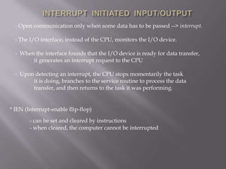
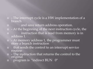
The document discusses interrupt-initiated input/output in computer systems. It explains that when an I/O device is ready to transfer data, it generates an interrupt request to the CPU. The CPU then stops its current task, branches to an interrupt service routine to process the data transfer, before returning to its original task. It provides a flowchart of the interrupt cycle and describes the register transfer operations that occur, including saving the return address and branching to an interrupt handling location in memory. Finally, it outlines the basic hardware components of a computer, including memory, registers, decoders, and control logic gates.