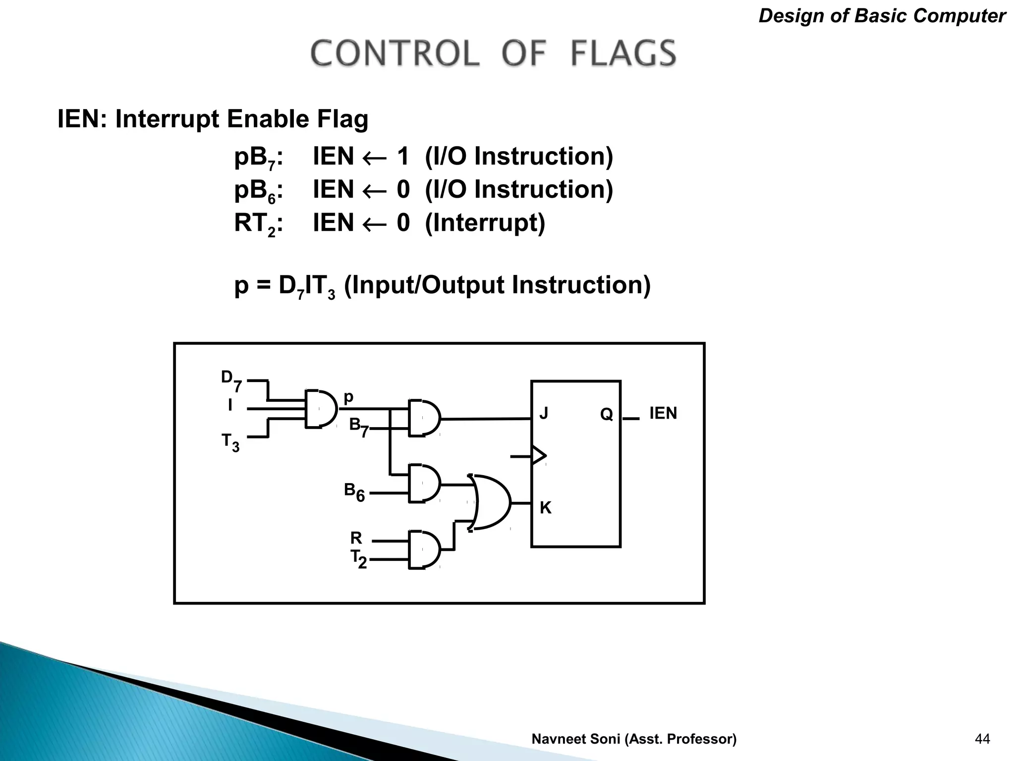
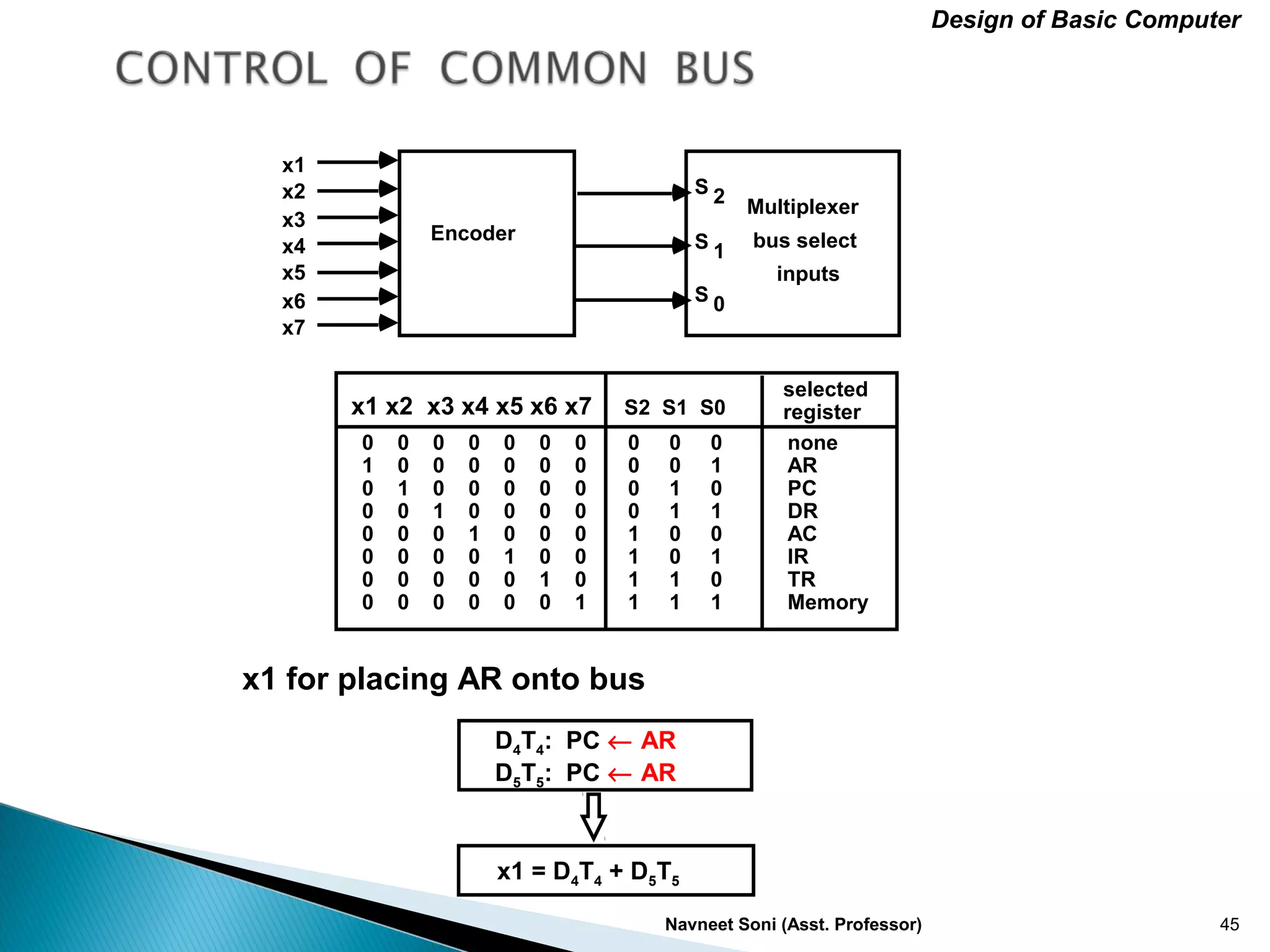
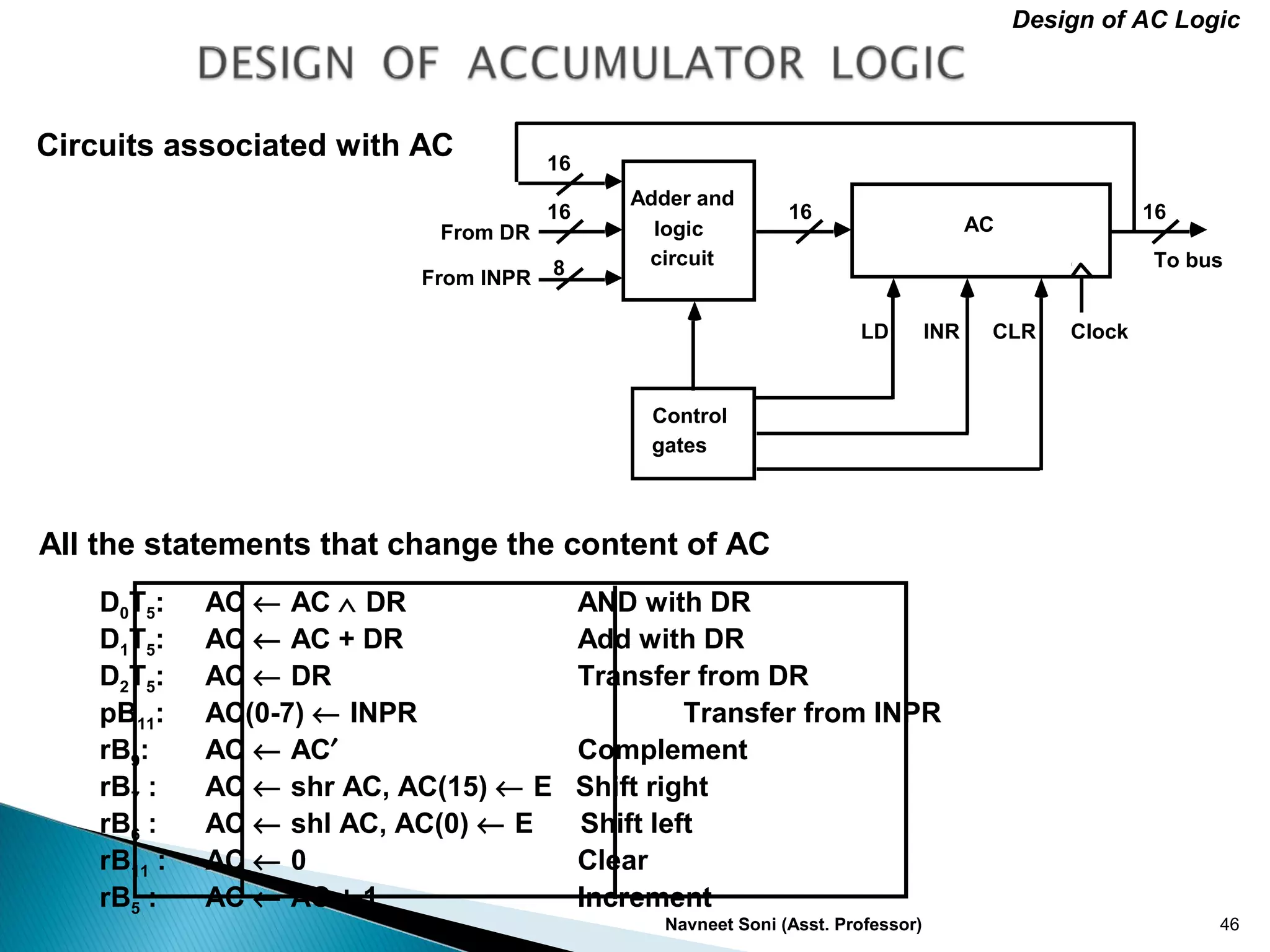
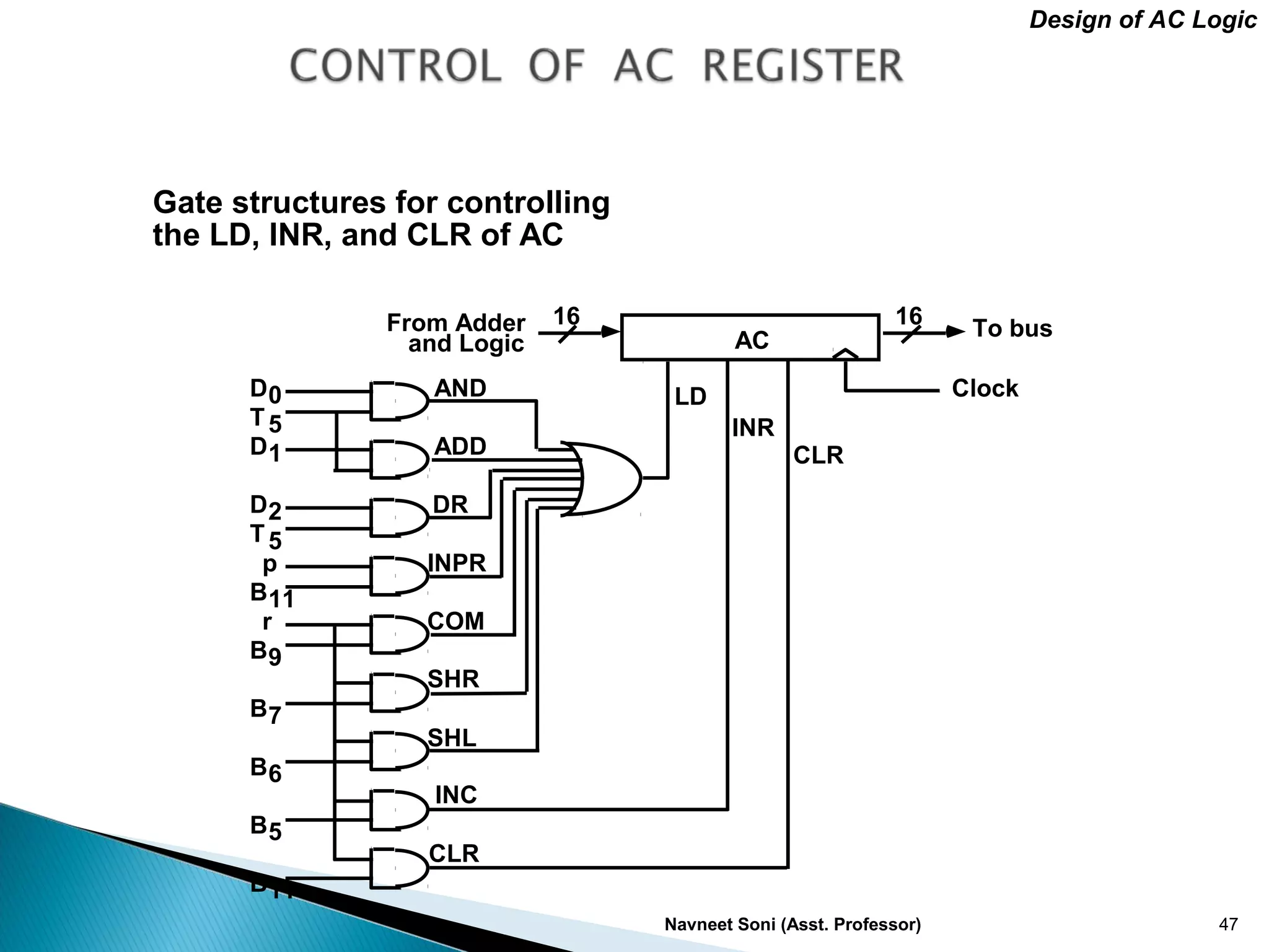
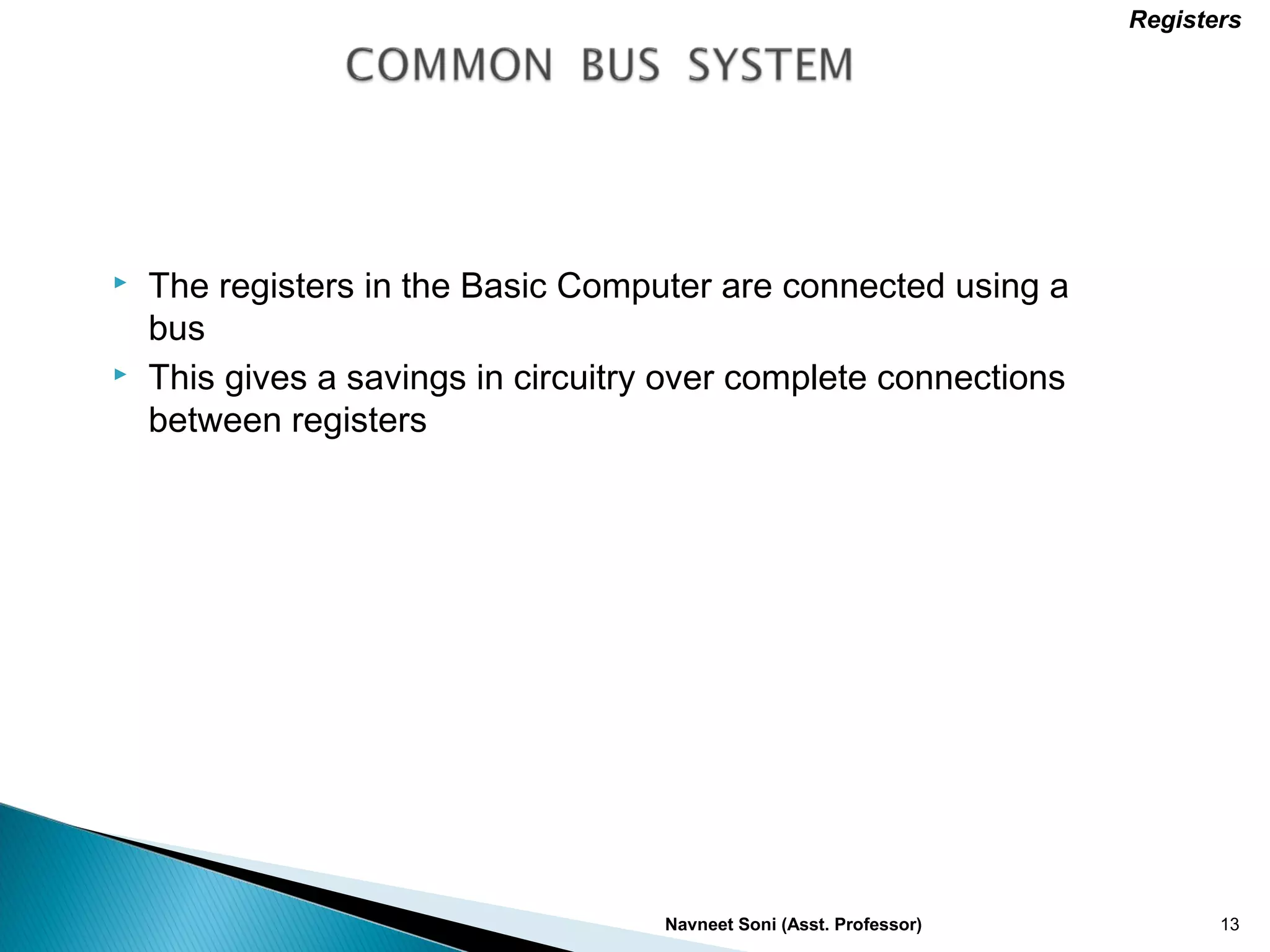
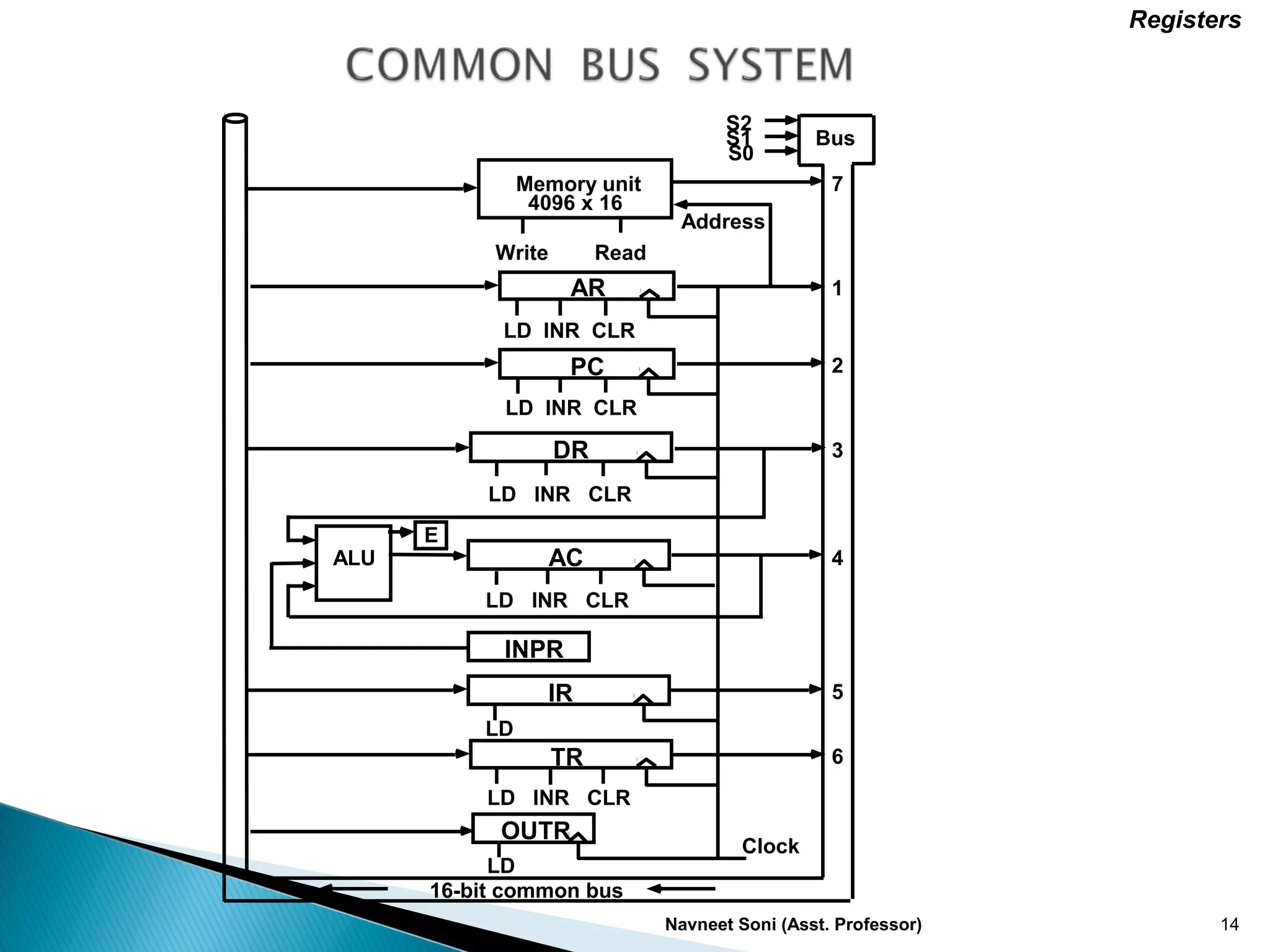
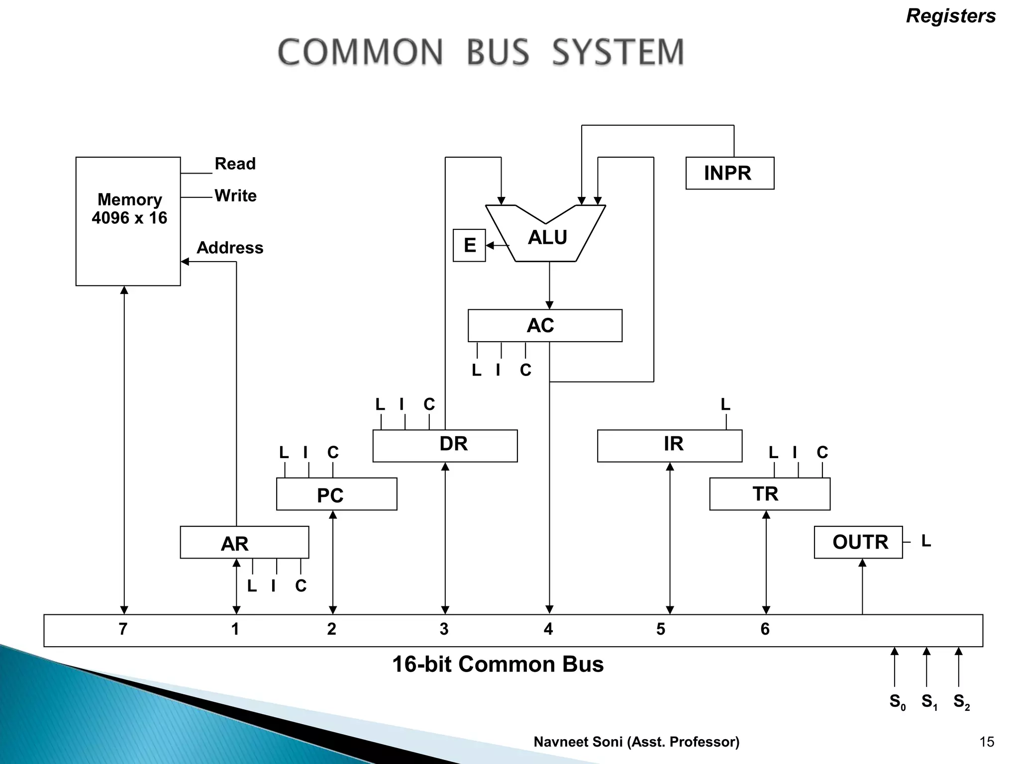
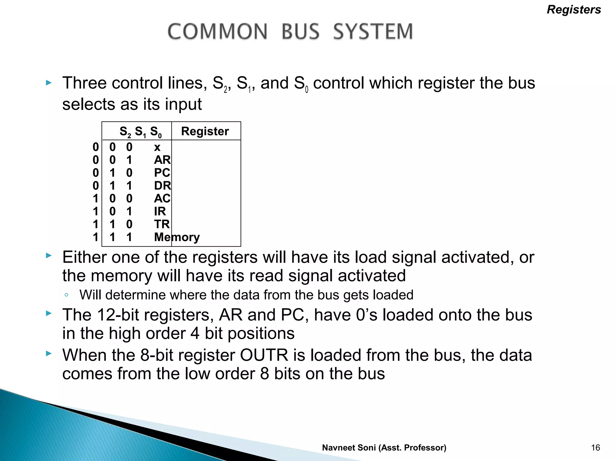
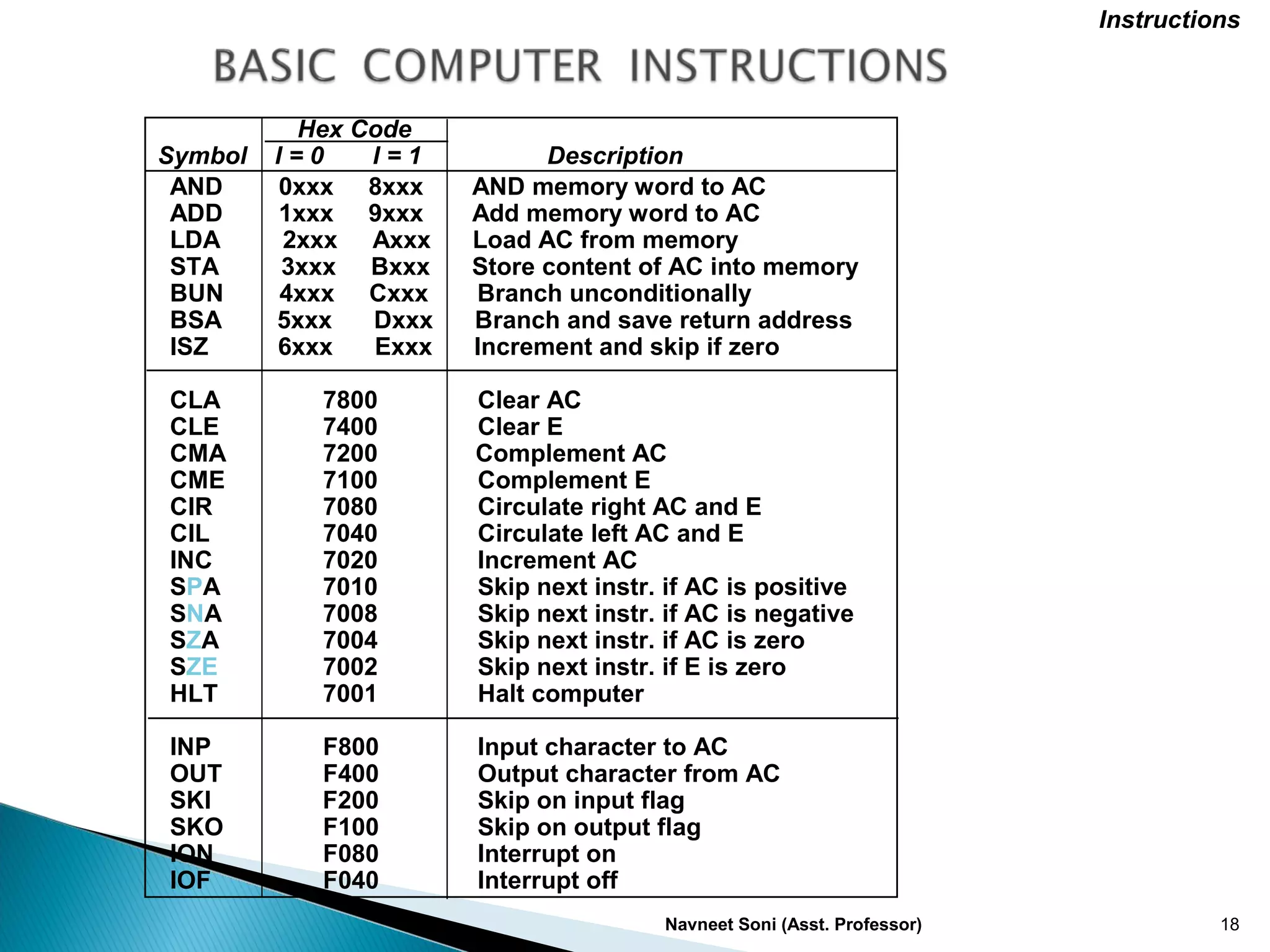
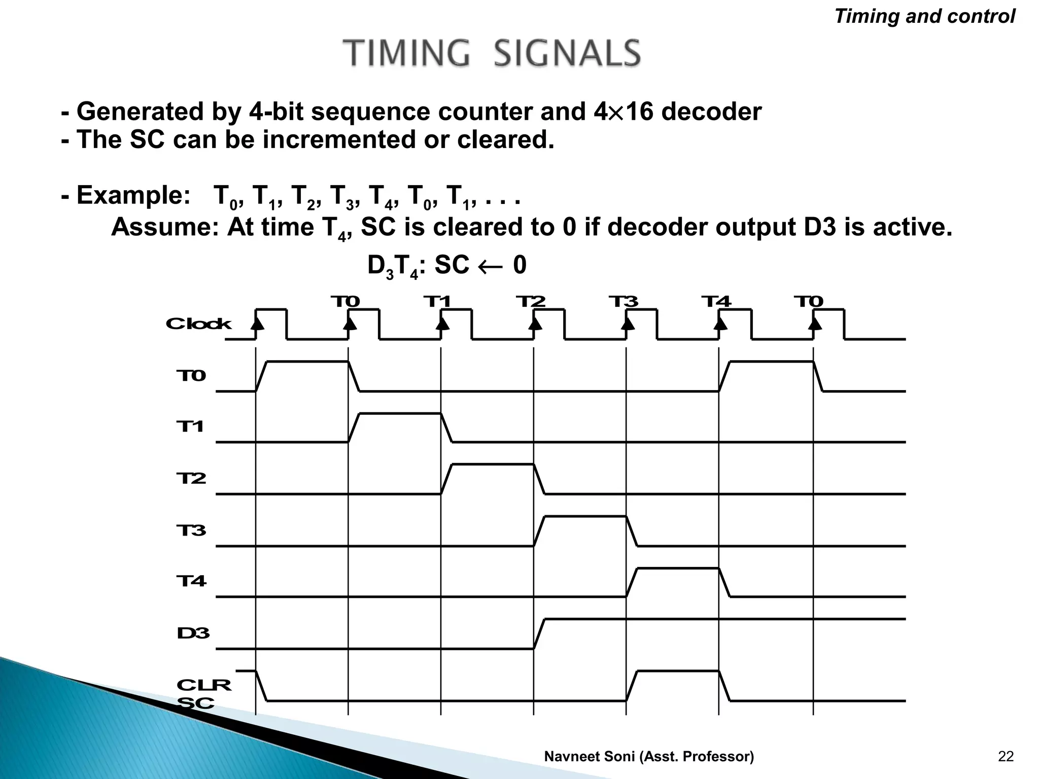
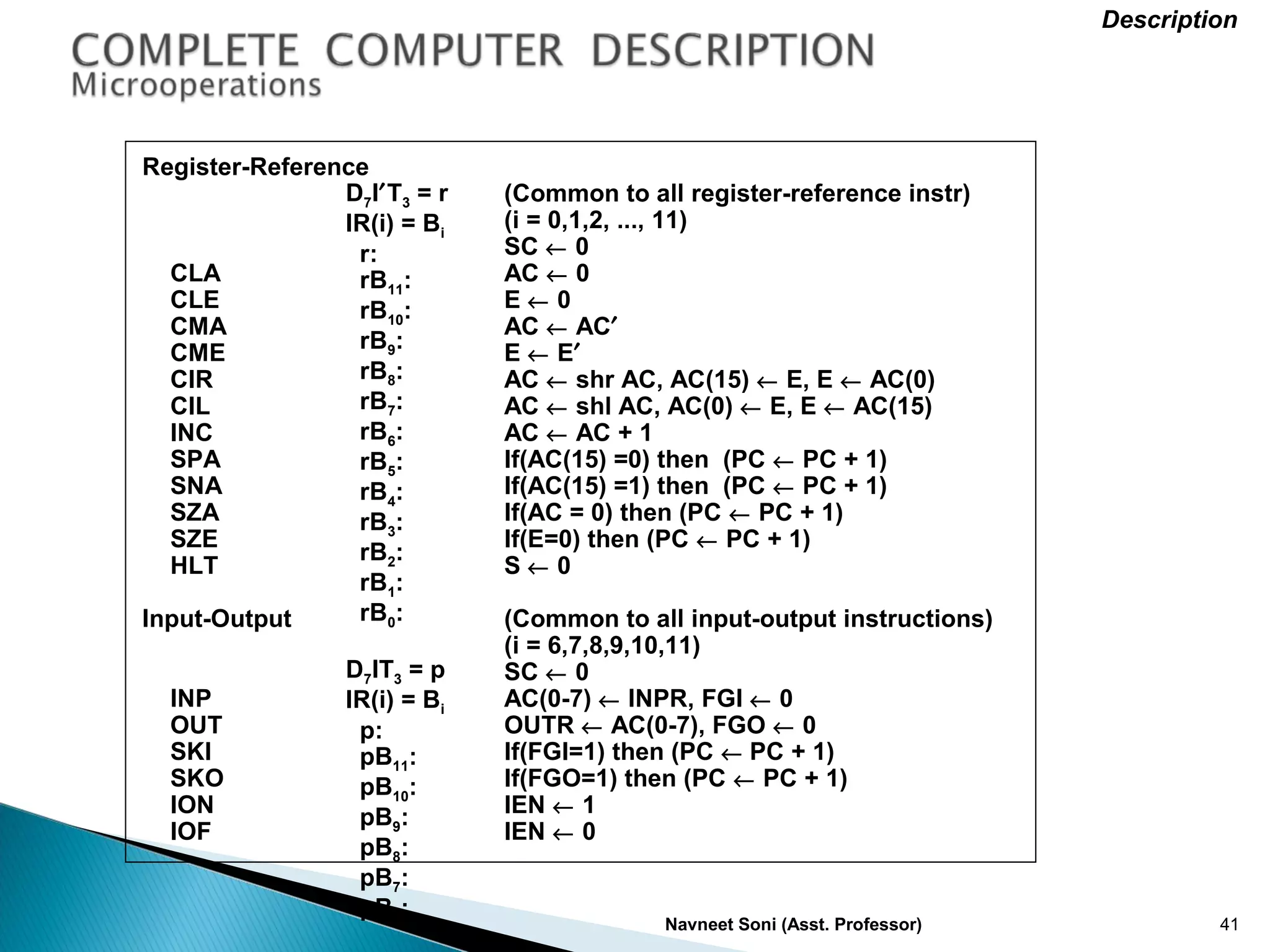
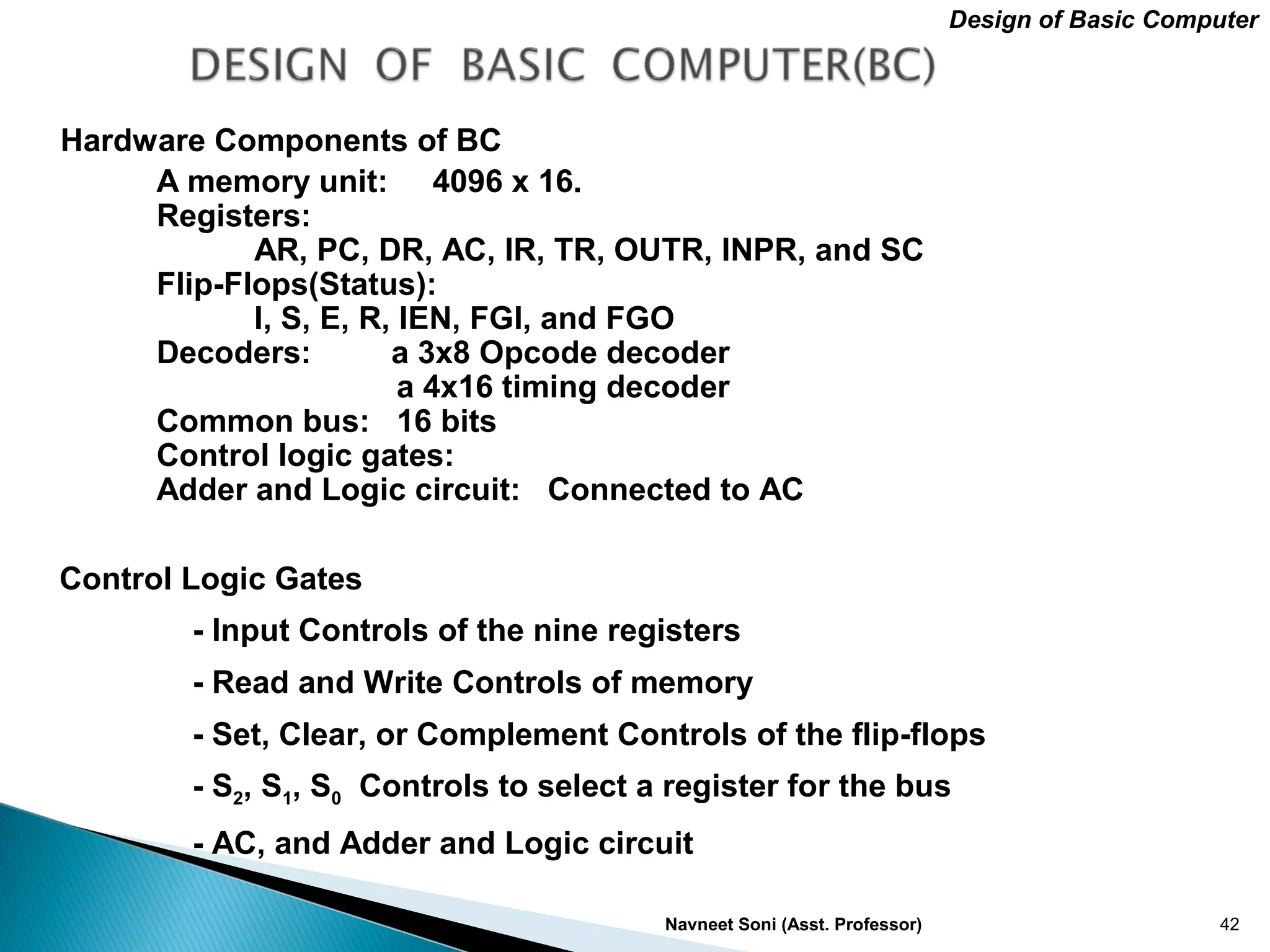
The document discusses the structure and function of a basic computer, detailing components like the processor, memory, instruction formats, and the organization of registers. It explains the roles of various registers, such as the instruction register, program counter, and accumulator, in executing instructions and managing data. Additionally, it covers instruction types, addressing modes, and the control unit's implementation, emphasizing a simplified model of a computer processor.


![Navneet Soni (Asst. Professor) 24
• Fetch and Decode T0: AR ← PC (S0S1S2=010, T0=1)
T1: IR ← M [AR], PC ← PC + 1 (S0S1S2=111, T1=1)
T2: D0, . . . , D7 ← Decode IR(12-14), AR ← IR(0-11), I ← IR(15)
S2
S1
S0
Bus
7
Memory
unit
Address
Read
AR
LD
PC
INR
IR
LD Clock
1
2
5
Common bus
T1
T0
Instruction Cycle](https://image.slidesharecdn.com/csanavneetsoni-160518045540/75/Computer-Organization-and-Architecture-24-2048.jpg)
![Navneet Soni (Asst. Professor) 25
= 0 (direct)
D'7IT3: AR ← M[AR]
D'7I'T3: Nothing
D7I'T3: Execute a register-reference instr.
D7IT3: Execute an input-output instr.
Instrction Cycle
Start
SC ← 0
AR ← PC
T0
IR ← M[AR], PC ← PC + 1
T1
AR ← IR(0-11), I ← IR(15)
Decode Opcode in IR(12-14),
T2
D7
= 0 (Memory-reference) =>opcode ≠ 111(Register or I/O) = 1
II
Execute
register-reference
instruction
SC ← 0
Execute
input-output
instruction
SC ← 0
M[AR]←AR Nothing
= 0 (register)(I/O) = 1 (indirect) = 1
T3 T3 T3 T3
Execute
memory-reference
instruction
SC ← 0
T4](https://image.slidesharecdn.com/csanavneetsoni-160518045540/75/Computer-Organization-and-Architecture-25-2048.jpg)
![Navneet Soni (Asst. Professor) 27
AND to AC
D0T4: DR ← M[AR] Read operand
D0T5: AC ← AC ∧ DR, SC ← 0 AND with AC
ADD to AC
D1T4: DR ← M[AR] Read operand
D1T5: AC ← AC + DR, E ← Cout, SC ← 0 Add to AC and store carry in E
- The effective address of the instruction is in AR and was placed there during
timing signal T2 when I = 0, or during timing signal T3 when I = 1
- Memory cycle is assumed to be short enough to complete in a CPU cycle
- The execution of MR instruction starts with T4
MR Instructions
Symbol
Operation
Decoder
Symbolic Description
AND D0 AC ← AC ∧ M[AR]
ADD D1 AC ← AC + M[AR], E ← Cout
LDA D2 AC ← M[AR]
STA D3 M[AR] ← AC
BUN D4 PC ← AR
BSA D5 M[AR] ← PC, PC ← AR + 1
ISZ D6 M[AR] ← M[AR] + 1, if M[AR] + 1 = 0 then PC ← PC+1](https://image.slidesharecdn.com/csanavneetsoni-160518045540/75/Computer-Organization-and-Architecture-27-2048.jpg)
![Navneet Soni (Asst. Professor) 28
Memory, PC after execution
21
0 BSA 135
Next instruction
Subroutine
20
PC = 21
AR = 135
136
1 BUN 135
Memory, PC, AR at time T4
0 BSA 135
Next instruction
Subroutine
20
21
135
PC = 136
1 BUN 135
Memory Memory
LDA: Load to AC
D2T4: DR ← M[AR]
D2T5: AC ← DR, SC ← 0
STA: Store AC
D3T4: M[AR] ← AC, SC ← 0
BUN: Branch Unconditionally
D4T4: PC ← AR, SC ← 0
BSA: Branch and Save Return Address](https://image.slidesharecdn.com/csanavneetsoni-160518045540/75/Computer-Organization-and-Architecture-28-2048.jpg)
![Navneet Soni (Asst. Professor) 29
MR Instructions
BSA:
D5T4: M[AR] ← PC, AR ← AR + 1
D5T5: PC ← AR, SC ← 0
ISZ: Increment and Skip-if-Zero
D6T4: DR ← M[AR]
D6T5: DR ← DR + 1
D6T4: M[AR] ← DR, if (DR = 0) then (PC ← PC + 1), SC ← 0](https://image.slidesharecdn.com/csanavneetsoni-160518045540/75/Computer-Organization-and-Architecture-29-2048.jpg)
![Navneet Soni (Asst. Professor) 30
MR Instructions
Memory-reference instruction
DR ← M[AR] DR ← M[AR] DR ← M[AR] M[AR] ← AC
SC ← 0
AND ADD LDA STA
AC ← AC DR
SC ← 0
AC ← AC + DR
E ← Cout
SC ← 0
AC ← DR
SC ← 0
D T0 4 D T1 4 D T2 4 D T3 4
D T0 5 D T1 5 D T2 5
PC ← AR
SC ← 0
M[AR] ← PC
AR ← AR + 1
DR ← M[AR]
BUN BSA ISZ
D T4 4 D T5 4 D T6 4
DR ← DR + 1
D T5 5 D T6 5
PC ← AR
SC ← 0
M[AR] ← DR
If (DR = 0)
then (PC ← PC + 1)
SC ← 0
D T6 6
∧](https://image.slidesharecdn.com/csanavneetsoni-160518045540/75/Computer-Organization-and-Architecture-30-2048.jpg)
![Navneet Soni (Asst. Professor) 36
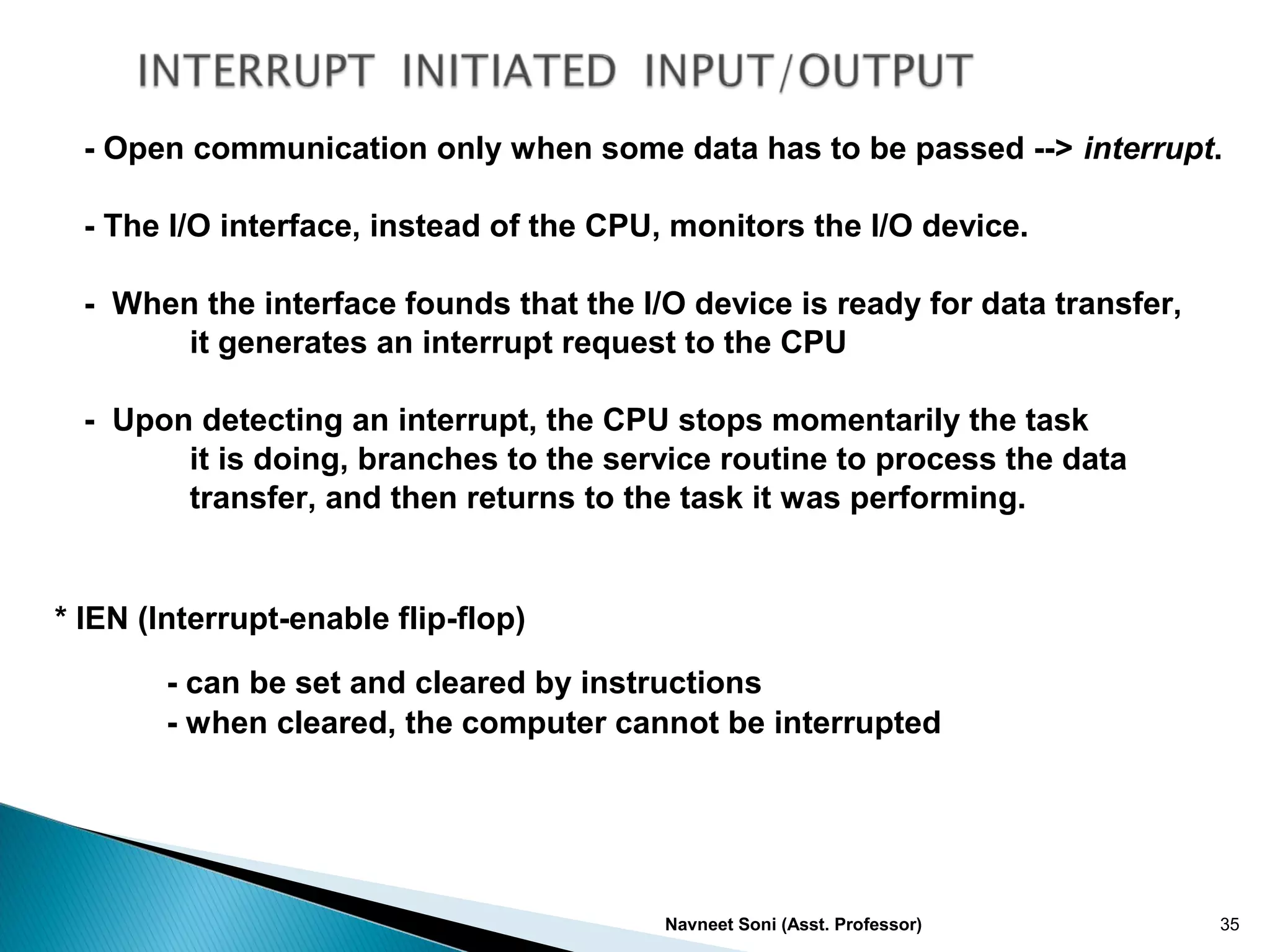
R = Interrupt f/f
- The interrupt cycle is a HW implementation of a branch
and save return address operation.
- At the beginning of the next instruction cycle, the
instruction that is read from memory is in address 1.
- At memory address 1, the programmer must store a branch instruction
that sends the control to an interrupt service routine
- The instruction that returns the control to the original
program is "indirect BUN 0"
I/O and Interrupt
Store return address
R
=1=0
in location 0
M[0] ← PC
Branch to location 1
PC ← 1
IEN ← 0
R ← 0
Interrupt cycleInstruction cycle
Fetch and decode
instructions
IEN
FGI
FGO
Execute
instructions
R ← 1
=1
=1
=1
=0
=0
=0](https://image.slidesharecdn.com/csanavneetsoni-160518045540/75/Computer-Organization-and-Architecture-36-2048.jpg)
![Navneet Soni (Asst. Professor) 37
Register Transfer Statements for Interrupt Cycle
- R F/F ← 1 if IEN (FGI + FGO)T0′T1′T2′
⇔ T0′T1′T2′ (IEN)(FGI + FGO): R ← 1
- The fetch and decode phases of the instruction cycle
must be modified Replace T0, T1, T2 with R'T0, R'T1, R'T2
- The interrupt cycle :
RT0: AR ← 0, TR ← PC
RT1: M[AR] ← TR, PC ← 0
RT2: PC ← PC + 1, IEN ← 0, R ← 0, SC ← 0
After interrupt cycle
0 BUN 1120
0
1
PC = 256
255
1 BUN 0
Before interrupt
Main
Program
1120
I/O
Program
0 BUN 1120
0
PC = 1
256
255
1 BUN 0
Memory
Main
Program
1120
I/O
Program
256
I/O and Interrupt](https://image.slidesharecdn.com/csanavneetsoni-160518045540/75/Computer-Organization-and-Architecture-37-2048.jpg)
![Navneet Soni (Asst. Professor) 39
Description
=1 (I/O) =0 (Register) =1(Indir) =0(Dir)
start
SC ← 0
R
AR ← PC
R’T0
IR ← M[AR], PC ← PC + 1
R’T1
AR ← IR(0~11), I ← IR(15)
D0...D7 ← Decode IR(12 ~ 14)
R’T2
AR ← 0, TR ← PC
RT0
M[AR] ← TR, PC ← 0
RT1
PC ← PC + 1, IEN ← 0
R ← 0, SC ← 0
RT2
D7
I I
Execute
I/O
Instruction
Execute
RR
Instruction
AR <- M[AR] Idle
D7IT3 D7I’T3 D7’IT3 D7’I’T3
Execute MR
Instruction
=0(Instruction =1 (interrupt
Cycle) Cycle)
=1(Register or I/O) =0(Memory Ref)
D7’T4
IEN
FGI
FGO
=1
=1
=1
=0
=0
=0
R ← 1](https://image.slidesharecdn.com/csanavneetsoni-160518045540/75/Computer-Organization-and-Architecture-39-2048.jpg)
![Navneet Soni (Asst. Professor) 40
Description
Fetch
Decode
Indirect
Interrupt
Memory-Reference
AND
ADD
LDA
STA
BUN
BSA
ISZ
R′T0:
R′T1:
R′T2:
D7′IT3:
RT0:
RT1:
RT2:
D0T4:
D0T5:
D1T4:
D1T5:
D2T4:
D2T5:
D3T4:
D4T4:
D5T4:
D5T5:
D6T4:
D6T5:
D6T6:
AR ← PC
IR ← M[AR], PC ← PC + 1
D0, ..., D7 ← Decode IR(12 ~ 14),
AR ← IR(0 ~ 11), I ← IR(15)
AR ← M[AR]
R ← 1
AR ← 0, TR ← PC
M[AR] ← TR, PC ← 0
PC ← PC + 1, IEN ← 0, R ← 0, SC ← 0
DR ← M[AR]
AC ← AC ∧ DR, SC ← 0
DR ← M[AR]
AC ← AC + DR, E ← Cout, SC ← 0
DR ← M[AR]
AC ← DR, SC ← 0
M[AR] ← AC, SC ← 0
PC ← AR, SC ← 0
M[AR] ← PC, AR ← AR + 1
PC ← AR, SC ← 0
DR ← M[AR]
DR ← DR + 1
M[AR] ← DR, if(DR=0) then (PC ← PC + 1),
SC ← 0
T0′T1′T2′(IEN)(FGI + FGO):](https://image.slidesharecdn.com/csanavneetsoni-160518045540/75/Computer-Organization-and-Architecture-40-2048.jpg)
![Navneet Soni (Asst. Professor) 43
Scan all of the register transfer statements that change the content of AR:
LD(AR) = R'T0 + R'T2 + D'7IT3
CLR(AR) = RT0
INR(AR) = D5T4
Address Register; AR
R’T0: AR ← PC LD(AR)
R’T2: AR ← IR(0-11) LD(AR)
D’7IT3: AR ← M[AR] LD(AR)
RT0: AR ← 0 CLR(AR)
D5T4: AR ← AR + 1 INR(AR)
Design of Basic Computer
AR
LD
INR
CLR
Clock
To bus
12
From bus
12
D'
I
T
T
R
T
D
T
7
3
2
0
4](https://image.slidesharecdn.com/csanavneetsoni-160518045540/75/Computer-Organization-and-Architecture-43-2048.jpg)