Downloaded 290 times


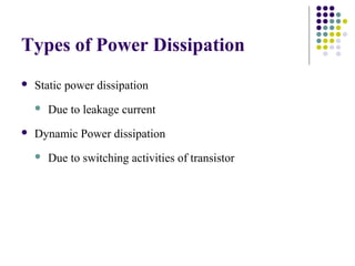
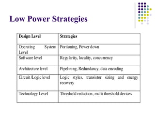
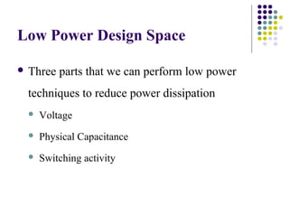


The document discusses low power VLSI design strategies by Vinchip Systems, emphasizing the importance of reducing power dissipation in handheld devices for better performance and battery life. It outlines various techniques including supply voltage reduction, minimizing physical capacitance, and optimizing switching activity. The document also highlights power management strategies and CAD methodologies that can be integrated at different design stages to achieve low power consumption.


