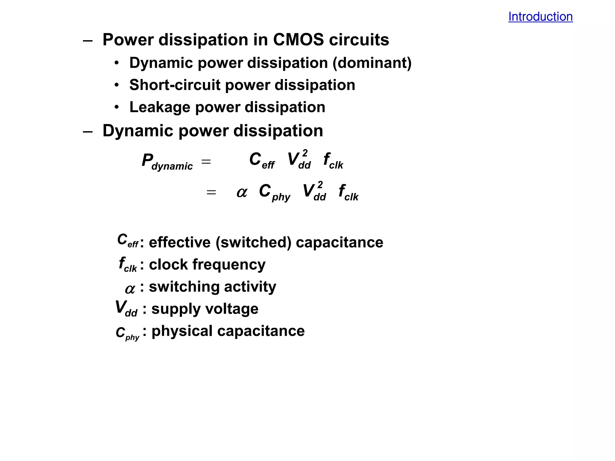
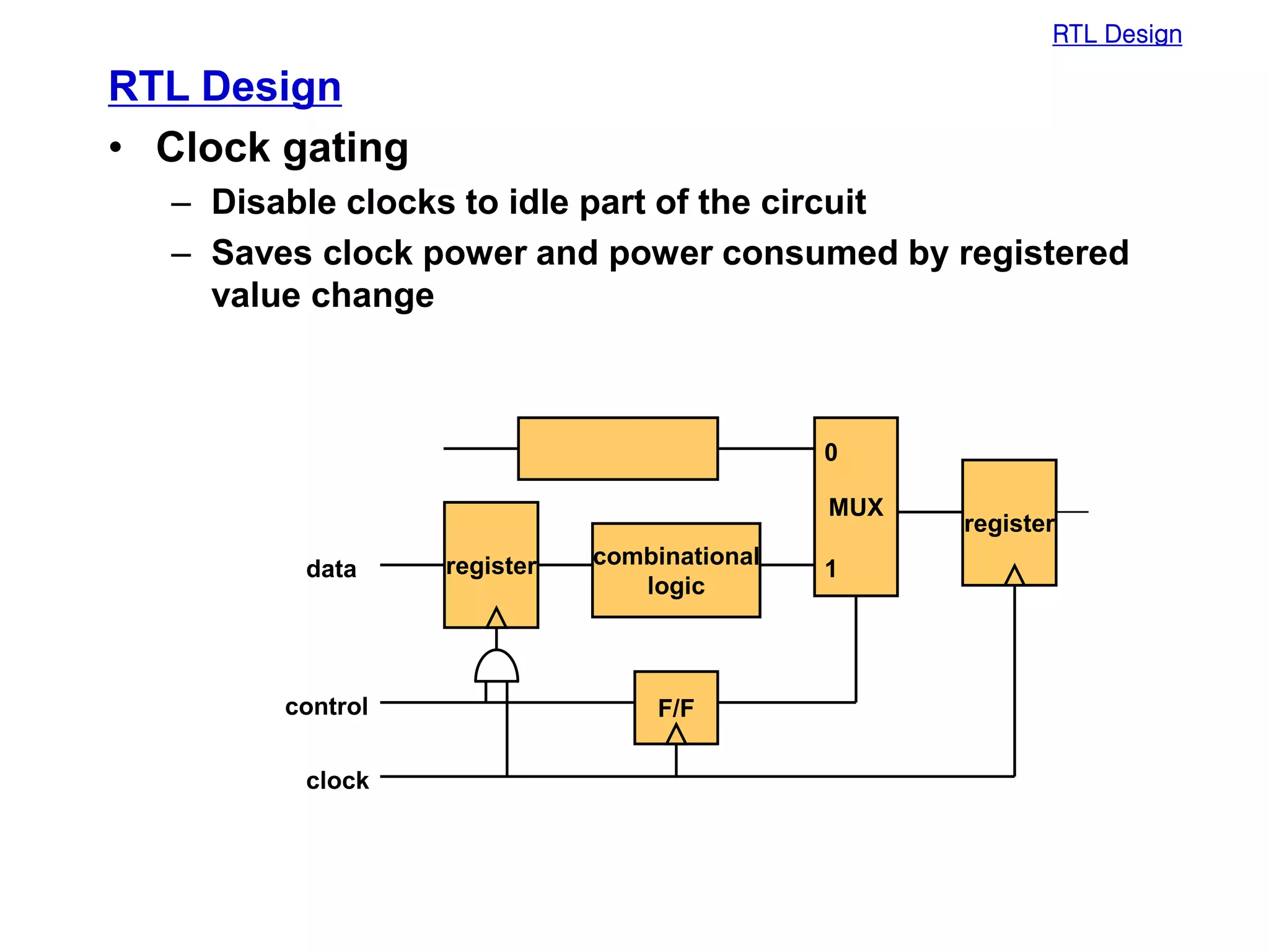
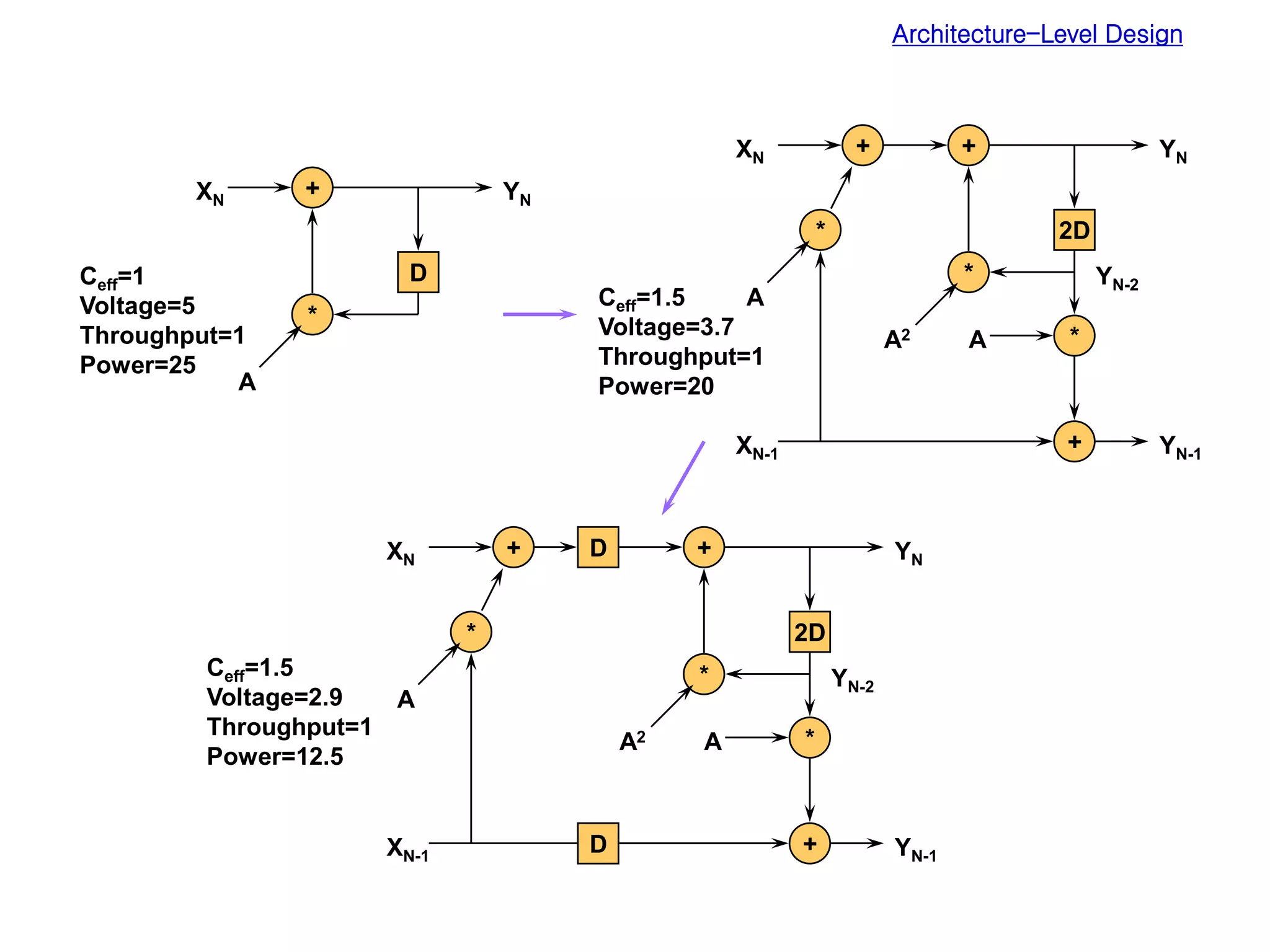
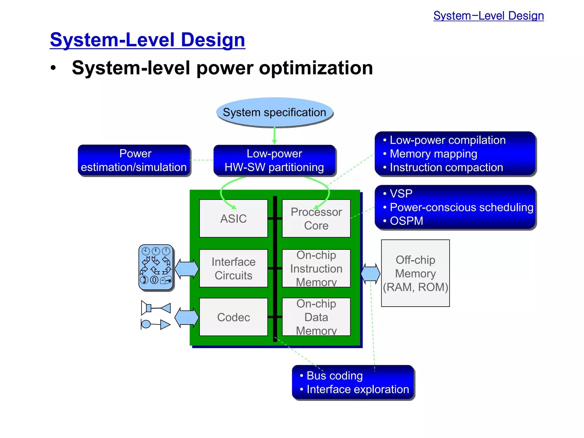
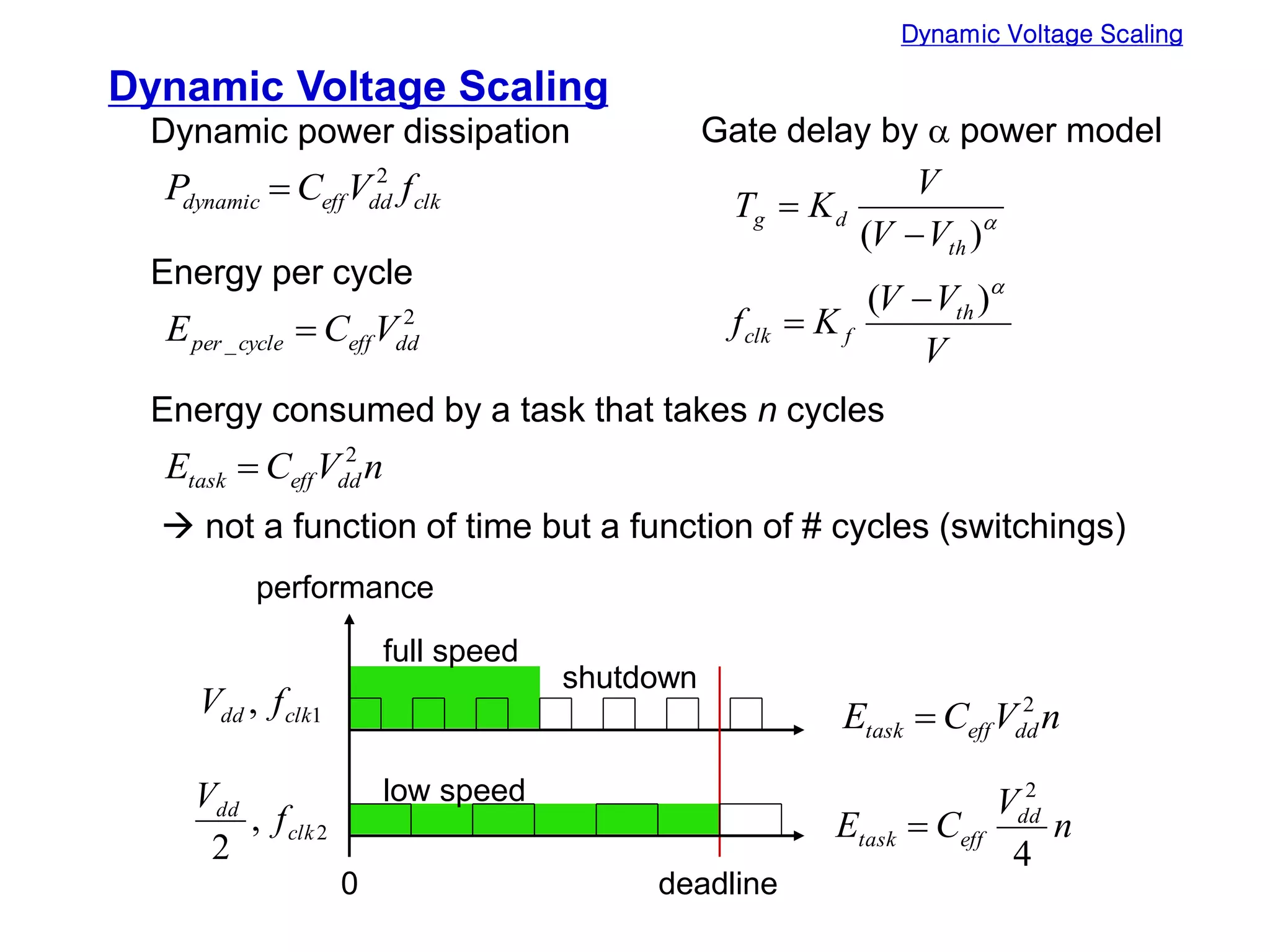
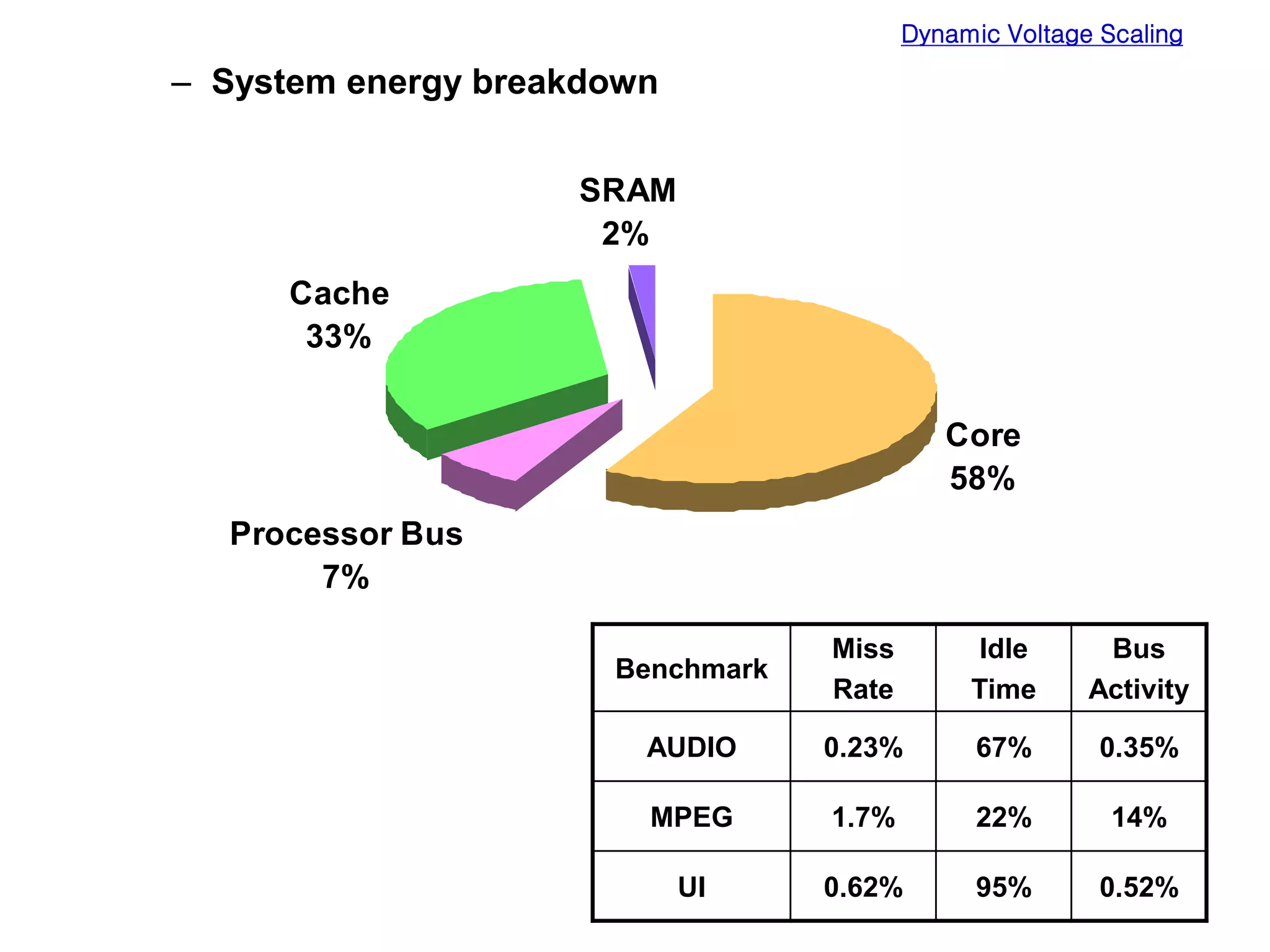
Low power design can be performed at multiple levels of abstraction to significantly reduce power consumption. At the system level, opportunities exist through hardware-software partitioning, dynamic voltage scaling, and bus encoding. At the architecture level, supply voltage reduction, reducing switching activity through operand sharing, and scheduling and binding techniques can lower power. At the RTL level, clock gating, operand isolation, and pre-computation are effective. At lower levels, transistor sizing, interconnect optimization, and de-glitching reduce power. Real-time scheduling on variable speed processors allows exploiting idle times to leverage power-down modes.


![RTL Design
– Comparator example
register
MUX
A>B
register
F/F
0
1
combinational
logic
register
A[MSB]
B[MSB]](https://image.slidesharecdn.com/8891-230102105539-7a59225c/75/8891-ppt-11-2048.jpg)


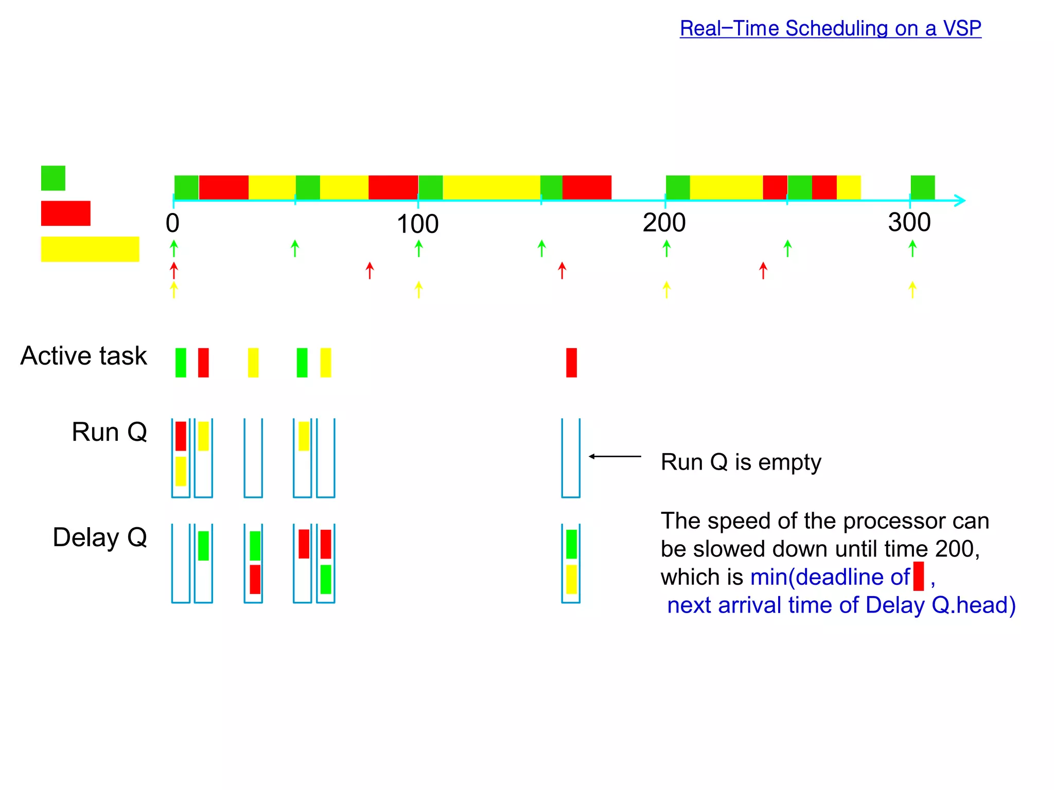
![Real-Time Scheduling on a VSP
0 100 200 300
BCET/WCET
0.0
0.1
0.2
0.3
0.4
0.5
0.6
0.7
0.8
0.9
1.0
3D-image
diesel
fft
bsort
smooth
blue
check-
data
whetstone
line
The chance for speed control increases
as the variation of execution time increases.
Variation of execution time [Ernst 97]](https://image.slidesharecdn.com/8891-230102105539-7a59225c/75/8891-ppt-26-2048.jpg)