International Journal of Computational Engineering Research(IJCER) is an intentional online Journal in English monthly publishing journal. This Journal publish original research work that contributes significantly to further the scientific knowledge in engineering and Technology.
Improved Power Gating Technique for Leakage Power Reductioninventy
Research Inventy : International Journal of Engineering and Science is published by the group of young academic and industrial researchers with 12 Issues per year. It is an online as well as print version open access journal that provides rapid publication (monthly) of articles in all areas of the subject such as: civil, mechanical, chemical, electronic and computer engineering as well as production and information technology. The Journal welcomes the submission of manuscripts that meet the general criteria of significance and scientific excellence. Papers will be published by rapid process within 20 days after acceptance and peer review process takes only 7 days. All articles published in Research Inventy will be peer-reviewed.
Power Gating Based Ground Bounce Noise ReductionIJERA Editor
As low power circuits are most popular the decrease in supply voltage leads to increase in leakage power with respect to the technology scaling. So for removing this kind of leakages and to provide a better power efficiency many power gating techniques are used. But the leakage due to ground connection to the active part of the circuit is very high rather than all other leakages. As it is mainly due to the back EMF of the ground connection it was called it as ground bounce noise. To reduce this noise different methodologies are designed. In this paper the design of such an efficient technique related to ground bounce noise reduction using power gating circuits and comparing the results using DSCH and Microwind low power tools. In this paper the analysis of adders such as full adders using different types of power gated circuits using low power VLSI design techniques and to present the comparison results between different power gating methods.
Design of 64 bit SRAM using Lector Technique for Low Leakage Power with Read ...IOSRJVSP
: In complementary metal oxide semiconductor (CMOS) the power dissipation predominantly comprises of dynamic as well as static power. Prior to introduction of “Deep submicron technologies” it is observed that in case of technology process with feature size larger than 1micro meter, the consumption of dynamic power out of the overall power consumption of any circuit is more than 90%,while that of static power is negligible. But in the present deep submicron technologies in order to, reduce the dynamic power consumption in VLSI circuits, the power supply is being scaled down, keeping in view the principle that the dynamic power dissipated is directly proportional to the square of the supply voltage (Vdd).The threshold voltage also needs to be reduced since the supply voltage is scaled down. Overcoming the inherent limitations in the existing method for leakage power reduction, The Lector (Leakage controlled transistor) technique which works efficiently both in active and idle states of the circuit and results in better leakage power reduction is now proposed. The proposed system presents the analysis of power on “64-bit SRAM array using leakage controlled transistor technique
Power gating is the main power reduction techniques for the static power. As long as technology scaling is taking place, static power becomes paramount important factor to the VLSI designs.Therefore Power gating is the recent power reduction technique that is actively in research areas.
International Journal of Engineering Research and Applications (IJERA) is an open access online peer reviewed international journal that publishes research and review articles in the fields of Computer Science, Neural Networks, Electrical Engineering, Software Engineering, Information Technology, Mechanical Engineering, Chemical Engineering, Plastic Engineering, Food Technology, Textile Engineering, Nano Technology & science, Power Electronics, Electronics & Communication Engineering, Computational mathematics, Image processing, Civil Engineering, Structural Engineering, Environmental Engineering, VLSI Testing & Low Power VLSI Design etc.
Analysis of CMOS and MTCMOS Circuits Using 250 Nano Meter Technology csandit
The low-power consumption with less delay time has become an important issue in the recent
trends of VLSI. In these days, the low power systems with high speed are highly preferable
everywhere. Designers need to understand how low-power techniques affect performance
attributes, and have to choose a set of techniques that are consistent with these attributes .The
main objective of this paper is to describe, how to achieve low power consumption with
approximately same delay time in a single circuit. In this paper, we make circuits with CMOS
and MTCMOS techniques and check out its power and delay characteristics. The circuits
designed using MTCMOS technique gives least power consumption.
All the pre-layout simulations have been performed at 250nm technology on tanner EDA tool.
High performance novel dual stack gating technique for reduction of ground bo...eSAT Journals
Abstract The development of digital integrated circuits is challenged by higher power consumption. The combination of higher clock speeds, greater functional integration, and smaller process geometries has contributed to significant growth in power density. Today leakage power has become an increasingly important issue in processor hardware and software design. So to reduce the leakages in the circuit many low power strategies are identified and experiments are carried out. But the leakage due to ground connection to the active part of the circuit is very higher than all other leakages. As it is mainly due to the back EMF of the ground connection we are calling it as ground bounce noise. To reduce this noise, different methodologies are designed. In this paper, a number of critical considerations in the sleep transistor design and implementation includes header or footer switch selection, sleep transistor distribution choices and sleep transistor gate length, width and body bias optimization for area, leakage and efficiency. Novel dual stack technique is proposed that reduces not only the leakage power but also dynamic power. The previous techniques are summarized and compared with this new approach and comparison of both the techniques is done with the help of Digital Schematic( DSCH ) and Microwind low power tools. Stacking power gating technique has been analyzed and the conditions for the important design parameters (Minimum ground bounce noise) have been derived. The Monte-Carlo simulation is performed in Microwind to calculate the values of all the needed parameters for comparison. Index Terms: Ground Bounce Noise ,Power gating schemes ,Static power dissipation, Dynamic power dissipation, Power gating parameters, Sleep transistors, Novel dual stack approach, Transistor leakage power
The low power has been the main concern for the VLSI industry with the technology scaling in CMOS process from 130 nm to 22nm. The presentation here gives a brief idea about the several low power VLSI techniques being used in VLSI circuits to reduce the power and delay. for any query feel free to visit us at: http://www.siliconmentor.com/
A new improved mcml logic for dpa resistant circuitsVLSICS Design
Security of electronic data remains the major conce
rn. The art of encryption to secure the data can be
achieved in various levels of abstraction. The choi
ce of the logic style in implementing the security
algorithms has greater significance, and it can enh
ance the ability of providing better resistance to
side
channel attacks. The static CMOS logic style is pro
ved to be prone to side channel power attacks. The
exploration of CMOS current mode logic style for re
sistance against these side channel attacks is disc
ussed
in this paper. Various characteristics of the curre
nt mode logic styles, which make it suitable for ma
king
DPA resistant circuits are explored. A new methodol
ogy of biasing the sleep transistors of (MOS curren
t
mode logic) MCML families is proposed. It uses pass
gate transistors for power-gating the circuits. Th
e
power variations of the proposed circuits are compa
red against the standard CMOS counterparts. Logic
gates such as XOR, NAND and AND gate structures of
MCML families and static CMOS are designed and
compared for the ability of side channel resistance
. A distributed arrangement of sleep transistors fo
r
reducing the static power dissipation in the logic
gates is also proposed, designed and analyzed. All
the
logic gates in MCML and CMOS were implemented using
standard 180 nm CMOS technology employing
Cadence® EDA tools.
Sources of Power Dissipation
Dynamic Power Dissipation
Static Power Dissipation
Power Reduction Techniques
Algorithmic Power Minimization
Architectural Power Minimization
Logic and Circuit Level Power Minimization
Control Logic Power Minimization
System Level Power Management.
International Journal of Engineering Research and Applications (IJERA) is an open access online peer reviewed international journal that publishes research and review articles in the fields of Computer Science, Neural Networks, Electrical Engineering, Software Engineering, Information Technology, Mechanical Engineering, Chemical Engineering, Plastic Engineering, Food Technology, Textile Engineering, Nano Technology & science, Power Electronics, Electronics & Communication Engineering, Computational mathematics, Image processing, Civil Engineering, Structural Engineering, Environmental Engineering, VLSI Testing & Low Power VLSI Design etc.
Sub-Threshold Leakage Current Reduction Techniques In VLSI Circuits -A SurveyIJERA Editor
There is an increasing demand for portable devices powered up by battery, this led the manufacturers of
semiconductor technology to scale down the feature size which results in reduction in threshold voltage and
enables the complex functionality on a single chip. By scaling down the feature size the dynamic power
dissipation has no effect but the static power dissipation has become equal or more than that of Dynamic power
dissipation. So in recent CMOS technologies static power dissipation i.e. power dissipation due to leakage
current has become a challenging area for VLSI chip designers. In order to prolong the battery life and maintain
reliability of circuit, leakage current reduction is the primary goal. A basic overview of techniques used for
reduction of sub-threshold leakages is discussed in this paper. Based on the surveyed techniques, one would be
able to choose required and apt leakage reduction technique.
An Efficient Execution of Clock Gating Technique for Logic CircuitsIJTET Journal
Clock gating has been heavily used in reducing the power consumption of the clock network by limiting its activity factor. Fundamentally, clock gating reduces the dynamic power dissipation by disconnecting the clock from an unused circuit block. This result in three major components of power consumption: power consumed by combinational logic whose values are changing on each clock edge; power consumed by flip-flops; power consumed by the clock tree in the design. Here clock gating approach is done for various logic circuits in response to examine its application.
Low Power Electronic design is basically compromised with power aware digital system designs techniques. Especially VLSI power architecture with advanced power reduction techniques are discussed in details here
NOVEL SLEEP TRANSISTOR TECHNIQUES FOR LOW LEAKAGE POWER PERIPHERAL CIRCUITSVLSICS Design
Static power consumption is a major concern in nanometre technologies. Along with technology scaling down and higher operating speeds of CMOS VLSI circuits, the leakage power is getting enhanced. As process geometries are becoming smaller, device density increases and threshold voltage as well as oxide thickness decrease to keep pace with performance. Two novel circuit techniques for leakage current reduction in inverters with and without state retention property are presented in this work. The power dissipation during inactive (standby) mode of operation can be significantly reduced compared to traditional power gating methods by these circuit techniques. The proposed circuit techniques are applied to inverters and the results are compared with earlier inverter leakage minimization techniques. Inverter
buffer chains are designed using new state retention low leakage technique and found to be dissipating lower power with state retention. All low leakage inverters are designed and simulated in cadence design environment using 90 nm technology files. The leakage power during sleep mode is found to be better by X 63 times for novel method. The total power dissipation has also reduced by a factor of X 3.5, compared to earlier sleepy keeper technique. The state retention feature is also good compared to earlier leakage power reduction methodologies.
ANALYSIS OF CMOS AND MTCMOS CIRCUITS USING 250 NANO METER TECHNOLOGYcscpconf
The low-power consumption with less delay time has become an important issue in the recent
trends of VLSI. In these days, the low power systems with high speed are highly preferable
everywhere. Designers need to understand how low-power techniques affect performance
attributes, and have to choose a set of techniques that are consistent with these attributes .The
main objective of this paper is to describe, how to achieve low power consumption with
approximately same delay time in a single circuit. In this paper, we make circuits with CMOS
and MTCMOS techniques and check out its power and delay characteristics. The circuits
designed using MTCMOS technique gives least power consumption.
All the pre-layout simulations have been performed at 250nm technology on tanner EDA tool.
FORCED STACK SLEEP TRANSISTOR (FORTRAN): A NEW LEAKAGE CURRENT REDUCTION APPR...VIT-AP University
Reduction in leakage current has become a significant concern in nanotechnology-based low-power, low-voltage, and high-performance VLSI applications. This research article discusses a new low-power circuit design the approach of FORTRAN (FORced stack sleep TRANsistor), which decreases the leakage power efficiency in the CMOS-based circuit outline in VLSI domain. FORTRAN approach reduces leakage current in both active as well as standby modes of operation. Furthermore, it is not time intensive when the circuit goes from active mode to standby mode and vice-versa. To validate the proposed design approach, experiments are conducted in the Tanner EDA tool of mentor graphics bundle on projected circuit designs for the full adder, a chain of 4-inverters, and 4-bit multiplier designs utilizing 180nm, 130nm, and 90nm TSMC technology node. The outcomes obtained show the result of a 95-98% vital reduction in leakage power as well as a 15-20% reduction in dynamic power with a minor increase in delay. The result outcomes are compared for accuracy with the notable design approaches that are accessible for both active and standby modes of operation.
Low Power Design of Standard Digital Gate Design Using Novel Sleep Transisto...IJMER
In the nanometer range design technologies static power consumption is very important
issue in present peripheral devices. In the CMOS based VLSI circuits technology is scaling towards
down in respect of size and achieving higher operating speeds. We have also considered these
parameters such that we can control the leakage power. As process model design are getting smaller
the density of device increases and threshold voltage as well as oxide thickness decrease to maintain
the device performance. In this article two novel circuit techniques for reduction leakage current in
NAND and NOR inverters using novel sleepy and sleepy property are investigated. We have proposed a
design model that has significant reduction in power dissipation during inactive (standby) mode of
operation compared to classical power gating methods for these circuit techniques. The proposed
circuit techniques are applied to NAND and NOR inverters and the results are compared with earlier
inverter leakage minimization techniques. All low leakage models of inverters are designed and
simulated in Tanner Tool environment using 65 nm CMOS Technology (1volt) technologies. Average
power, Leakage power, sleep transistor
Optimized Design of an Alu Block Using Power Gating TechniqueIJERA Editor
Power is the limiting factor in traditional CMOS scaling and must be dealt with aggressively. With the scaling
of technology and the need for high performance and more functionality, power dissipation becomes a major
bottleneck for a system design. Power gating of functional units has been proved to be an effective technique to
reduce power consumption. This paper describe about to design of an ALU block with sleep mode to reduce the
power consumption of the circuit. Local sleep transistors are used to achieve sleep mode. During sleep mode
one functional unit is working and another functional unit is in idle state. i.e., it disconnects the idle logic
blocks from the power supply. Architecture and functionality of the ALU implemented on FPGA and is tested
using DSCH tool. Power analysis is carried out using MICROWIND tool.
International Journal of Engineering Research and Applications (IJERA) is an open access online peer reviewed international journal that publishes research and review articles in the fields of Computer Science, Neural Networks, Electrical Engineering, Software Engineering, Information Technology, Mechanical Engineering, Chemical Engineering, Plastic Engineering, Food Technology, Textile Engineering, Nano Technology & science, Power Electronics, Electronics & Communication Engineering, Computational mathematics, Image processing, Civil Engineering, Structural Engineering, Environmental Engineering, VLSI Testing & Low Power VLSI Design etc.
A Sub Threshold Source Coupled Logic Based Design of Low Power CMOS Analog Mu...VLSICS Design
A novel approach for designing Ultra Low Power and wide dynamic range circuit for multiplexing analog
signals is presented. The design operates in weak inversion (Sub threshold) region and uses Source -
Coupled Logic ( SCL) circuit. The bias current of the SCL gates is varied to scale down linearly the power
consumption and the operating frequency. The multiplexer design employs CMOS transistors as
transmission gate with dynamic threshold voltage. The design exhibits low power dissipation, high
dynamic range and good linearity. The design was implemented in 180 nm technology and was operated at
a supply voltage of 400 mV with a bias current ranging in the order of few Pico-amperes. The ON and
OFF resistance of the transmission gate achieved were 27 ohms and 10 M ohms respectively. The power
dissipation achieved is around 0.79 μW for a dynamic range of 1μV to 0.4 V.
Design of complex arithmetic logic circuits considering ground noise, leakage current, active power and area is a challenging task in VLSI circuits. In this paper, a comparative analysis of high performance power gating schemes is done which minimizes the leakage power and provides a way to control the ground noise. The innovative power gating schemes such as stacking power gating , diode based stacking power gating are analyzed which minimizes the peak of ground noise in transition mode for deep submicron circuits. Further to evaluate the efficiency, the simulation has been done using such high performance power gating schemes. Leakage current comparison of NAND gate without power gating and with power gating scheme is done. Finally it is observed that the leakage current in standby mode is reduced by 80% over the conventional power gating. It is also found that in stacking power gating, the ground noise has been reduced by a small extent over the conventional power gating scheme. We have performed simulations using Tanner in a 180nm standard CMOS technology at room temperature with supply voltage of 2.5 V. Finally, a detailed comparative analysis has been carried out to measure the design efficiency of high performance power gating schemes. This analysis provides an effective road map for high performance digital circuit designers who are interested to work with low power application in deep submicron circuits.
Design of ultra low power 8 channel analog multiplexer using dynamic threshol...VLSICS Design
The design of an ultra low voltage, low power high
speed 8 channel Analog multiplexer in 180nm CMOS
technology is presented. A modified transmission ga
te using a dynamic threshold voltage MOSFET
(DTMOS
)
is employed in the design. The design is optimized
with respect to critical requirements like short
switching time, low power dissipation, good lineari
ty and high dynamic range with an operating voltage
of
0.4V. The ON and OFF resistances achieved are 32 oh
ms and 10Mohms respectively with a switching
speed of 10MHz. The power dissipation obtained is a
round 2.65uW for a dynamic range of 1uV to 0.4V.
A NOVEL LOW POWER HIGH DYNAMIC THRESHOLD SWING LIMITED REPEATER INSERTION FOR...VLSICS Design
In Very Large Scale Integration (VLSI), interconnect design has become a supreme issue in high speed ICs. With the decreased feature size of CMOS circuits, on-chip interconnect now dominates both circuit delay and power consumption. An eminent technique known as repeater/buffer insertion is used in long interconnections to reduce delay in VLSI circuits. This paper deals with some distinct low power alternative circuits in buffer insertion technique and it proposes two new techniques: Dynamic Threshold Swing Limited (DTSL) and High Dynamic Threshold Swing Limited (HDTSL). The DTSL uses Dynamic Threshold MOSFET configuration. In this gate is tied to the body and it limits the output swing. High Dynamic Threshold Swing Limited (HDTSL) also uses the same configuration along with a high threshold voltage(high-Vth). The simulation results are performed in Cadence virtuoso environment tool using 45nm technology. By simulating and comparing these various repeater circuits along with the proposed circuits it is analyzed that there is trade off among power, delay and Power Delay Product and the 34.66% of power is reduced by using the high- Vth in HDTSL when compared to DTSL.
A novel low power high dynamic threshold swing limited repeater insertion for...VLSICS Design
In Very Large Scale Integration (VLSI), interconnect design has become a supreme issue in high speed ICs.
With the decreased feature size of CMOS circuits, on-chip interconnect now dominates both circuit delay
and power consumption. An eminent technique known as repeater/buffer insertion is used in long
interconnections to reduce delay in VLSI circuits. This paper deals with some distinct low power
alternative circuits in buffer insertion technique and it proposes two new techniques: Dynamic Threshold
Swing Limited (DTSL) and High Dynamic Threshold Swing Limited (HDTSL). The DTSL uses Dynamic
Threshold MOSFET configuration. In this gate is tied to the body and it limits the output swing. High
Dynamic Threshold Swing Limited (HDTSL) also uses the same configuration along with a high threshold
voltage(high-Vth). The simulation results are performed in Cadence virtuoso environment tool using 45nm
technology. By simulating and comparing these various repeater circuits along with the proposed circuits it
is analyzed that there is trade off among power, delay and Power Delay Product and the 34.66% of power
is reduced by using the high- Vth in HDTSL when compared to DTSL.
Extremely Low Power FIR Filter for a Smart Dust Sensor ModuleCSCJournals
Digital filters are common components in many applications today, also in for sensor systems, such as large-scale distributed smart dust sensors. For these applications the power consumption is very critical, it has to be extremely low. With the transistor technology scaling becoming more and more sensitive to e.g. gate leakage, it has become a necessity to find ways to minimize the flow of leakage in current CMOS logic. This paper studies sub-threshold source coupled logic (STSCL) in a 45-nm process. The STSCL can be used instead of traditional CMOS to meet the low power and energy consumption requirements. The STSCL style is in this paper used to design a digital filter, applicable for the audio interface of a smart dust sensor where the sample frequency will be 44.1 kHz. A finite-length impulse response (FIR) filter is used with transposed direct form structure and for the coefficient multiplication five-bit canonic signed digit [7] based serial/parallel multipliers were used. The power consumption is calculated along with the delay in order to present the power delay product (PDP) such that the performance of the sub-threshold logic can be compared with corresponding CMOS implementation. The simulated results shows a significant reduction in energy consumption (in terms of PDP) with the system running at a supply voltage as low as 0.2 V using STSCL.
Back track input vector algorithm for leakage reduction in cmos vlsi digital ...VLSICS Design
A new algorithm based on Input Vector Control (IVC) technique is proposed, which shifts logic gate of a
circuit to its minimum leakage state, when device goes into its idle state. Leakage current in CMOS VLSI
circuit has become a major constrain in a battery operated device for technology node below 90nm, as it
drains the battery even when a circuit is in standby mode. Major concern is the leakage even in run time
condition, here aim is to focus on run time leakage reduction technique of integrated Circuit. It is inherited
by stacking effect when the series transistors are maximized in OFF state condition. This method is
independent of process technology and does not require any additional power supply. This paper gives an
optimized solution of input pattern determination of some small circuit to find minimum leakage vector
considering promising and non-promising node which helps to reduce the time complexity of the algorithm.
Proposed algorithm is simulated using HSPICE simulator for 2 input NAND gate and different standard
logic cells and achieved 94.2% and 54.59 % average leakage power reduction for 2 input NAND cell and
different logics respectively.
Design of Memory Cell for Low Power ApplicationsIJERA Editor
Aggressive CMOS scaling results in lower threshold voltage and thin oxide thickness for transistors manufactured in nano regime. As a result, reducing the sub-threshold and tunneling gate leakage currents has become crucial in the design of ICs. This paper presents a new method to reduce the total leakage power dissipation of static random access memories (SRAMs) while maintaining their performance.
Static power optimization using dual sub threshold supply voltages in digital...VLSICS Design
Power dissipation in high performance systems requi
res more expensive packaging. In this situation, lo
w
power VLSI design has assumed great importance as a
n active and rapidly developing field. As the densi
ty
and operating speed of CMOS VLSI chip increases, st
atic power dissipation becomes more significant. Th
is
is due to the leakage current when the transistor i
s off this is threshold voltage dependent. This can
be
observed in the combinational and sequential circui
ts. Static power reduction techniques are achieved
by
means of operating the transistor either in Cut-off
or in Saturation region completely and avoiding th
e
clock in unnecessary circuits. In this work, “Dual
sub-threshold voltage supply” technique is used to
operate the transistor under off state or either in
on state by applying some voltage at the gate of t
he MOS
transistor. This static power reduction technique i
s to digital circuits, so that the power dissipatio
n is
reduced and the performance of the circuit is incre
ased. The designed circuits can be simulated by usi
ng
Mentor Graphics Backend Tool
International Journal of Engineering Research and Applications (IJERA) is an open access online peer reviewed international journal that publishes research and review articles in the fields of Computer Science, Neural Networks, Electrical Engineering, Software Engineering, Information Technology, Mechanical Engineering, Chemical Engineering, Plastic Engineering, Food Technology, Textile Engineering, Nano Technology & science, Power Electronics, Electronics & Communication Engineering, Computational mathematics, Image processing, Civil Engineering, Structural Engineering, Environmental Engineering, VLSI Testing & Low Power VLSI Design etc.
Similar to International Journal of Computational Engineering Research (IJCER) (20)
DevOps and Testing slides at DASA ConnectKari Kakkonen
My and Rik Marselis slides at 30.5.2024 DASA Connect conference. We discuss about what is testing, then what is agile testing and finally what is Testing in DevOps. Finally we had lovely workshop with the participants trying to find out different ways to think about quality and testing in different parts of the DevOps infinity loop.
Smart TV Buyer Insights Survey 2024 by 91mobiles.pdf91mobiles
91mobiles recently conducted a Smart TV Buyer Insights Survey in which we asked over 3,000 respondents about the TV they own, aspects they look at on a new TV, and their TV buying preferences.
GDG Cloud Southlake #33: Boule & Rebala: Effective AppSec in SDLC using Deplo...James Anderson
Effective Application Security in Software Delivery lifecycle using Deployment Firewall and DBOM
The modern software delivery process (or the CI/CD process) includes many tools, distributed teams, open-source code, and cloud platforms. Constant focus on speed to release software to market, along with the traditional slow and manual security checks has caused gaps in continuous security as an important piece in the software supply chain. Today organizations feel more susceptible to external and internal cyber threats due to the vast attack surface in their applications supply chain and the lack of end-to-end governance and risk management.
The software team must secure its software delivery process to avoid vulnerability and security breaches. This needs to be achieved with existing tool chains and without extensive rework of the delivery processes. This talk will present strategies and techniques for providing visibility into the true risk of the existing vulnerabilities, preventing the introduction of security issues in the software, resolving vulnerabilities in production environments quickly, and capturing the deployment bill of materials (DBOM).
Speakers:
Bob Boule
Robert Boule is a technology enthusiast with PASSION for technology and making things work along with a knack for helping others understand how things work. He comes with around 20 years of solution engineering experience in application security, software continuous delivery, and SaaS platforms. He is known for his dynamic presentations in CI/CD and application security integrated in software delivery lifecycle.
Gopinath Rebala
Gopinath Rebala is the CTO of OpsMx, where he has overall responsibility for the machine learning and data processing architectures for Secure Software Delivery. Gopi also has a strong connection with our customers, leading design and architecture for strategic implementations. Gopi is a frequent speaker and well-known leader in continuous delivery and integrating security into software delivery.
JMeter webinar - integration with InfluxDB and GrafanaRTTS
Watch this recorded webinar about real-time monitoring of application performance. See how to integrate Apache JMeter, the open-source leader in performance testing, with InfluxDB, the open-source time-series database, and Grafana, the open-source analytics and visualization application.
In this webinar, we will review the benefits of leveraging InfluxDB and Grafana when executing load tests and demonstrate how these tools are used to visualize performance metrics.
Length: 30 minutes
Session Overview
-------------------------------------------
During this webinar, we will cover the following topics while demonstrating the integrations of JMeter, InfluxDB and Grafana:
- What out-of-the-box solutions are available for real-time monitoring JMeter tests?
- What are the benefits of integrating InfluxDB and Grafana into the load testing stack?
- Which features are provided by Grafana?
- Demonstration of InfluxDB and Grafana using a practice web application
To view the webinar recording, go to:
https://www.rttsweb.com/jmeter-integration-webinar
PHP Frameworks: I want to break free (IPC Berlin 2024)Ralf Eggert
In this presentation, we examine the challenges and limitations of relying too heavily on PHP frameworks in web development. We discuss the history of PHP and its frameworks to understand how this dependence has evolved. The focus will be on providing concrete tips and strategies to reduce reliance on these frameworks, based on real-world examples and practical considerations. The goal is to equip developers with the skills and knowledge to create more flexible and future-proof web applications. We'll explore the importance of maintaining autonomy in a rapidly changing tech landscape and how to make informed decisions in PHP development.
This talk is aimed at encouraging a more independent approach to using PHP frameworks, moving towards a more flexible and future-proof approach to PHP development.
Neuro-symbolic is not enough, we need neuro-*semantic*Frank van Harmelen
Neuro-symbolic (NeSy) AI is on the rise. However, simply machine learning on just any symbolic structure is not sufficient to really harvest the gains of NeSy. These will only be gained when the symbolic structures have an actual semantics. I give an operational definition of semantics as “predictable inference”.
All of this illustrated with link prediction over knowledge graphs, but the argument is general.
Accelerate your Kubernetes clusters with Varnish CachingThijs Feryn
A presentation about the usage and availability of Varnish on Kubernetes. This talk explores the capabilities of Varnish caching and shows how to use the Varnish Helm chart to deploy it to Kubernetes.
This presentation was delivered at K8SUG Singapore. See https://feryn.eu/presentations/accelerate-your-kubernetes-clusters-with-varnish-caching-k8sug-singapore-28-2024 for more details.
Epistemic Interaction - tuning interfaces to provide information for AI supportAlan Dix
Paper presented at SYNERGY workshop at AVI 2024, Genoa, Italy. 3rd June 2024
https://alandix.com/academic/papers/synergy2024-epistemic/
As machine learning integrates deeper into human-computer interactions, the concept of epistemic interaction emerges, aiming to refine these interactions to enhance system adaptability. This approach encourages minor, intentional adjustments in user behaviour to enrich the data available for system learning. This paper introduces epistemic interaction within the context of human-system communication, illustrating how deliberate interaction design can improve system understanding and adaptation. Through concrete examples, we demonstrate the potential of epistemic interaction to significantly advance human-computer interaction by leveraging intuitive human communication strategies to inform system design and functionality, offering a novel pathway for enriching user-system engagements.
Essentials of Automations: Optimizing FME Workflows with ParametersSafe Software
Are you looking to streamline your workflows and boost your projects’ efficiency? Do you find yourself searching for ways to add flexibility and control over your FME workflows? If so, you’re in the right place.
Join us for an insightful dive into the world of FME parameters, a critical element in optimizing workflow efficiency. This webinar marks the beginning of our three-part “Essentials of Automation” series. This first webinar is designed to equip you with the knowledge and skills to utilize parameters effectively: enhancing the flexibility, maintainability, and user control of your FME projects.
Here’s what you’ll gain:
- Essentials of FME Parameters: Understand the pivotal role of parameters, including Reader/Writer, Transformer, User, and FME Flow categories. Discover how they are the key to unlocking automation and optimization within your workflows.
- Practical Applications in FME Form: Delve into key user parameter types including choice, connections, and file URLs. Allow users to control how a workflow runs, making your workflows more reusable. Learn to import values and deliver the best user experience for your workflows while enhancing accuracy.
- Optimization Strategies in FME Flow: Explore the creation and strategic deployment of parameters in FME Flow, including the use of deployment and geometry parameters, to maximize workflow efficiency.
- Pro Tips for Success: Gain insights on parameterizing connections and leveraging new features like Conditional Visibility for clarity and simplicity.
We’ll wrap up with a glimpse into future webinars, followed by a Q&A session to address your specific questions surrounding this topic.
Don’t miss this opportunity to elevate your FME expertise and drive your projects to new heights of efficiency.
International Journal of Computational Engineering Research (IJCER)
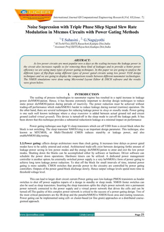
1. International Journal Of Computational Engineering Research||Vol, 03||Issue, 7||
www.ijceronline.com ||July||2013|| Page 29
Noise Supression with Triple Phase Sllep Signal Slew Rate
Modulation in Mtcmos Circuits with Power Gating Methods
1,
T.Suhasini , 2,
G.Nagajyothi
1,
M.Tech(Vlsi),SSITS,Rayachoti,Kadapa Dist,India
2,
Assistant Prof,SSITS,Rayachoti,Kadapa Dist,India
I. INTRODUCTION
The scaling of process technologies to nanometer regime has resulted in a rapid increase in leakage
power disNMOS1pation. Hence, it has become extremely important to develop design techniques to reduce
static power disNMOS1pation during periods of inactivity. The power reduction must be achieved without
trading-off performance which makeNMOS1t harder to reduce leakage during normal (runtime) operation. On
the other hand, there are several techniques for reducing leakage power in sleep or standby mode. Power gating
is one such well known technique where a sleep transistor is added between actual ground rail and circuit
ground (called virtual ground). This device is turned-off in the sleep mode to cut-off the leakage path. It has
been shown that this technique provides a substantial reductionin leakage at a minimal impact on performance
Power gating technique uses high Vt sleep transistors which cut off VDD from a circuit block when the
block is not switching. The sleep transistor NMOS1zing is an important design parameter. This technique, also
known as MTCMOS, or Multi-Threshold CMOS reduces stand-by or leakage power, and also
enableNMOS1ddq testing.
1.1.Power gating: affects design architecture more than clock gating. It increases time delays as power gated
modes have to be safely entered and exited. Architectural trade-offs exist between designing forthe amount of
leakage power saving in low power modes and the energy disNMOS1pation to enter and exit the low power
modes. Shutting down the blocks can be accomplished either by software or hardware. Driver software can
schedule the power down operations. Hardware timers can be utilized. A dedicated power management
controller is another option.An externally switched power supply is a very baNMOS1c form of power gating to
achieve long term leakage power reduction. To shut off the block for small intervals of time, internal power
gating is more suitable. CMOS switches that provide power to the circuitry are controlled by power gating
controllers. Outputs of the power gated block discharge slowly. Hence output voltage levels spend more time in
threshold voltage level.
This can lead to larger short circuit current.Power gating uses low-leakage PMOS transistors as header
switches to shut off power supplies toparts of a design in standby or sleep mode. NMOS footer switches can
also be used as sleep transistors. Inserting the sleep transistors splits the chip's power network into a permanent
power network connected to the power supply and a virtual power network that drives the cells and can be
turned off.The quality of this complex power network is critical to the success of a power-gating design. Two of
the most critical parameters are the IR-drop and the penaltieNMOS1n NMOS1licon area and routing resources.
Power gating can be implemented using cell- or cluster-based (or fine grain) approaches or a distributed coarse-
grained approach.
ABSTRACT:
As low power circuits are most popular now a days as the scaling increase the leakage power in
the circuit also increases rapidly so for removing these kind of leakages and to provide a better power
efficiency we are using many types of power gating techniques. In this paper we are going to analyse the
different types of flip-flops using different types of power gated circuits using low power VLSI design
techniques and we are going to display the comparison results between different nanometer technologies.
The NMOS simulations were done using Microwind Layout Editor & DSCH software and the results
were given below.
2. Noise Supression With Triple Phase…
www.ijceronline.com ||July||2013|| Page 30
Fig1: Power Gated Circuits
II. POWER-GATING PARAMETERS
Power gating implementation has additional conNMOS1derations for timing closure implementation.
The following parameters need to be conNMOS1dered and their values carefully chosen for a successful
implementation of this methodology.
[1] Power gate Size: The power gate Size must be selected to handle the amount of switching current at any
given time. The gate must be bigger such that there is no measurable voltage (IR) drop due to the gate. As
a rule of thumb, the gate Size is selected to be around 3 times the switching capacitance. Designers can
also choose between header (P-MOS) or footer (N-MOS) gate. Usually footer gates tend to be smaller in
area for the same switching current. Dynamic power analyNMOS1s tools can accurately measure the
switching current and also predict the Size for the power gate.
[2] Gate control slew rate: In power gating, thiNMOS1s an important parameter that determines the power
gating efficiency. When the slew rate is large, it takes more time to switch off and switch-on the circuit
and hence can affect the power gating efficiency. Slew rate is controlled through buffering the gate
control Signal.
[3] NMOS1multaneous switching capacitance: ThiNMOS1mportant constraint refers to the amount of circuit
that can be switched NMOS1multaneously without affecting the power network integrity. If a large
amount of the circuit is switched NMOS1multaneously, the resulting "rush current" can compromise the
power network integrity. The circuit needs to be switched in stageNMOS1n order to prevent this.
[4] Power gate leakage: NMOS1nce power gates are made of active transistors, leakage reduction is an
important conNMOS1deration to maximize power savings.
2.1.Fine-grain power gating
Adding a sleep transistor to every cell that is to be turned off imposes a large area penalty, and
individually gating the power of every cluster of cells creates timing issueNMOS1ntroduced by inter-cluster
voltage variation that are difficult to resolve. Fine-grain power gating encapsulates the switching transistor as a
part of the standard cell logic. Switching transistors are designed by either the library IP vendor or standard cell
designer. Usually these cell designs conform to the normal standard cell rules and can eaNMOS1ly be handled
by EDA tools for implementation.The Size of the gate control is designed conNMOS1dering the worst case
scenario that will require the circuit to switch during every clock cycle, resulting in a huge area impact. Some of
the recent designNMOS1mplement the fine-grain power gating selectively, but only for the low Vt cells. If the
technology allows multiple Vt libraries, the use of low Vt deviceNMOS1s minimum in the design (20%), so that
the area impact can be reduced. When using power gates on the low Vt cells the output must be isolated if the
next stage is a high Vt cell. Otherwise it can cause the neighboring high Vt cell to have leakage when output
goes to an unknown state due to power gating.
Gate control slew rate constraint is achieved by having a buffer distribution tree for the control Signals.
The buffers must be chosen from a set of always on buffers (buffers without the gate control Signal) designed
with high Vt cells. The inherent difference between when a cell switches off with respect to another, minimizes
the rush current during switch-on and switch-off.
Usually the gating transistor is designed as a high Vt device. Coarse-grain power gating offers further
flexibility by optimizing the power gating cells where there is low switching activity. Leakage optimization has
to be done at the coarse grain level, swapping the low leakage cell for the high leakage one. Fine-grain power
gating is an elegant methodology resulting in up to 10 times leakage reduction. This type of power reduction
3. Noise Supression With Triple Phase…
www.ijceronline.com ||July||2013|| Page 31
makeNMOS1t an appealing technique if the power reduction requirement is not satisfied by multiple Vt
optimization alone.
2.2.Coarse-grain power gating
The coarse-grained approach implements the grid style sleep transistors which drives cells locally
through shared virtual power networks. This approach is less senNMOS1tive to PVT variation, introduces
lesNMOS1R-drop variation, and imposes a smaller area overhead than the cell- or cluster-based
implementations. In coarse-grain power gating, the power-gating transistor is a part of the power distribution
network rather than the standard cell.
There are two ways of implementing a coarse-grain structure:
[1] Ring-based: The power gates are placed around the perimeter of the module that is being switched-off as
a ring. Special corner cells are used to turn the power Signals around the corners.
[2] Column-based: The power gates are inserted within the module with the cells abutted to each other in the
form of columns. The global power is the higher layers of metal, while the switched power iNMOS1n the
lower layers.
Gate NMOS1zing depends on the overall switching current of the module at any given time. NMOS1nce
only a fraction of circuits switch at any point of time, power gate Sizes are smaller as compared to the fine-grain
switches. Dynamic power NMOS1mulation using worst case vectors can determine the worst case switching for
the module and hence the Size. The IR drop can also be factored into the analyNMOS1s. NMOS1multaneous
switching capacitance is a major conNMOS1deration in coarse-grain power gating implementation. In order to
limit NMOS1multaneous switching, gate control buffers can be daisy chained, and special counters can be used
to selectively turn on blocks of switches.
III. POWER GATING FOR DELAY REDUCTION
Fig2: Device without Power gating.
Fig3: Device with Power gating with reduced area & Power using clustering network formation.
This work presented a logic clustering based solution to the problem of controlling/optimizing the
power gating parameters. The key design conNMOS1derationNMOS1n the power mode transitions are
minimizing the wakeup delay, the peak current, and the total Size of sleep transistors. This work analyzed the
relations between the three parameters, and solved the problem of finding logic clusters and their wakeup
schedule that minimize the wakeup delay while satisfying the peak current and performance loss constraints.
4. Noise Supression With Triple Phase…
www.ijceronline.com ||July||2013|| Page 32
Fig4: Sleepy stack
Fig5: Dual Sleep Method
Fig6: Dual Stack Approach
A variation of the sleep approach, the zigzag approach, reduces wake- up overhead caused by sleep
5. Noise Supression With Triple Phase…
www.ijceronline.com ||July||2013|| Page 33
transistors by placement of alternating sleep transistors assuming a particular pre-selected input vector [6].
Another technique for leakage power reduction is the stack approach, which forces a stack effect by breaking
down an existing transistor into two half Size transistors [7]. The divided transistorNMOS1ncrease delay
Significantly and could limit the usefulness of the approach. The sleepy stack approach (Fig. 2) combines the
sleep and stack approaches [2, 3]. The sleepy stack technique divides existing transistor NMOS1nto two half
Size transistors like the stack approach. Then sleep transistors are added in parallel to one of the divided
transistors. During sleep mode, sleep transistors are turned off and stacked transistors suppress leakage current
while saving state. Each sleep transistor, placed in parallel to the one of the stacked transistors, reduces
resistance of the path, so delay is decreased during active mode. However, area penalty is a NMOS1gnificant
matter for this approach NMOS1nce every transistor is replaced by three transistors and NMOS1nce additional
wires are added for S and S’, which are sleep Signals. Another technique called Dual sleep approach [8] (Fig. 3)
uses the advantage of using the two extra pull- up and two extra pull-down transistorNMOS1n sleep mode either
in OFF state or in ON state. NMOS1nce the dual sleep portion can be made common to all logic circuitry, less
number of transistorNMOS1s needed to apply a certain logic circuit.
IV. PROPOSED POWER GATING BASED SLEEP TECHNIQUE
The Above mentioned Sleep Circuit has three modes of operations
[1] Active mode
[2] Standby mode
[3] Sleep to active mode transition
In active mode, the sleep Signal of the transistor is held at logic' 1 ' and both the sleep transistors M I
and M2 (En and EnBar Transistors from the bottom side) remain ON. In this case both transistors offer very
low resistance and virtual ground (VGND) node potential is pulled down to the ground potential, making the
logic difference between the logic circuitry approximately equal to the supply voltage.
There are several benefits of combining stacked sleep transistors. First the magnitude of power supply
fluctuations sleep mode during mode transitions will be reduced because these transitions are gradual. Second,
while conventional power gating uses a high- threshold device as a sleep transistor to minimize leakage, a
stacked sleep structures can achieve the same effect with a normal threshold device
In active mode, the sleep Signal of the transistor is held at logic' 1 ' and both the sleep transistors
NMOS1 and NMOS2 ( NMOS Transistors used for sleep Purpose from the Bottom of the circuit) remain
ON and control transistor is OFF by giving logic O. In this case both transistors offer very low resistance and
virtual ground (VGND) node potential is pulled down to the ground potential, making the logic difference
between the logic circuitry approximately equal to the supply Voltage. And leakage current is reduced by the
stacking effect, turning both NMOS1 and NMOS2 sleep transistors OFF. And vice versa for the header
switch.
6. Noise Supression With Triple Phase…
www.ijceronline.com ||July||2013|| Page 34
Positive potential at the intermediate node has four effects:
Gate to source voltage of NMOS1 (VgNMOS1) becomes negative.
-Negative body -to-source potential (Vdsl) of NMOS1 decreases, resulting in less drain induced barrier
lowering.
-Drain-to-source potential (VdNMOS2) of NMOS2 is less compared to NMOS1, because most of the
voltage drops across the NMOS1 in sleep mode.
This Significantly reduces the drain barrier lowering. The analyzed design gives major contribution in sleep
to active mode in terms of peak of sleep mode compared to stacking power gating. Sleep mode occurs when
circuit is going from sleep to active and vice versa. In first stage sleep transistor (NMOS1) working as diode by
tum on the control transistor M I which is connected across the drain and gate of the sleep transistor (NMOS1).
Due to this drain to source current of the sleep transistor dropNMOS1n a quadratic manner. This reduces the
voltage fluctuation on the ground and power net and it also reduces the circuit wakeup time. So in sleep to active
transition mode, we are turning ON transistor NMOS1 initially after small duration of time NMOS2 will be
turned ON to reduce the GBN. In second stage control transistor is off that sleep transistor works
normally.During sleep to active mode transition, transistor NMOS1 is turned ON and transistor NMOS2 is
turned ON after a small duration of time (6 T). The logic circuit iNMOS1solated from the ground for a short
duration as the transistor NMOS2 is turned OFF. During this duration, the GBN can be greatly reduced by
controlling the intermediate node voltage VGND2 and operating the transistor NMOS2 in triode region.The
intermediate node (VGND2) voltage can by Inserting proper amount of delay, that is less than the discharging
time of the NMOS1 transistor.
Proper selection of the capacitance C2. Leakage current is reduced by the stacking effect, turning both
NMOS1 and NMOS2 sleep transistors OFF. This raises the intermediate node voltage VGND2 to positive
values due to small drain current. Positive potential at the intermediate node has four effects: Gate to source
voltage of NMOS1 (VgNMOS1) becomes negative. Negative body- to- source potential (VbNMOS1) of
NMOS1 causes more body effect Drain- to- source potential (Vdsl) of NMOS1 decreases, resulting in less drain
induced barrier lowering.Drain-to-source potential (VdNMOS2) of NMOS2 is less compared to NMOS1,
because most of the voltage drops across the NMOS1 in sleep mode this Significantly reduces the drain induced
barrier lowering.
V. CONCLUSION
In nanometer scale CMOS technology, sub threshold leakage power consumption is a great challenge.
Although previous approaches are effective in some ways, no perfect solution for reducing leakage power
consumption is yet known. Therefore, designers choose techniques based upon technology and design criteria.
In this paper, we provide novel circuit structure named “Dual stack” as a new remedy for designer in terms of
static power and dynamic powers. Unlike the sleep transistor technique, the dual stack technique retains the
original state. The dual stack approach shows the least speed power product among all methods. Therefore, the
dual stack technique provides new ways to designers who require ultra-low leakage power consumption with
much less speed power product. Especially it shows nearly 50-60% of power than the existing normal or
conventional flip-flops. So, it can be used for future integrated circuits for power & area Efficiency.
REFERENCES
[1] M. Powell, S.-H. Yang, B. Falsafi, K. Roy and T. N. Vijaykumar, “Gated-Vdd: A Circuit Technique to Reduce Leakage in Deep
submicron Cache Memories,” Proc. of International SympoNMOS1um onLow Power Electronics and Design, pp. 90-95, July
2000.
[2] J.C. Park, V. J. Mooney III and P. Pfeiffenberger, “Sleepy Stack Reduction of Leakage Power,” Proc. of the International
Workshop onPower and Timing Modeling, Optimization and NMOS1mulation, pp. 148-158, September 2004.
[3] J. Park, “Sleepy Stack: a New Approach to Low Power VLSI and Memory,” Ph.D. Dissertation, School of Electrical and
Computer Engineering, Georgia Institute of Technology, 2005. [Online].Available http://etd.gatech.edu/theses.
[4] S. Mutoh, T. Douseki,. Y. Matsuya, T. Aoki, S. Shigematsu and J. Yamada, “1-V Power Supply High-speed Digital Circuit
Technology with Multithreshold-Voltage CMOS,” IEEE Journal of Solis-StateCircuits, vol. 30, no. 8, pp. 847–854, August
1995.
[5] N. Kim, T. Austin, D. Baauw, T. Mudge, K. Flautner, J. Hu, M. Irwin, M. Kandemir and V. Narayanan, “Leakage Current:
Moore’s Law Meets Static Power,” IEEE Computer, vol. 36, pp. 68–75, December 2003.
[6] K.-S. Min, H. Kawaguchi and T. Sakurai, “Zigzag Super Cut-off CMOS (ZSCCMOS) Block Activation with Self-Adaptive
Voltage Level Controller: An Alternative to Clock-gating Scheme in Leakage
[7] J. Shin and T. Kim, “Technique for transition energy-aware dynamicvoltage asNMOS1gnment,” IEEE Trans. Integr. Circuits
Syst. II, Exp. Briefs,vol. 53, no. 9, pp. 956–960, Sep. 2006.
[8] W. Cheol and T. Kim, “Optimal voltage allocation techniques fordynamically variable voltage processors,” ACM Trans.
EmbeddedComput. Syst., vol. 4, no. 1, pp. 211–230, Feb. 2005.
[9] T. Ishihara and H. Yasuura, “Voltage scheduling problem for dynamically variable voltage processors,” in Proc. IEEE/ACM Int.
Symp. LowPower Electron. Des., 1998, pp. 197–202.
7. Noise Supression With Triple Phase…
www.ijceronline.com ||July||2013|| Page 35
[10] F. Fallah and M. Pedram, “Standby and active leakage current controland minimization CMOS VLSI circuits,” IEICE Trans.
Electron., vol.E88-C, no. 4, pp. 509–519, 2005.
[11] J. Friedrich, B. McCredie, N. James, B. Huott, B. Curran, E. Fluhr, G.Mittal, E. Chan, Y. Chan, D. Plass, S. Chu, H. Le, L. Clark,
J. Ripley, S.Taylor, J. Dilullo, and M. Lanzerotti, “Design of the Power6 microprocessor,”inProc. IEEE/ACM Int. Solid-State
Circuits Conf., Feb. 2007,pp. 96–97.
[12] S. Mutoh, T. Douseki, Y. Matsuya, T. Aoki, S. Shigematsu, and J. Yamada,“1-V power supply high-speed digital circuit
technology with multi-threshold voltage CMOS,” IEEE J. Solid-State Circuits, vol. 30, no. 8, pp. 847–854, Aug. 1995.
[13] J. Kao, A. Chandrakasan, and D. Antoniadis, “Transistor NMOS1zing issuesand tool for multi-threshold CMOS technology,” in
Proc. IEEE/ACMDes. Autom. Conf., 1997, pp. 409–414.
[14] D. Chiou, S. Chen, S. Chang, and C. Yeh, “Timing driven powergating,” in Proc. IEEE/ACM Des. Autom. Conf., 2006, pp. 121–
124.
[15] A. Sathanur, L. Benini, A. Macii, E. Macii, and M. Poncion, “Multiplepower-gating domain(multi-vgnd) architecture for
improved leakagepower reduction,” in Proc. IEEE/ACM Int. Symp. Low Power Electron.Des., 2008, pp. 51–56.
[16] F. Li and L. He, “Maximum current estimation conNMOS1dering powergating,” in Proc. IEEE/ACM Int. Symp. Low Power
Electron. Des.,2001, pp. 409–414.
[17] H. Jiang and M. Marek-Sadowska, “Power gating scheduling forpower/ground noise reduction,” in Proc. IEEE/ACM Des.
Autom.Conf., 2008, pp. 980–985.
[18] S. Kim, S. Kosonocky, and D. Knebel, “Understanding and minimizingground bounce during mode transition of power gating
structures,”inProc. IEEE/ACM Int. Symp. Low Power Electron. Des., 2003, pp.22–25.
[19] Y. Chen, D. Juan, M. Lee, and S. Chang, “An efficient wake-upschedule during power mode transition conNMOS1dering
spurious glitchesphenomenon,” in Proc. IEEE/ACM Int. Conf. Comput.-Aided Des.2007, pp. 779–782.
[20] C. Long and L. He, “Distributed sleep transistor network for powerreduction,” in Proc. IEEE/ACM Des. Autom. Conf., 2003, pp.
181–187.
[21] A. Abdollahi, F. Fallah, and M. Pedram, “An effective power modetransition technique in MTCMOS circuits,” in Proc.
IEEE/ACM Des. Autom. Conf., 2005, pp. 37–42.
[22]
![Noise Supression With Triple Phase…
www.ijceronline.com ||July||2013|| Page 30
Fig1: Power Gated Circuits
II. POWER-GATING PARAMETERS
Power gating implementation has additional conNMOS1derations for timing closure implementation.
The following parameters need to be conNMOS1dered and their values carefully chosen for a successful
implementation of this methodology.
[1] Power gate Size: The power gate Size must be selected to handle the amount of switching current at any
given time. The gate must be bigger such that there is no measurable voltage (IR) drop due to the gate. As
a rule of thumb, the gate Size is selected to be around 3 times the switching capacitance. Designers can
also choose between header (P-MOS) or footer (N-MOS) gate. Usually footer gates tend to be smaller in
area for the same switching current. Dynamic power analyNMOS1s tools can accurately measure the
switching current and also predict the Size for the power gate.
[2] Gate control slew rate: In power gating, thiNMOS1s an important parameter that determines the power
gating efficiency. When the slew rate is large, it takes more time to switch off and switch-on the circuit
and hence can affect the power gating efficiency. Slew rate is controlled through buffering the gate
control Signal.
[3] NMOS1multaneous switching capacitance: ThiNMOS1mportant constraint refers to the amount of circuit
that can be switched NMOS1multaneously without affecting the power network integrity. If a large
amount of the circuit is switched NMOS1multaneously, the resulting "rush current" can compromise the
power network integrity. The circuit needs to be switched in stageNMOS1n order to prevent this.
[4] Power gate leakage: NMOS1nce power gates are made of active transistors, leakage reduction is an
important conNMOS1deration to maximize power savings.
2.1.Fine-grain power gating
Adding a sleep transistor to every cell that is to be turned off imposes a large area penalty, and
individually gating the power of every cluster of cells creates timing issueNMOS1ntroduced by inter-cluster
voltage variation that are difficult to resolve. Fine-grain power gating encapsulates the switching transistor as a
part of the standard cell logic. Switching transistors are designed by either the library IP vendor or standard cell
designer. Usually these cell designs conform to the normal standard cell rules and can eaNMOS1ly be handled
by EDA tools for implementation.The Size of the gate control is designed conNMOS1dering the worst case
scenario that will require the circuit to switch during every clock cycle, resulting in a huge area impact. Some of
the recent designNMOS1mplement the fine-grain power gating selectively, but only for the low Vt cells. If the
technology allows multiple Vt libraries, the use of low Vt deviceNMOS1s minimum in the design (20%), so that
the area impact can be reduced. When using power gates on the low Vt cells the output must be isolated if the
next stage is a high Vt cell. Otherwise it can cause the neighboring high Vt cell to have leakage when output
goes to an unknown state due to power gating.
Gate control slew rate constraint is achieved by having a buffer distribution tree for the control Signals.
The buffers must be chosen from a set of always on buffers (buffers without the gate control Signal) designed
with high Vt cells. The inherent difference between when a cell switches off with respect to another, minimizes
the rush current during switch-on and switch-off.
Usually the gating transistor is designed as a high Vt device. Coarse-grain power gating offers further
flexibility by optimizing the power gating cells where there is low switching activity. Leakage optimization has
to be done at the coarse grain level, swapping the low leakage cell for the high leakage one. Fine-grain power
gating is an elegant methodology resulting in up to 10 times leakage reduction. This type of power reduction](data:image/gif;base64,R0lGODlhAQABAIAAAAAAAP///yH5BAEAAAAALAAAAAABAAEAAAIBRAA7)