Downloaded 53 times
![International Journal of VLSI design & Communication Systems (VLSICS) Vol.4, No.5, October 2013
independent and the usage of clock circuit is mandatory. Therefore the complexity of circuits
increases and the power (energy) supply remains same.
If the speed is increased then the circuits must be operated with high frequency clock pulse, at the
same time, if some circuits needs low frequency thus there is a need of a frequency divider and
some extra hardware is required to connect the circuits. Thus, the complexity is increased for the
high speed devices. Thermal problems arise due to more hardware in a dense packing. For this
there is a need for the cooling process. So, there is a need for heat sinks and cooling fans for heat
exhaust. By the use of low power circuits, there is no need of heavy weighted devices like
transformers. Due to these considerations the weight, size and cost are reduced. The dual subthreshold supply voltage technique would help to operate where complex devices need to
consume less power. Thereby, the complex circuits will dissipate less amount of power.
At the same time, due to the use of battery power there is no fluctuations in the supply power and
the noise produced by the circuits is very low. The need for low power is to reduce the power
dissipation, to increase the battery life time, reducing heat sinks, cooling fans and finally the cost
of the device also reduces. In this work, the circuits are designed and simulated in mentor
graphics back-end tool through Linux operating system. This provides the better way to design
the circuits from physical design and the circuits can be simulated easily as in the real time. The
remaining sections of the paper as follows: section 2 is about different low power design
techniques, design principles, power dissipation are given in section 3 and 4, implementation of
the circuits are given in section 5 and finally results and conclusion are discussed.
2. DIFFERENT LOW POWER DESIGN TECHNIQUES
There are certain low power techniques that provide low power dissipation by using the low
power design techniques. Techniques used in low power design includes
2.1 Clock gating technique
In this technique, the circuit consumes more power when the clock is on and the clock pulse must
be provided to every circuit which leads to complexity. The clock signal generator also consumes
power every time when the supply is on. The disadvantage of this technique is increase of leakage
power [1] [2] in the circuit when there is no input.
2.2 Multi-threshold CMOS (MTCMOS)
In multi threshold technique [3] different supply voltages are given to different circuit
components depending on the circuit path length. If the path length is long then high threshold
supply voltage must be given, if not low threshold supply voltage must be given so that low
voltage drop takes place. In this technique, the disadvantage is different threshold supply voltages
are provided in the circuit, this leads to the degradation of the compatibility.
2.3 Stacked Transistors
In this technique, more number of transistors can be incorporated on a single wafer. So the
transistor stacking will allow them to increase circuit density. They appear to be building silicon
wafers and stacking them together. Advantage of this technique is reducing IC size. Low power is
sufficient to drive an IC due to reduced wire length and power dissipation can also be reduced.
The disadvantage of the circuit is operated at high voltage, but the power dissipation due to
resistance is reduced due to reduced wire length.
78](https://image.slidesharecdn.com/staticpoweroptimizationusingdualsub-thresholdsupplyvoltagesindigitalcmosvlsicircuits-131111204856-phpapp01/75/Static-power-optimization-using-dual-sub-threshold-supply-voltages-in-digital-cmos-vlsi-circuits-2-2048.jpg)
![International Journal of VLSI design & Communication Systems (VLSICS) Vol.4, No.5, October 2013
2.4 Dynamic Threshold MOS (DTMOS)
In this technique, the threshold supply voltage can be varied between some fixed range of voltage.
As the circuit will be designed with a predefined technology and once if the IC is manufactured it
cannot be modified internally for a designed technology. The disadvantage of this technique is
that the components do not have certain limit of threshold supply voltage.
2.5 Dynamic/voltage/frequency scaling [4-7]
In this technique, the supply voltage can be reduced without change in the technology of the
circuit that is designed and the frequency of the input can be scaled down these are dynamic
changes done externally. The disadvantage in this technique is the supply voltage is technology
dependent, if high voltage is given to the components then the component is damaged.
2.6 Near sub-threshold supply [4-7]
In this technique, the supply voltage is scaled down such that the devices are also scaled down. So
the devices can be operated at sub-threshold voltage. The disadvantage in this technique is when
the component is used just above the threshold voltage then there can be an electron migration in
the transistors used in the circuit.
3. DESIGN PRINCIPLES
Transistors are designed in such a way that the width of the gate should be more when compared
with the length of the channel this is made such that the for applied gate voltage the channel must
be formed for logic high in NMOS and logic low in PMOS transistors. If the insulator used at the
gate of the MOS transistor is of very less width than the channel length, hence if the transistor is
off even though certain current flows due to charge induced due to capacitance effect. To reduce
the leakage current the length and width of MOS transistor is made suitably for low voltage
applications that to near sub-threshold voltages.
In this paper, by using multi threshold supply voltages that are provided with near sub-threshold
voltage and the voltage can also be varied around below sub-threshold and near sub-threshold
voltages. Transistors are designed to operate at weak inversion, so that sub threshold supply
voltage is sufficient to operate these transistors with negligible leakage current. Static power
consumed by these transistors is very less. The dynamic power consumed by the transistors
depends on the switching frequency of the signal that is applied at the gate of the transistor, full
supply voltage and the load capacitance used.
Supply voltage scaling was developed for switching power reduction. It is an efficient method for
reducing switching power. It also helps to reduce leakage power because the sub-threshold
leakage is due to Gate Induced Drain Leakage (GIDL) and Drain Induced Barrier Leakage
(DIBL), these are also reduced as well as the gate leakage component when the supply voltage is
scaled down. Static supply voltage scaling is a multiple supply voltage where as different supply
voltages are provided. The speed of the non-critical paths are not deterministic where as the speed
of the critical paths are lowered when compared with the non-critical paths. In order to satisfy the
speed performance the critical and non-critical paths are made to operate with same speed without
disturbing the system performance. By using multiple supply voltage technique the interconnect
delays are made negligible depending upon the lengths of the interconnects.
79](https://image.slidesharecdn.com/staticpoweroptimizationusingdualsub-thresholdsupplyvoltagesindigitalcmosvlsicircuits-131111204856-phpapp01/75/Static-power-optimization-using-dual-sub-threshold-supply-voltages-in-digital-cmos-vlsi-circuits-3-2048.jpg)
![International Journal of VLSI design & Communication Systems (VLSICS) Vol.4, No.5, October 2013
4. POWER DISSIPATION
Static power is reduced by reducing the length of the channel and width of the gate of transistors
[3], this is the easy way to reduce the static power consumption of a transistor without disturbing
its operation. The low voltage operation is that the conduction is due to diffusion of charge
carriers. Transistors connected to low threshold supply voltage conduct as the channel will be
formed for very low voltage. So that, even for a high threshold supply voltage the power
dissipation by the transistors is less. The near sub-threshold supply voltage is sufficient for the
transistors to conduct. Static power essentially consists of the power used when the transistor is
not in the process of switching.
Pstatic = Istatic*Vdd
(1)
The near threshold supply voltage is also provided in order to make the transistors to conduct if
there are equal paths that there are no critical and non-critical paths. Hence all the transistors need
equal voltages. Thereby, the static power dissipation is reduced. Dynamic power is the sum of
transient power consumption (Ptransient) and capacitive load power (Pcap) consumption. Ptransient
represents the amount of power consumed when the device changes logic states. Capacitive load
power consumption is the power used to charge the load capacitance.
Pdynamic = Pcap + Ptransient = (CL + C) *Vdd2 *f*N3
(2)
Where ‘N’ is the number of logic values that are switching, ‘f’ is the switching frequency. The
short circuit power depends upon the frequency of the transition. Hence the total power dissipated
is the sum of all the power dissipations in the circuit.
Ptotal =Pststic+Psc+Pdynamic
(3)
The power dissipation can also be further reduced by placing a transmission gate between the
circuit and the power supply. The inputs are connected to the transmission gate also. Depending
upon the inputs the transmission gate conducts that means there is some input to the circuit. When
there is no input the transmission gate will be in off state. If the transistors are not designed as per
our requirement the leakage power dissipation will be high as the leakage power is inversely
proportional to the threshold voltage. A way to reduce leakage power consumption is to raise the
Vth of some gates. A higher Vth reduces the sub-threshold leakage. Hence, the transistors are
designed in order to reduce the power dissipation to maximum level. The use of two power
supplies makes some devices to allow the leakage current hence by providing a third power
supply that is greater than the threshold supply voltage. The delay increases as the supply voltage
is scaled down. This technique can be applied to any circuit either combinational or sequential
circuit.
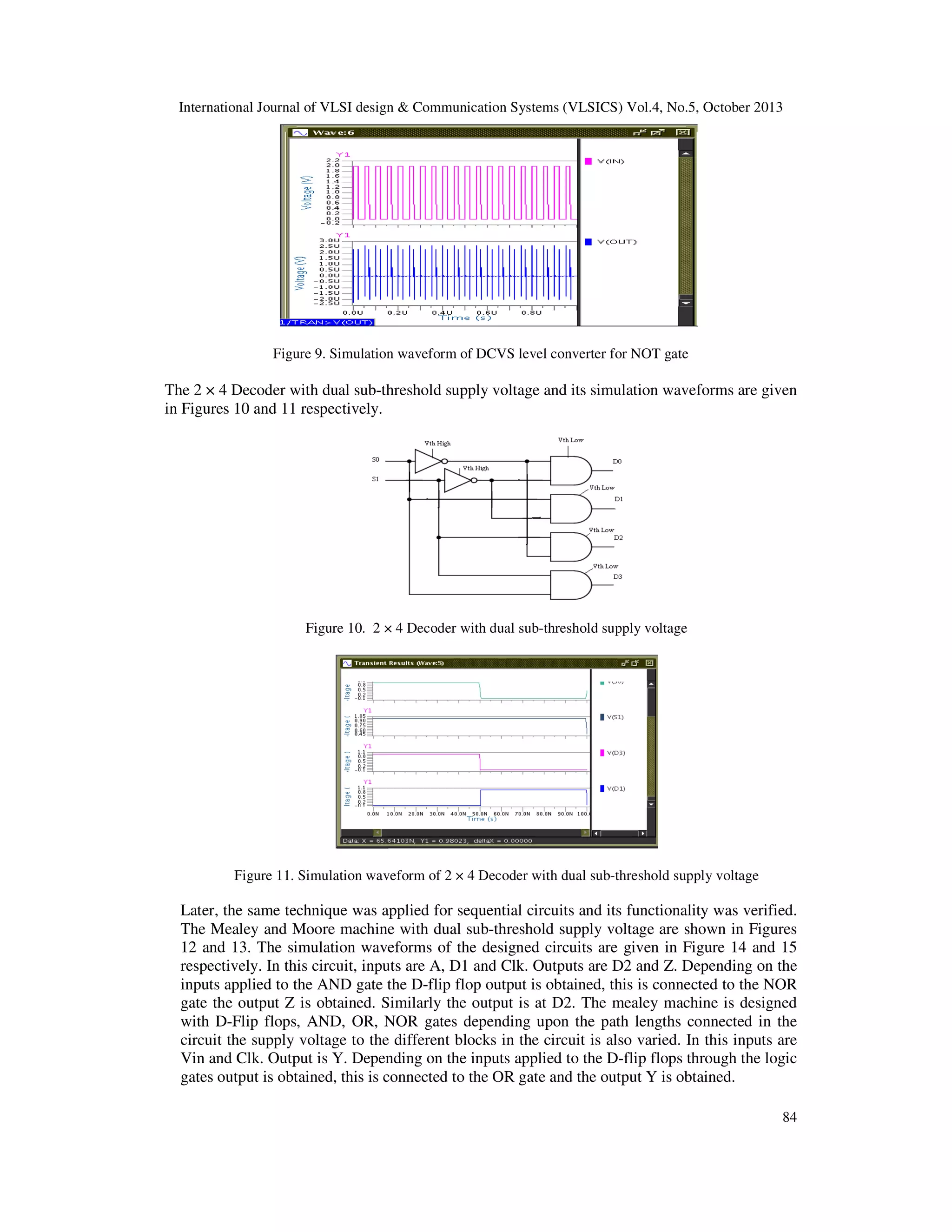
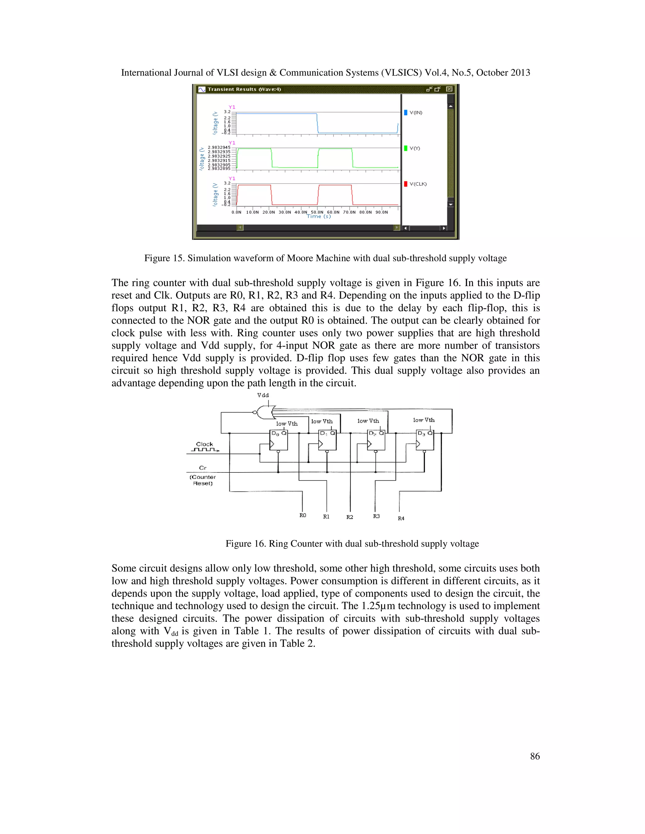
5. IMPLEMENTATION
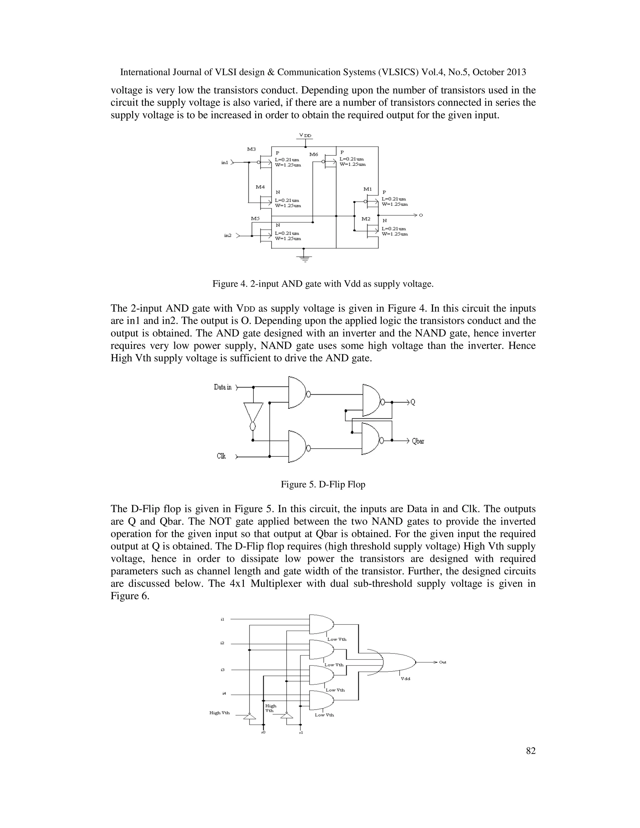
Any CMOS circuits can be designed by implementing the dual sub-threshold supply voltages
along with Vdd. The designed combinational circuits are decoder, 4x1 multiplexer and sequential
circuits are Moore and Mealey machine, ring counter. The logic gates are designed with CMOS
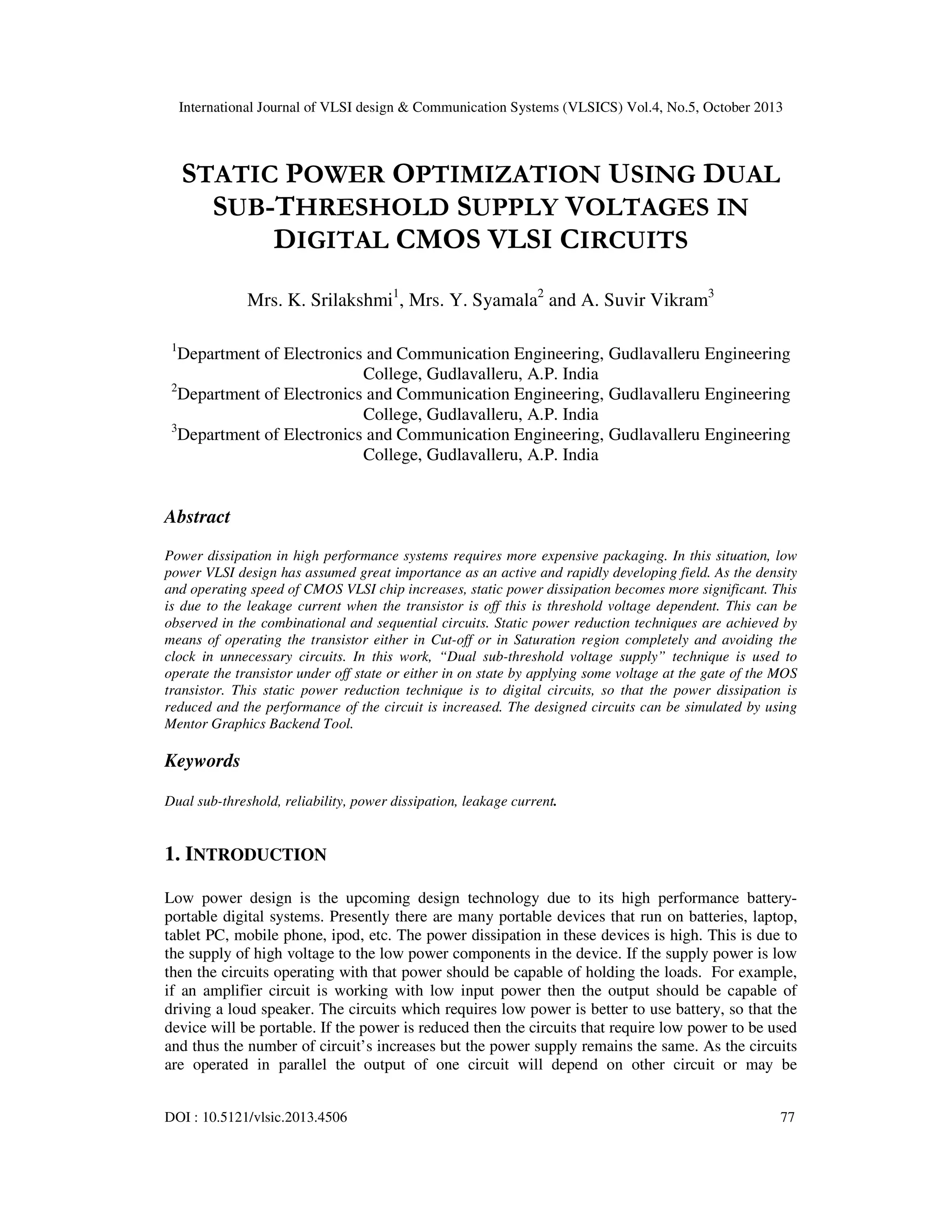
transistors, the gates are designed as shown below. The inverter with VDD as supply voltage is
given in Figure 1.
80](https://image.slidesharecdn.com/staticpoweroptimizationusingdualsub-thresholdsupplyvoltagesindigitalcmosvlsicircuits-131111204856-phpapp01/75/Static-power-optimization-using-dual-sub-threshold-supply-voltages-in-digital-cmos-vlsi-circuits-4-2048.jpg)
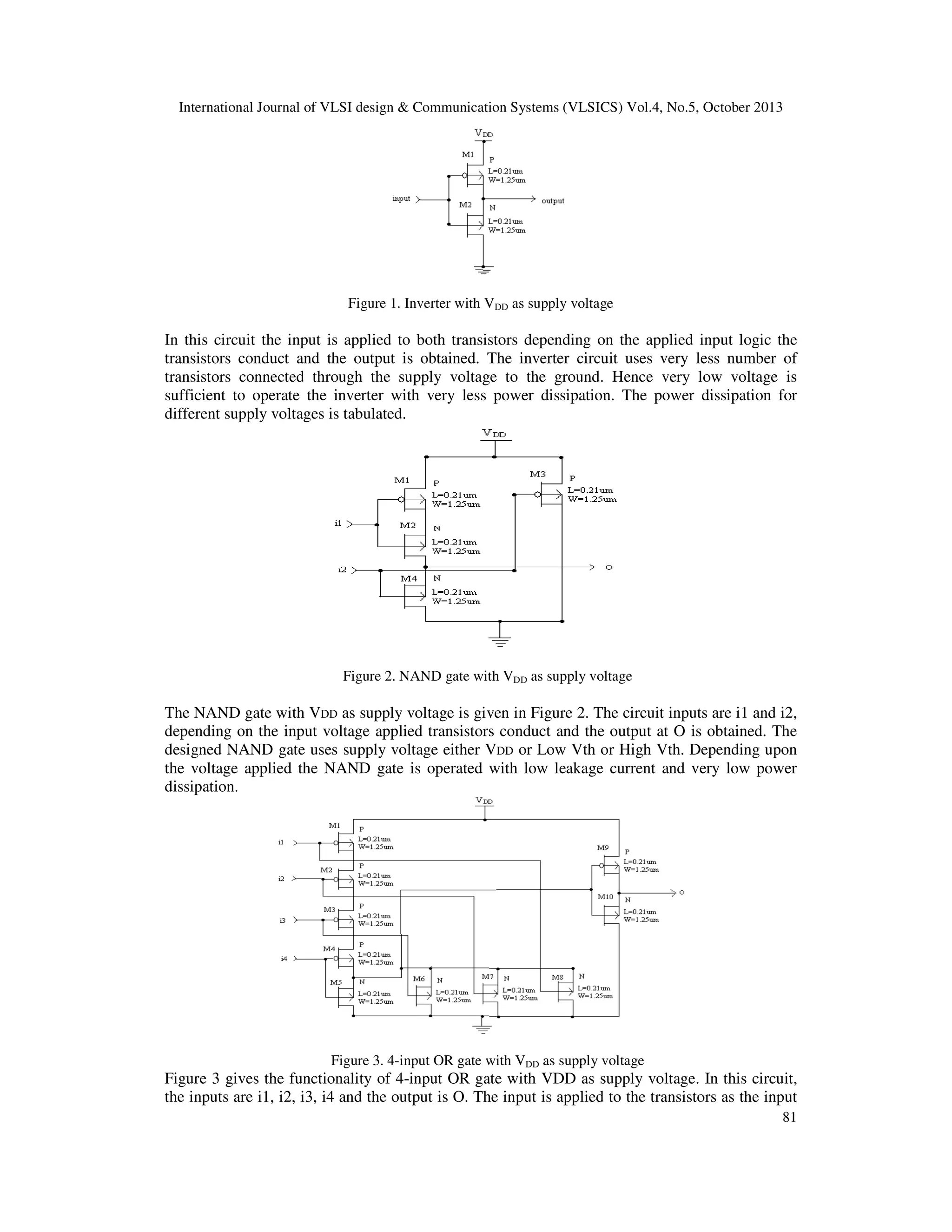
![International Journal of VLSI design & Communication Systems (VLSICS) Vol.4, No.5, October 2013
7. CONCLUSION
The power dissipation by using dual sub-threshold supply voltage along with VDD is less when
compared to the dual sub-threshold supply voltage without VDD. The power dissipation increases
while increasing the VDD supply voltage. The leakage power dissipation is high for very low
supply voltages due to the leakage current through the ground. This technique can be applied for
any CMOS digital circuits depending on number of components used. High supply voltages can
not be applied for these designed circuits. Hence this technique provides a better solution for the
low power devices.
REFERENCES
[1]
[2]
[3]
[4]
[5]
[6]
[7]
Kaushik Roy, Amit Agarwal, Chris H. Kim, Circuit Techniques for Leakage Reduction, LLC 2006.
Kaushik Roy, Saibal Mukhopadhyay and Hamid Mahmoodi-Meimand IEEE, Leakage Current
Mechanisms and Leakage Reduction Techniques in Deep-Submicrometer CMOS Circuits,
Contributed Paper, pp.315-318.
Shin’ichiro Mutoh , Yasuyuki Matsuya , Takahko Aoki and Junzo Yamada “1-V Power Supply
High-speed Digital Circuit Technology with Multithreshold-Voltage CMOS”, IEEE, vol. 30, August
1995, pp.847-848.
R. Gonzalez, B. M. Gordon, and M. A. Horowib. “Supply and threshold voltage scaling for low
power CMOS”, IEEE, Vol. 32, No. 8, August 1997.
L. Clark, R. Patel and T. Beatty, “Managing Standby and Active Mode Leakage Power in Deep
Sub-micron Design”, IEEE Circuits Devices Mag., vol. 21, no. 1, pp. 7–18, Jan./Feb. 2005.
Pankaj Pant, Rabindra K. Roy, and Abhijit Chatterjee “Dual-Threshold Voltage Assignment with
Transistor Sizing for Low Power CMOS Circuits”, IEEE 2001 pp.303-306.
Md.Asif Jahangir Chowdhury “An Efficient VLSI Design Approach to Reduce Static Power using
Variable Body Biasing”, World Academy of Science, Engineering and Technology 2012, pp. 262263.
Authors
Srilakshmi born at Karnataka. She completed her B.Tech degree from
JNTUK,
Kakinada, India in 2009, and M.Tech in 2011 from the JNTUK University in VLSI
System Design as specialization. She is currently working as a assistant professor in
Department of ECE in Gudlavalleru Engineering college, India. Her research interest
includes Low power design, VLSI design, and embedded design. She has been
published several papers in different various conferences.
Syamala born on Sept 14th 1980 in kavali, India. Obtained B.E degree from Bharatiyar
University, India in 2001. M.E degree in applied electronics from Anna University in
2005. In 2005, she joined as an assistant professor in Gudlavalleru Engineering College.
In 2011, she promoted as an Associate Professor in department of ECE, GEC, India.
She has been a member of IEEE, FIETE, ISTE, and MISTE. She has published several
papers in the area of VLSI. Her research interest includes VLSI design, digital design
and testing.
Suvir Vikram.A born in Vuyyuru, India. He has obtained his Bachelor degree in
Electronics and Communication from Newtons Institute of Engineering, Macherla in
2011. Presently he is pursuing his Masters degree in Embedded Systems of Electronics
and Communication in Gudlavalleru Engineering College, Gudlavalleru from 2011 to
2013 .He is interested in Low power VLSI design. He is currently working on a project
titled “Static Power Optmization using dual sub-threshold supply voltage in Digital
CMOS VLSI Circuits”as a partial fulfilment of his M.Tech degree.
88](https://image.slidesharecdn.com/staticpoweroptimizationusingdualsub-thresholdsupplyvoltagesindigitalcmosvlsicircuits-131111204856-phpapp01/75/Static-power-optimization-using-dual-sub-threshold-supply-voltages-in-digital-cmos-vlsi-circuits-12-2048.jpg)

The document discusses static power optimization techniques in digital CMOS VLSI circuits, focusing on the dual sub-threshold supply voltage method to reduce power dissipation. It highlights the importance of low power design for portable devices, the effects of leakage current, and various low power design techniques. The authors present the implementation of circuits designed using this technique and their simulations, demonstrating improvements in power efficiency and circuit performance.


![Vibe Coding vs. Spec-Driven Development [Free Meetup]](https://cdn.slidesharecdn.com/ss_thumbnails/vibecodingvsspecdrivendevelopment-251209105622-43f455e7-thumbnail.jpg?width=640&height=640&fit=bounds)


