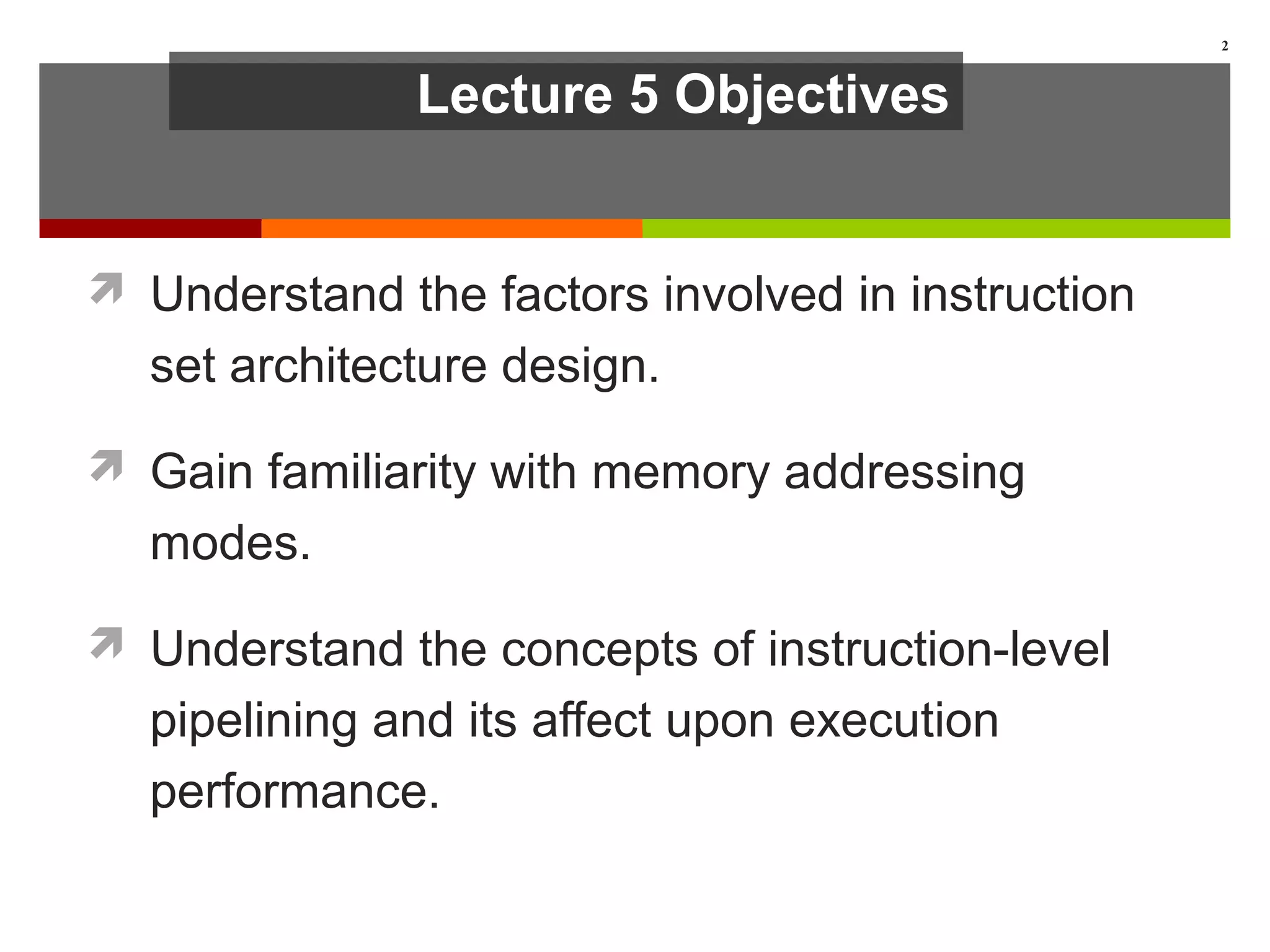
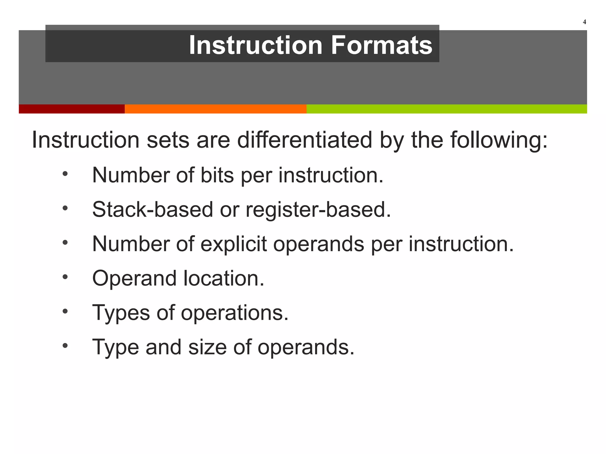
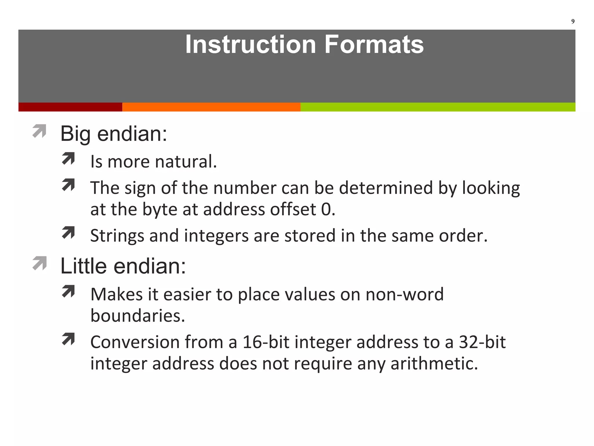
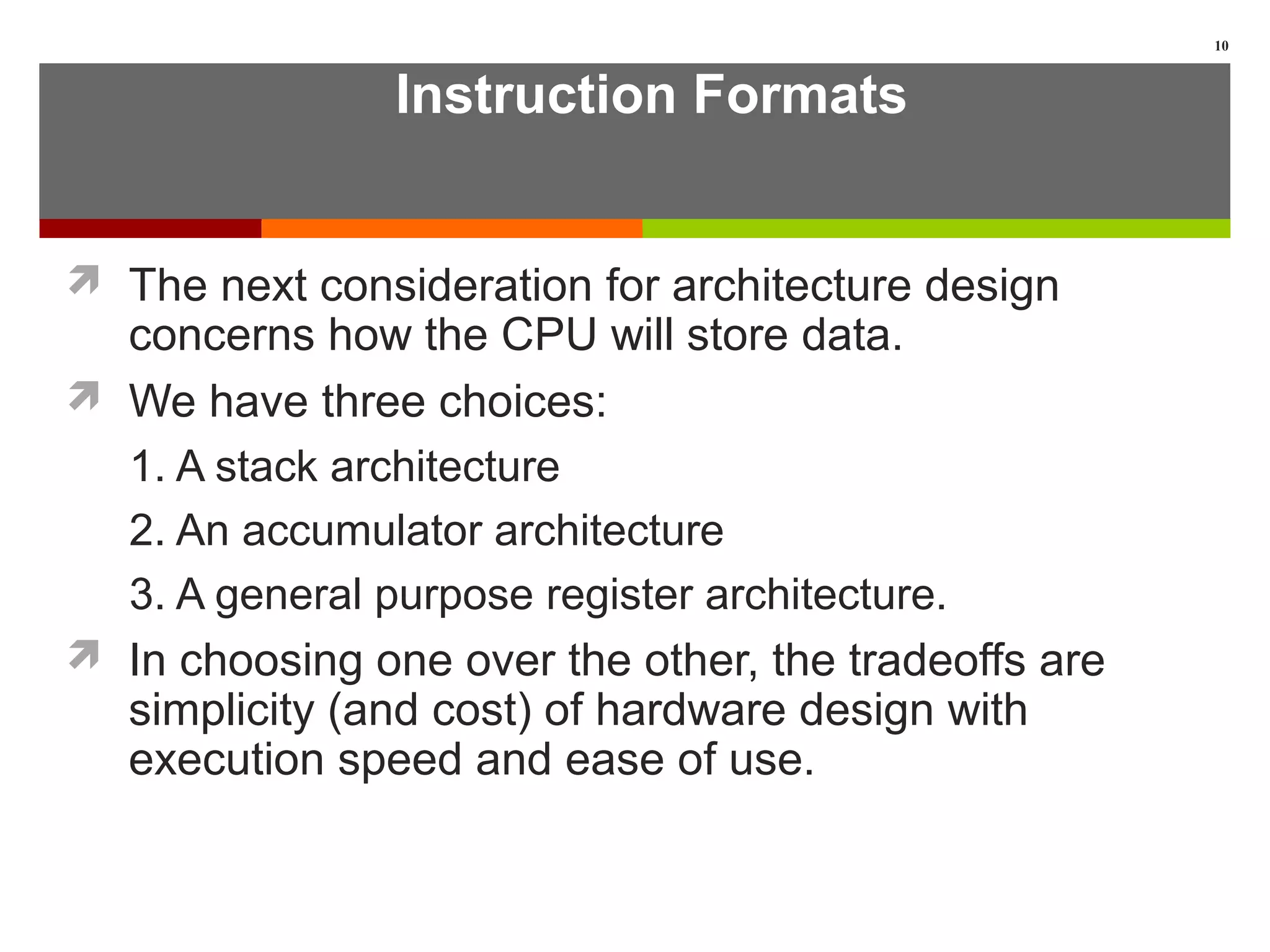
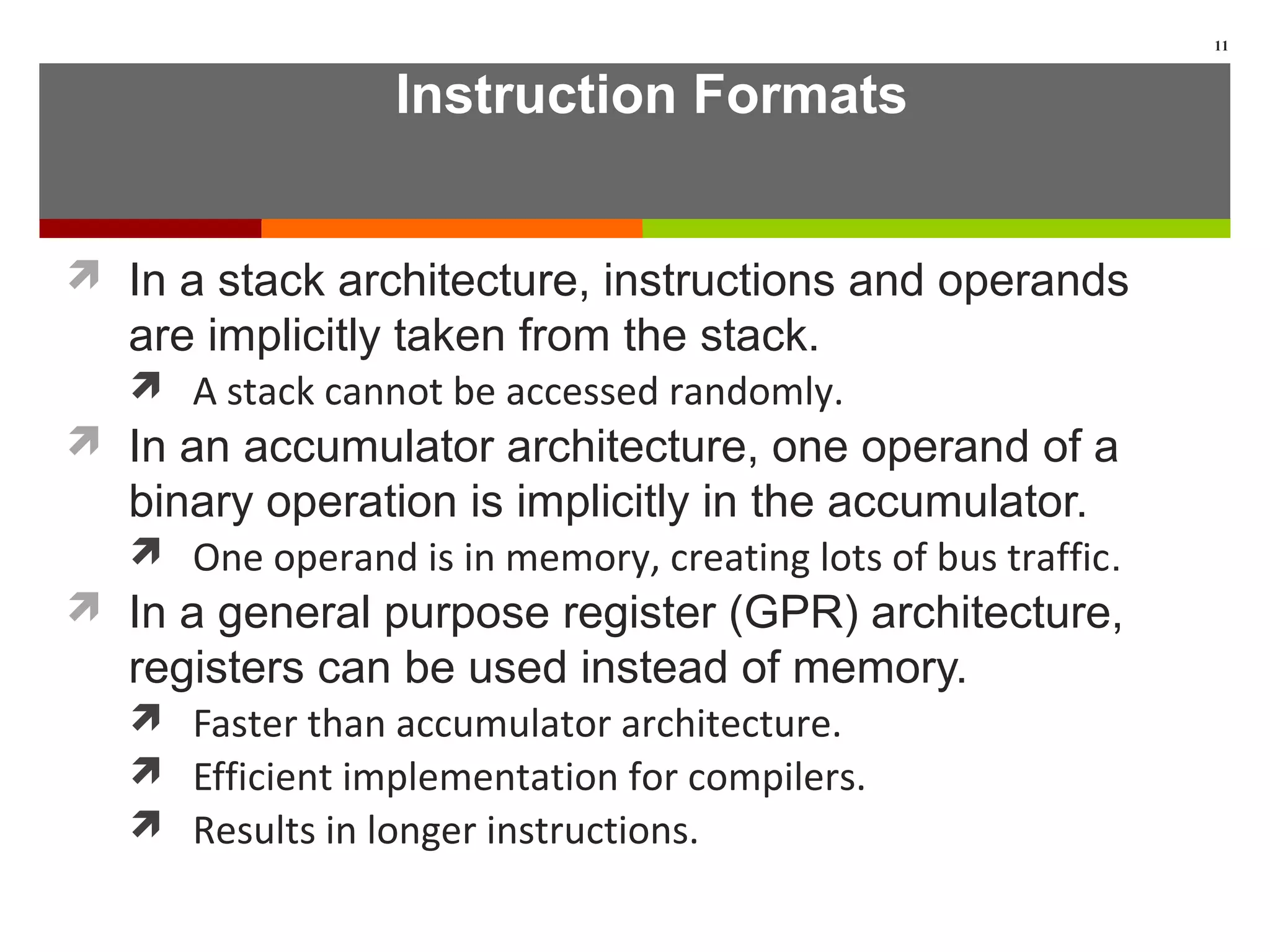
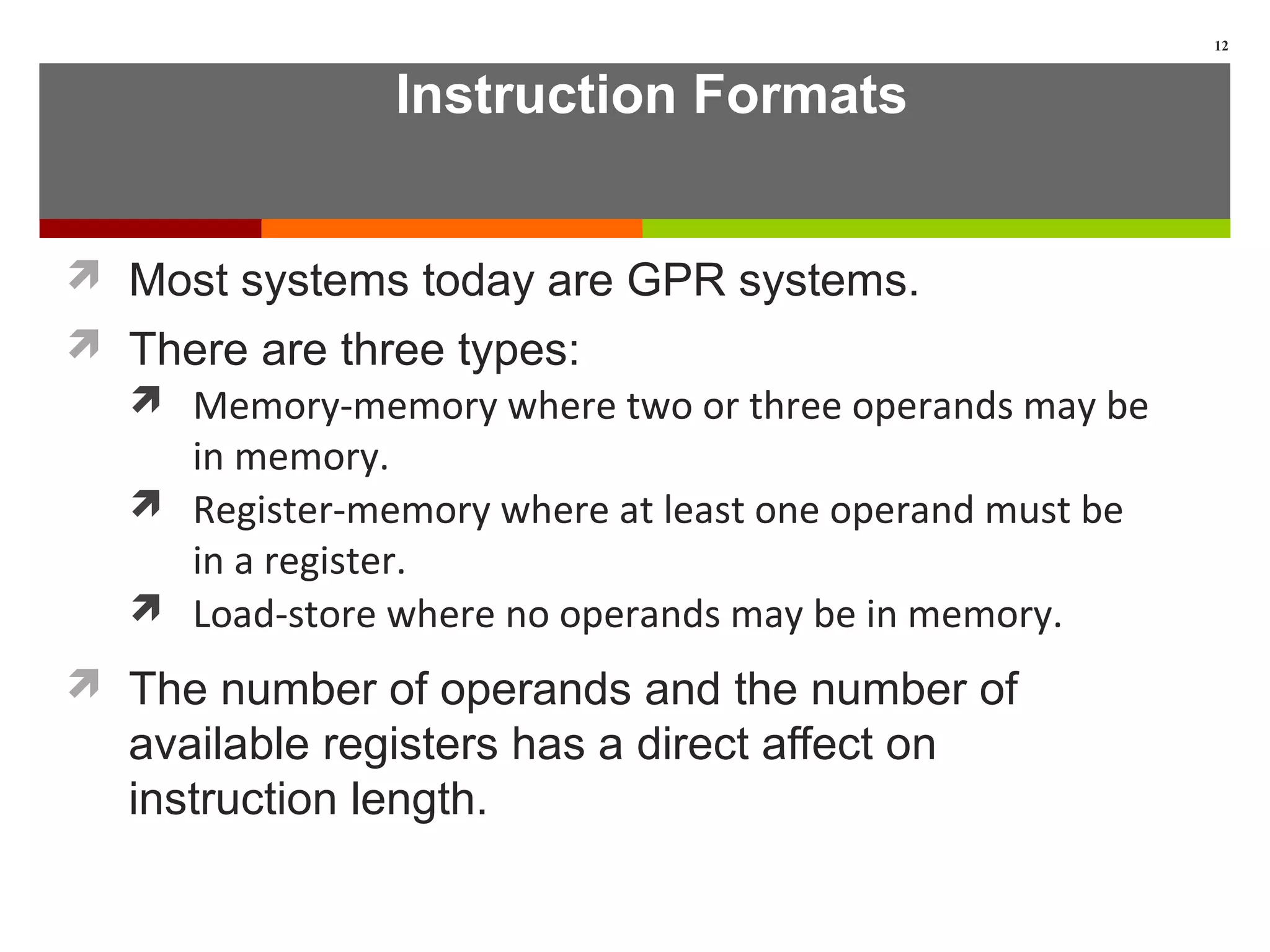
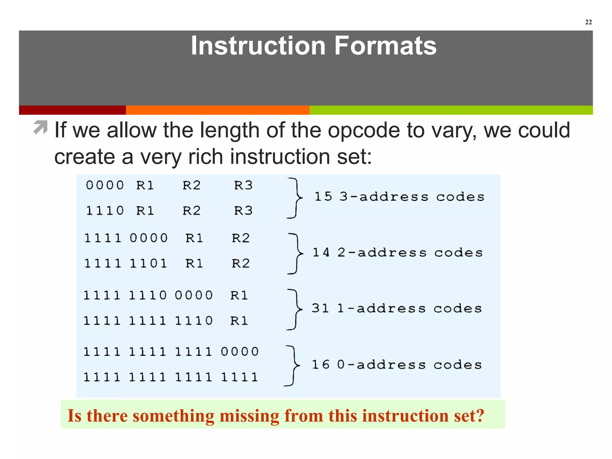
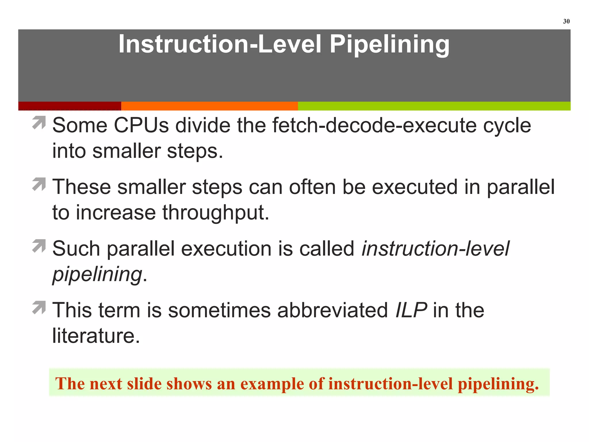
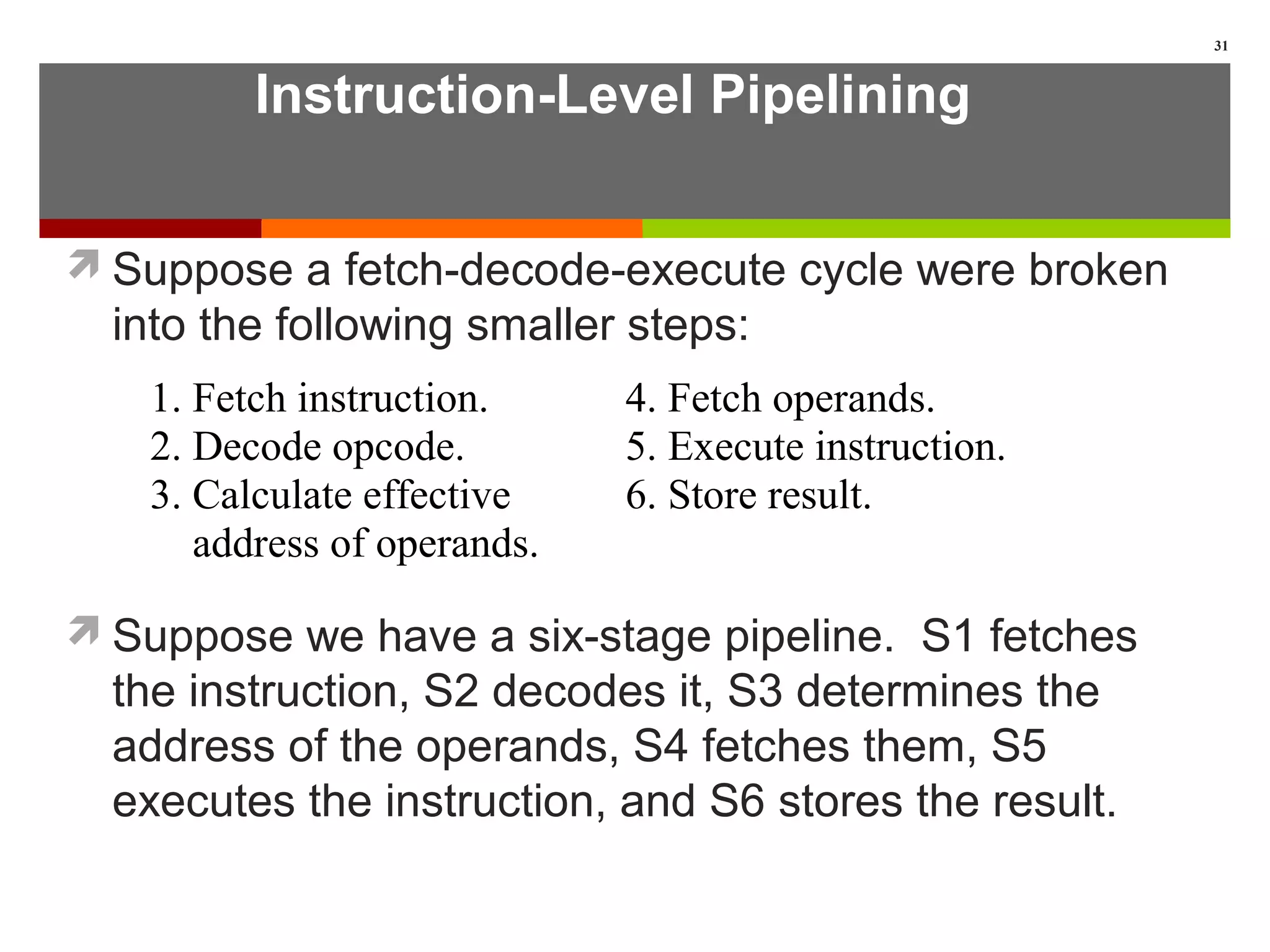
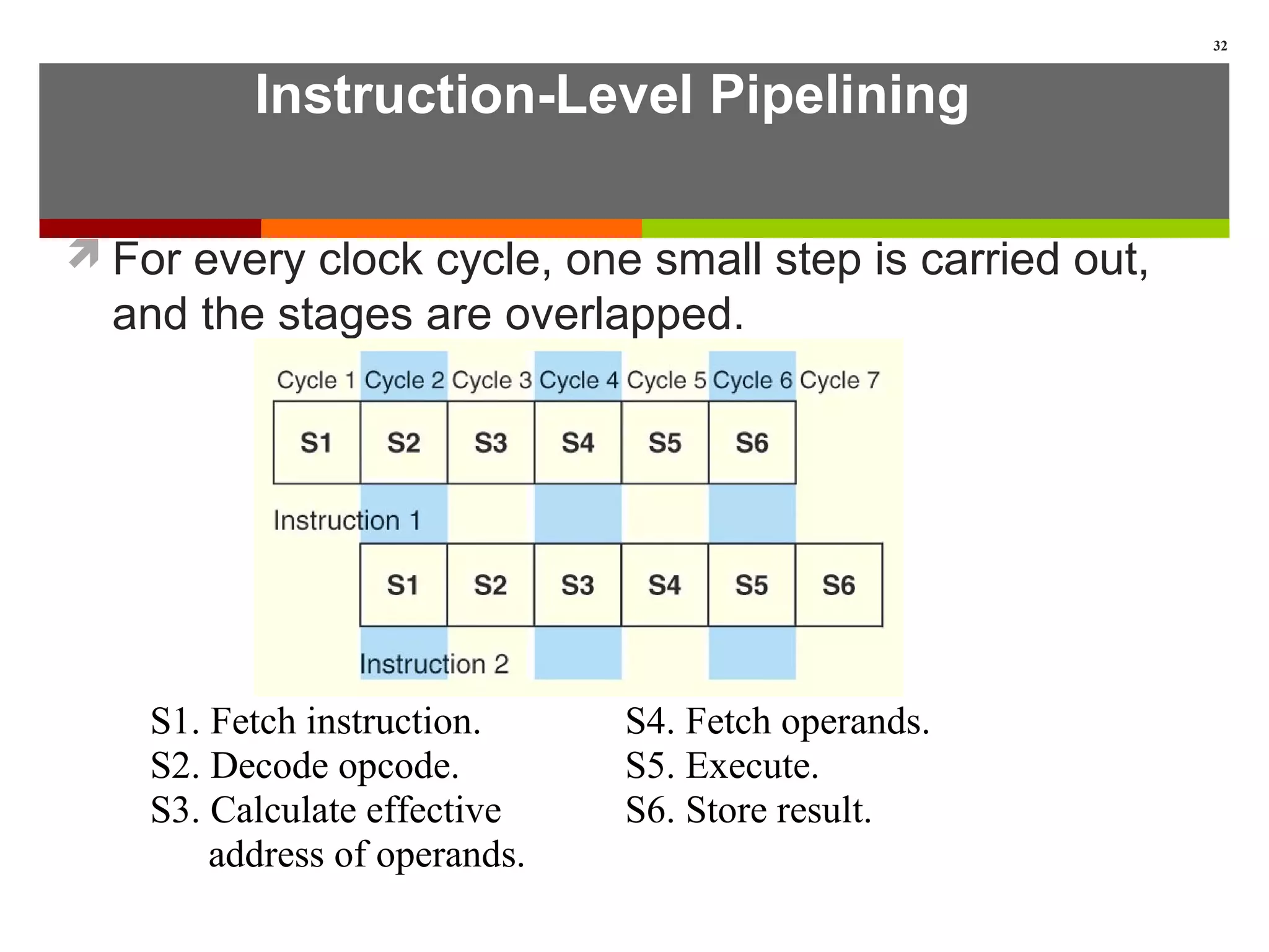
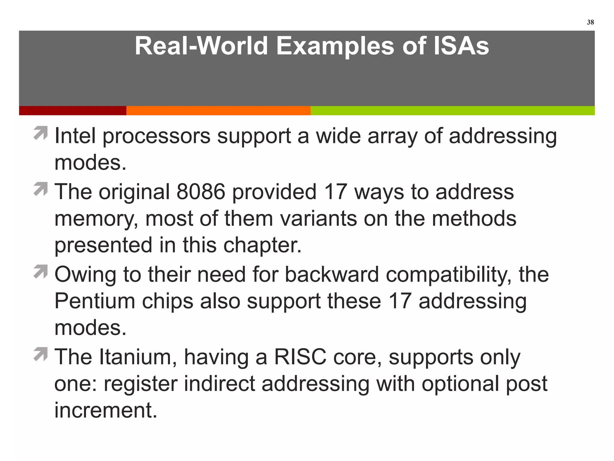
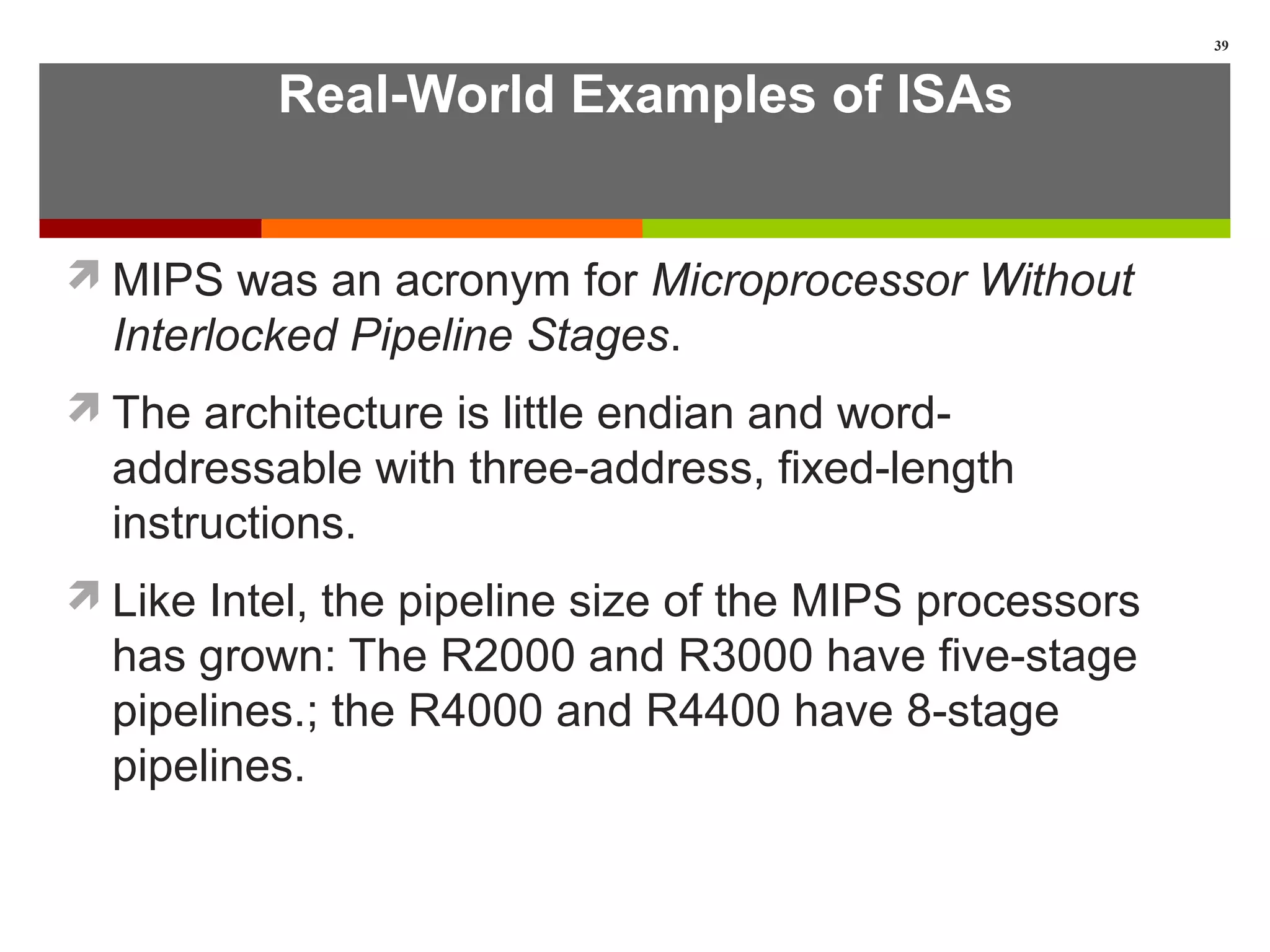
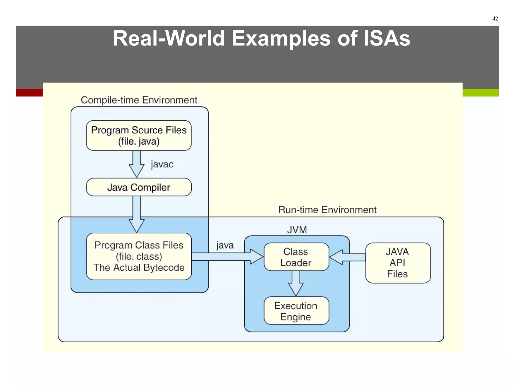
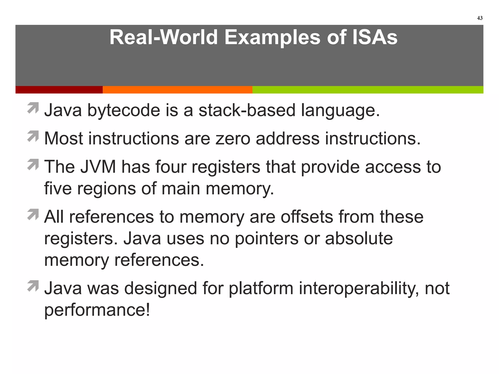
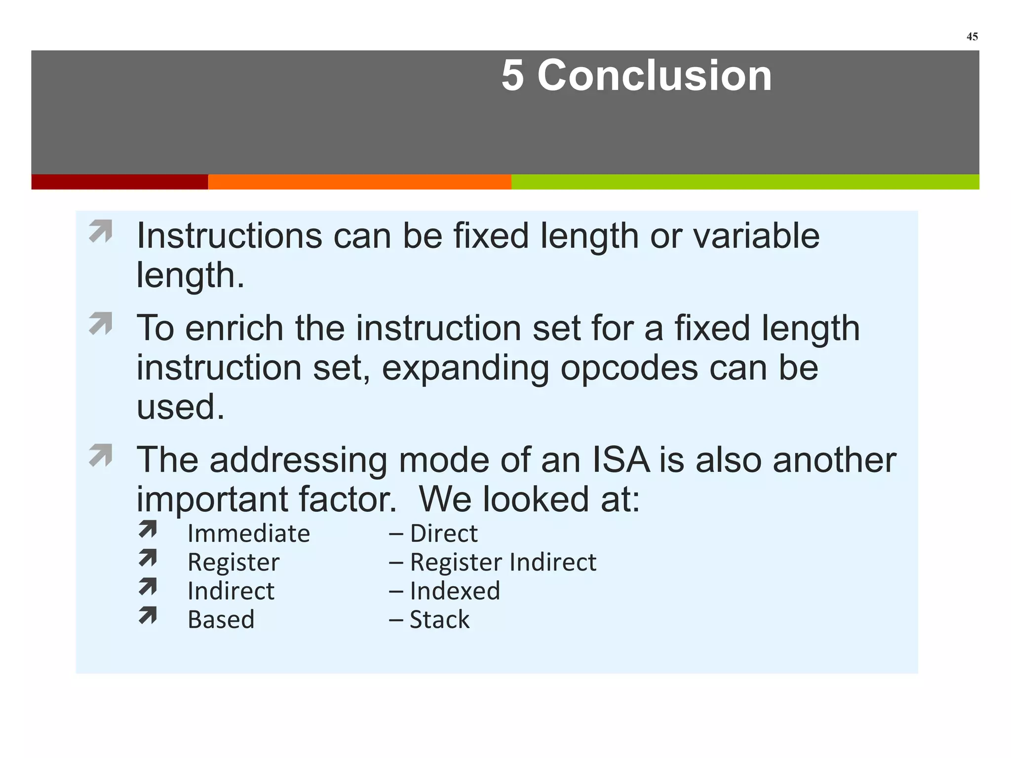
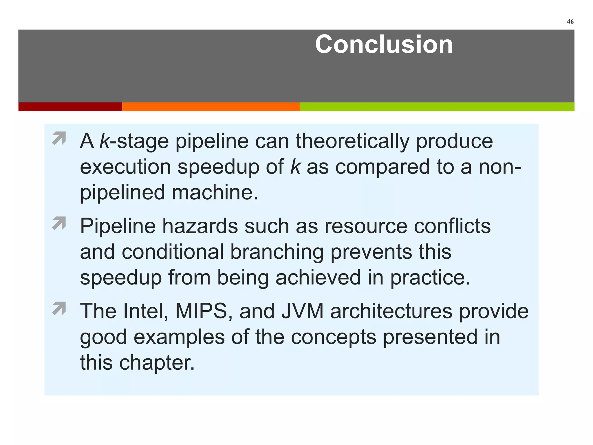
This lecture provides a detailed look at instruction set architectures (ISAs). It discusses instruction formats, including the number of operands, operand locations and types. It also covers addressing modes like immediate, direct, register, indirect and indexed. Additionally, it examines different approaches to storing data like stack, accumulator and general purpose register architectures. The lecture concludes by discussing instruction-level pipelining and examples of ISAs like Intel, MIPS and Java Virtual Machine.
This document provides an overview of memory organization and cache memory. It discusses the memory hierarchy from fast, small registers and caches closer to the CPU to larger, slower main memory and permanent storage like disks further away. Cache memory stores recently accessed data from main memory to speed up future accesses by taking advantage of temporal and spatial locality. Caches can be direct mapped, set associative, or fully associative and use different replacement policies like LRU when a block needs to be evicted.
Cache Memory Computer Architecture and organizationHumayra Khanum
Cache memory is a small, high-speed buffer located between the CPU and main memory that holds copies of frequently used instructions and data. It accelerates access to these items by keeping them closer to the CPU than main memory. There are separate caches for instructions and data, as well as a TLB cache that stores translated virtual addresses. Cache memory uses mapping techniques like direct mapping, set associative mapping, and fully associative mapping to determine where to store and retrieve items. Common replacement algorithms used when the cache is full are LRU, FIFO, LFU, and random selection.
Cache memory is a small, fast memory located close to the processor that stores frequently accessed data from main memory. When the processor requests data, the cache is checked first. If the data is present, there is a cache hit and the data is accessed quickly from the cache. If not present, there is a cache hit and the data must be fetched from main memory, which takes longer. Cache memory relies on principles of temporal and spatial locality, where frequently and nearby accessed data is likely to be needed again soon. Mapping functions like direct, associative, and set-associative mapping determine how data is stored in the cache. Replacement policies like FIFO, LRU, etc. determine which cached data gets replaced when new
Cache memory is a small, high-speed memory located between the CPU and main memory. It stores copies of frequently used instructions and data from main memory in order to speed up processing. There are multiple levels of cache with L1 cache being the smallest and fastest located directly on the CPU chip. Larger cache levels like L2 and L3 are further from the CPU but can still provide faster access than main memory. The main purpose of cache is to accelerate processing speed while keeping computer costs low.
Cache memory is a high-speed memory located between the CPU and main memory that acts as a buffer to improve access time. There are three types of cache mapping: direct mapping maps each memory block to a single cache line; associative mapping allows any memory block to be placed in any cache line; and set-associative mapping groups lines into sets and allows blocks to map to any line within a set. The performance of cache is determined by the hit ratio, which is the number of hits divided by the total number of memory accesses.
This document contains information about cache memory provided by multiple students:
- Cache memory is a fast type of volatile memory that stores frequently used data and programs to provide faster access for the CPU. It stores data temporarily until the computer is powered off.
- There are different levels of cache memory with L1 cache being the fastest and closest to the CPU. Cache mapping determines how data is stored in cache memory and there are three main types: direct mapping, associative mapping, and set associative mapping.
- When data is replaced in cache memory, different replacement algorithms are used to determine which data to remove. Write policies like write-through and write-back determine when written data is transferred from cache to main
This document discusses various aspects of computer memory systems including cache memory. It begins by defining key terms related to memory such as capacity, organization, access methods, and physical characteristics. It then covers cache memory in particular, explaining the basic concept of caching as well as aspects of cache design like mapping, replacement algorithms, and write policies. Examples of cache configurations from different processor models over time are also provided.
Cache memory is a small, fast memory located between the CPU and main memory that temporarily stores frequently accessed data. It improves performance by providing faster access for the CPU compared to accessing main memory. There are different types of cache memory organization including direct mapping, set associative mapping, and fully associative mapping. Direct mapping maps each block of main memory to only one location in cache while set associative mapping divides the cache into sets with multiple lines per set allowing a block to map to any line within a set.
This document discusses cache memory and provides details on its characteristics and operation. It begins by describing the memory hierarchy and how cache fits within it. It then covers the key characteristics of cache memory, including that it is small, fast memory located close to the processor. The document explains how cache works by checking if requested data is present before accessing slower main memory if there is a miss. Overall, the document provides an overview of cache memory fundamentals.
Cache memory is used to improve processor performance by making main memory access appear faster. It works based on the principle of locality of reference, where programs tend to access the same data/instructions repeatedly. A cache hit provides faster access than main memory, while a miss requires retrieving data from main memory. Caches use mapping functions like direct, associative, or set-associative mapping to determine where to place blocks of data from main memory.
This document discusses the key characteristics of computer memory, including location, capacity, unit of transfer, access methods, performance, physical type, physical characteristics, and organization. It covers different types of memory like CPU registers, main memory, cache, disk, and tape. The different access methods like sequential, direct, random, and associative access are explained. The memory hierarchy and performance aspects like access time, memory cycle time, and transfer rate are defined. Factors like cache size, mapping function, replacement algorithm, write policy, block size that impact cache performance are also summarized.
Cache memory is a small, fast memory located between the CPU and main memory. It stores copies of frequently used instructions and data to accelerate access and improve performance. There are different mapping techniques for cache including direct mapping, associative mapping, and set associative mapping. When the cache is full, replacement algorithms like LRU and FIFO are used to determine which content to remove. The cache can write to main memory using either a write-through or write-back policy.
Cache memory is a small, fast memory located close to the processor that stores frequently accessed instructions and data. There are typically three levels of cache (L1, L2, L3) with L1 being the smallest and fastest cache located directly on the CPU chip. The performance of a cache is measured by its hit ratio, with a higher hit ratio indicating better performance as the CPU is less likely to access the slower main memory.
Caches are commonly used in high-performance computing to improve performance. However, high-performance computing applications often perform poorly on computer architectures that employ caches, unless the application software is specifically tuned to exploit the caches. There are several basic design elements that differentiate cache architectures, including the cache size, mapping function, replacement algorithm, write policy, line size, and number of cache levels. The replacement algorithm determines which block of data to remove from the cache when a new block needs to be added.
The document discusses cache design and organization. It describes how caches work, sitting between the CPU and main memory to provide fast access to frequently used data. The key aspects covered include cache size, block size, mapping techniques, replacement algorithms, write policies, and the evolution of cache hierarchies in processors like the Pentium IV with multiple levels of on-chip and off-chip caches.
The Presentation introduces the basic concept of cache memory, its introduction , background and all necessary details are provided along with details of different mapping techniques that are used inside Cache Memory.
This document describes a student's project to design an energy efficient cache memory using Verilog HDL. It presents the background and motivation, including that write-through caches consume a lot of energy due to increased access at lower levels. The proposed work introduces a way-tagged cache architecture to reduce energy consumption. Simulation results show energy savings of the proposed cache compared to a conventional cache for various operations like reset, data load, read and write hits/misses. The conclusion is that the way-tagged cache adds new components to L1 cache but remains inbuilt with the processor, with area overhead as a drawback.
Cache memory is a small, fast memory located between the CPU and main memory that stores copies of frequently used instructions and data. It accelerates computer speed while keeping costs low. When the CPU requests data, the cache is checked first for a cache hit before accessing the slower main memory. If the data is not found in cache, a cache miss occurs and the data must be retrieved from main memory, which is slower. Replacement algorithms like LRU determine which cached data to replace when new data must be added to a full cache.
This document discusses cache memory and its characteristics. It begins by defining cache memory as a smaller, faster memory located close to the CPU that stores copies of frequently accessed data from main memory. This is done to achieve higher CPU performance by allowing faster access to cached data compared to main memory. The document then covers various characteristics of cache memory like location, capacity, unit of transfer, access methods, performance, organization, mapping functions, replacement algorithms, and write policies. Diagrams are included to illustrate cache read operations and different mapping approaches.
Cache coherence refers to maintaining consistency between data stored in caches and the main memory in a system with multiple processors that share memory. Without cache coherence protocols, modified data in one processor's cache may not be propagated to other caches or memory. There are different levels of cache coherence - from ensuring all processors see writes instantly to allowing different ordering of reads and writes. Cache coherence aims to ensure reads see the most recent writes and that write ordering is preserved across processors. Directory-based and snooping protocols are commonly used to maintain coherence between caches in multiprocessor systems.
Cache is a small, fast memory located close to the CPU that stores frequently accessed data from main memory. It reduces access time by storing instructions and data locally. There are separate instruction and data caches. A cache hit occurs when data is found in cache, while a cache miss requires loading data from main memory, increasing access time. Caches are organized into lines and sets, and use policies like LRU for replacing data on a miss. The hit rate and miss penalty determine average memory access time.
Interleaved memory is a design that spreads memory addresses across multiple memory banks to compensate for the relatively slow speed of DRAM. It increases bandwidth and improves performance by allowing different modules to be accessed independently and in parallel by different processing units like a CPU and hard disk. There are two address formats for interleaved memory: low order interleaving which spreads addresses across banks, and high order interleaving which uses high order bits as the module address.
Associative memory, also known as content-addressable memory (CAM), allows data to be searched based on its content rather than its location. It consists of a memory array, argument register (containing the search word), key register (specifying which bits to compare), and match register (indicating matching locations). All comparisons are done in parallel. Associative memory provides faster searching than conventional memory but is more expensive due to the additional comparison circuitry in each cell. It is well-suited for applications requiring very fast searching such as databases and virtual memory address translation.
There are three main methods for mapping memory addresses to cache addresses: direct mapping, associative mapping, and set-associative mapping. Direct mapping maps each block of main memory to a single block in cache in a one-to-one manner. Associative mapping allows any block of main memory to be mapped to any block in cache but requires tag bits to identify blocks. Set-associative mapping groups cache blocks into sets, with a main memory block mapped to a particular set and then flexibly to a block within that set, providing more flexibility than direct mapping but less complexity than full associative mapping.
Cache memory is a small amount of fast SRAM located between the CPU and main memory that stores frequently accessed data. When the CPU requests data, the cache memory is checked first and if the data is present it can be accessed much faster than main memory. If the data is not in cache memory, it is retrieved from main memory which is slower but larger DRAM. Modern processors use a multi-level cache system with multiple cache levels (L1, L2, etc.) checked sequentially to improve performance.
- A key objective of computer systems is achieving high performance at low cost, measured by price/performance ratio.
- Processor performance depends on how fast instructions can be fetched from memory and executed.
- Caches improve performance by storing recently accessed data from main memory closer to the processor, reducing access time compared to main memory. This can increase hit rates but requires managing cache misses and write policies.
Fixed-point and floating-point numbers can be represented in computers using binary numbers. Floating-point numbers represent numbers in scientific notation with a sign, mantissa, and exponent. In 8-bit floating point, numbers use 1 bit for sign, 3 bits for exponent, and 4 bits for mantissa, such as 0.001 x 21 = 2.25. Larger precision formats such as 32-bit and 64-bit floating point according to the IEEE standard use more bits for exponent and mantissa.
A tree is a hierarchical data structure where items are arranged in a sorted sequence. It represents relationships between data items. A tree has a root node at the top with child nodes branching out connected by edges. Each node stores data and links to other nodes. The level of a node indicates its depth from the root with the root being level 0. Siblings are nodes that share the same parent. Leaf nodes have no children while non-terminal nodes have children. The degree of a node is the number of subtrees extending from it.
The document discusses binary trees and various operations on them. It defines what a binary tree is composed of (nodes with values and pointers to left and right children). It describes tree traversals like preorder, inorder and postorder that output the nodes in different orders. It explains two common search strategies - depth-first search (DFS) and breadth-first search (BFS) - and provides examples of how they traverse a sample tree. It also briefly discusses operations like finding the minimum/maximum element, inserting a new element, and deleting an existing element from the binary search tree.
The document discusses the different addressing modes of the 8086 processor. It describes 6 main addressing modes - register, immediate, memory, port, relative, and implied. The memory addressing mode has several sub-types including direct, register indirect, based, indexed, based indexed, and string addressing modes which specify how the effective address of the memory operand is calculated using segment registers and offsets.
1) Trees are hierarchical data structures that store data in nodes connected by edges. They are useful for representing hierarchical relationships.
2) Binary search trees allow quick search, insertion, and deletion of nodes due to the organizational property that the value of each node is greater than all nodes in its left subtree and less than all nodes in its right subtree.
3) Common tree traversal algorithms include preorder, inorder, and postorder traversals, which visit nodes in different orders depending on whether the left/right children or root is visited first.
This document discusses trees as a data structure. It defines trees as structures containing nodes where each node can have zero or more children and at most one parent. Binary trees are defined as trees where each node has at most two children. The document discusses tree terminology like root, leaf, and height. It also covers binary search trees and their properties for storing and searching data, as well as algorithms for inserting and deleting nodes. Finally, it briefly discusses other types of trees like balanced search trees and parse trees.
This document defines and describes trees and graphs as non-linear data structures. It explains that a tree is similar to a linked list but allows nodes to have multiple children rather than just one. The document defines key tree terms like height, ancestors, size, and different types of binary trees including strict, full, and complete. It provides properties of binary trees such as the number of nodes in full and complete binary trees based on height.
The document discusses machine instruction sets and their design. It covers the following key points:
- Machine instructions specify the operations the processor executes. The collection of instructions is called the instruction set.
- Instructions contain fields like operation codes, source/destination operands, and next instruction references.
- Instruction formats vary in the number of addresses/operands per instruction, from zero to three or more. More addresses generally means more complex instructions but simpler programs.
- Common instruction types include arithmetic, logic, memory, test, and branch instructions. Instruction design involves balancing programmer needs with processor implementation.
This document discusses different addressing modes and RISC and CISC microprocessors. It defines eight addressing modes: register, register indirect, immediate, direct, indirect, implicit, relative, and index addressing modes. It provides examples for each mode. The document also defines RISC and CISC architectures, noting that RISC uses simple instructions that perform in one clock cycle while CISC uses more complex instructions that can perform multiple operations. It compares the two approaches using multiplying two numbers as an example.
The document discusses machine instruction characteristics and instruction sets. It begins by describing the typical elements of a machine instruction, which include an operation code, source operand reference(s), result operand reference, and next instruction reference. It then discusses the types of locations that can hold operands, including memory, registers, immediate values, and I/O devices. The document provides examples of instructions with different numbers of addresses (zero, one, two, and three addresses) and how programs can be written using each type. Overall, the document provides an overview of the essential components of machine instructions and instruction sets.
The document provides information about a class presentation on bus structures. It discusses parallel and serial communication, synchronous and asynchronous buses, basic protocol concepts, and bus arbitration. Specifically, it defines parallel and serial communication, explains the differences between synchronous and asynchronous buses, describes the basic components of a bus transaction including requests and data transfer, and outlines different approaches to bus arbitration including daisy chain, centralized parallel arbitration, and polling. The presentation aims to provide both a review of key bus topics and a practical exposure to the concepts through examples and diagrams.
(246431835) instruction set principles (2) (1)Alveena Saleem
The document discusses instruction set architecture principles including what an instruction set is, how instructions are represented and classified, and different types of instruction sets. It covers topics like register-based machines, addressing modes, common instruction types, and how the instruction set affects compiler design and register allocation.
This document discusses computer instructions and addressing modes. It defines an instruction as consisting of an opcode and address. Common instructions like LOAD, STORE, ADD, and SUB are described. Addressing modes like immediate, direct, indirect, register, and displacement are explained with diagrams. Factors that influence instruction set design like instruction length, encoding schemes, and addressing modes are covered at a high level. The goal is to optimize for speed of fetching and decoding instructions while supporting required functionality.
The document discusses instruction set architecture (ISA), which defines the interface between software and hardware. It describes ISA as specifying storage locations, operations, and how to invoke and access them. The document then compares ISA to human language and discusses program compilation. It outlines the basic instruction execution model of fetching, decoding, executing and writing instructions. The document also describes different types of instruction sets like stack, accumulator and register-set architectures. Finally, it contrasts complex instruction set computers (CISC) with reduced instruction set computers (RISC).
This document provides an overview of instruction sets and assembly language programming. It discusses different types of instruction sets including CISC, RISC, and hybrid approaches. The document then describes the classification of instruction sets into categories like data movement, compare, branch, arithmetic, logic, and bit manipulation instructions. It also covers instruction formats, addressing modes, operand sizes, comments, labels and examples of assembly language instructions.
An instruction code consists of an operation code and operand(s) that specify the operation to perform and data to use. Operation codes are binary codes that define operations like addition, subtraction, etc. Early computers stored programs and data in separate memory sections and used a single accumulator register. Modern computers have multiple registers for temporary storage and performing operations faster than using only memory. Computer instructions encode an operation code and operand fields to specify the basic operations to perform on data stored in registers or memory.
This document provides an overview of various types of registers used in microprocessors. It discusses system registers, status registers, pointer registers, index registers, hardware registers, instruction registers, control registers, memory management registers, segment registers, shift registers, stack registers, test registers, task registers, accumulator registers, EFLAGS registers, base address registers, and other specialized registers. The document aims to describe the purpose and function of different categories of registers within microprocessors.
Here are the steps to launch Microsoft Visual Studio 2008 and create a project to edit the program P 2-1:
1. Launch Microsoft Visual Studio 2008.
2. Click "File" -> "New" -> "Project".
3. In the "New Project" dialog box, select "Visual C++" in the left pane and "Win32 Console Application" in the middle pane.
4. Click "OK".
5. In the "Win32 Application Wizard" dialog box, enter a name for the project (e.g. "AssemblyProgram") and click "OK".
6. This will create a new empty project in Visual Studio.
7. Right click on the
This document discusses different addressing modes used in microprocessor instructions. It begins by explaining the importance of understanding addressing modes for efficient software development. It then provides objectives for the chapter, which are to explain each data and program memory addressing mode, how to use them to form assembly statements, and how to select the appropriate mode for a given task. The document goes on to describe various data addressing modes like register, immediate, direct, displacement, indirect, base-plus-index, relative, and scaled-index. It also covers program memory addressing modes like direct, relative, and indirect. Examples are provided to illustrate how each mode works.
This document provides information about a computer architecture course taught at Velammal Engineering College. The course is aimed at teaching students the basic structure and operations of a computer. It will cover topics like the ALU, pipelined execution, parallelism, memory hierarchies, and virtual memory. The course outcomes include discussing computer basics, designing an ALU, analyzing pipelining and parallel architectures, and examining memory systems. The syllabus is divided into 5 units covering basic computer structure, arithmetic, processors, parallelism, and memory/I/O systems. Textbooks and an introduction to the course are also included.
INTEL x86 AND ARM DATA TYPES
⦁ Are instructions set architecture
⦁ Change code into instructions a processor can understand and execute.
⦁ Determines which operating systems and apps to run.
The document discusses microprocessors, their architecture, instructions, operations, interfacing and the 8085 and 8086 microprocessors. It provides details on the functional blocks, registers, addressing modes, procedures, calling conventions, and stack usage of the 8086 microprocessor. It also describes various assembler directives, operators, and concepts like logical segments, procedures, and passing parameters in registers vs memory for procedures.
The document describes the von Neumann architecture, including its main components: main memory, arithmetic logic unit (ALU), control unit, CPU registers, and I/O equipment. The CPU consists of registers like the program counter, instruction register, and memory address register. The control unit interprets instructions and causes them to execute. Main memory stores both instructions and data, while the ALU performs arithmetic operations. I/O equipment is controlled by the control unit to input and output data.
This document discusses the differences between RISC and CISC instruction set architectures. RISC uses simple, fixed-length instructions that can execute in one cycle, while CISC uses more complex, variable-length instructions that may take multiple cycles. Key differences include RISC having fewer instructions, registers, and addressing modes compared to CISC, which aims to support high-level languages with a wider range of instructions. Branching, condition codes, and instruction formats are also covered.
The CPU is made up of 3 major parts: the register set, control unit, and arithmetic logic unit. The register set stores intermediate values during program execution. The control unit generates control signals and selects operations for the ALU. The ALU performs arithmetic and logic operations. Computer architecture includes instruction formats, addressing modes, instruction sets, and CPU register organization. Registers are organized in a bus structure to efficiently transfer data and perform microoperations under control of the control unit. Common instruction fields are the operation code, address fields, and addressing mode fields. Instructions can be classified by the number of address fields as zero-address, one-address, two-address, or three-address instructions. Common addressing modes specify how operands
The document discusses basic logic operations and logic gates. It explains that logic operations like AND, OR, and XOR can be implemented using logic gates and combined to perform more complex functions. Some common logic functions mentioned are comparison, arithmetic, coding, decoding, data selection, storage, and counting. Logic gates take binary inputs and produce binary outputs based on truth tables that define the logic operations.
This document covers digital circuitry topics including number systems, digital waveforms, pulse characteristics, waveform characteristics, and timing diagrams. It defines positive and negative pulses, and describes pulse parameters like rise time, fall time, pulse width, and amplitude. Periodic and non-periodic waveforms are discussed as well as frequency, period, and duty cycle. Timing diagrams are introduced as a way to synchronize digital signals with a clock waveform where each clock interval represents one bit. Examples are provided to demonstrate calculating pulse characteristics and drawing timing diagrams.
This document provides information about a course on digital circuitry, including required materials, assessment details, and contact information for the instructor. It discusses the textbook, simulation software, and additional recommended resources. Coursework will be 40% of the grade and an exam will make up the remaining 60%. Students should contact their class representative for any questions.
This document outlines the modules, activities, and assessments for an IS 151 course on digital circuits and logic design. Over 15 weeks, topics will include digital and binary concepts, number systems, logic gates and functions, Boolean algebra, Karnaugh maps, combinational logic, sequential logic elements like latches and flip-flops, finite state machines, and programmable logic devices. Assessment will include laboratory work, assignments, tests, and a final laboratory exercise on designing a Gray code counter.
This document contains 5 questions related to binary, hexadecimal, and decimal number conversions as well as calculating memory size needed for storing a film. Question 1 asks to convert between base 10, 2, and 16. Question 2 asks for the ASCII code for a word. Question 3 asks to write decimal fractions in binary. Question 4 asks to write positive and negative numbers in 6-bit two's complement binary form. Question 5 asks to calculate the memory needed in gigabytes for a film with given frame size, bit depth, frame rate, and length.
This document provides instructions for an assignment in a class on the MARIE assembly language. Students must complete 4 programming problems in groups of at most 2 people by writing MARIE programs, assembling them, and testing them using a MARIE simulator. They are to submit a zip file of their assembly code for each question, which includes writing loops to multiply numbers with repeated addition, an if/else statement to multiply or subtract values of variables x and y, adding the first 10 numbers, and subtracting 2 numbers input from the keyboard.
The document provides an overview of the components and architecture of the MARIE computer system, which was designed to illustrate basic computer concepts. It describes the CPU, registers, memory, bus, instruction set, and fetch-decode-execute cycle. The MARIE CPU has 7 registers, including the accumulator, program counter, and instruction register. It uses a 16-bit instruction format. Example load and add instructions are shown in register transfer language to demonstrate how instructions are executed as a series of microoperations. Interrupts can alter the execution cycle by adding an additional "process interrupt" step.
The document discusses data representation in computer systems. It begins by explaining that computers use the binary system for logic and arithmetic because it is easy to implement in electronics and switches. It then discusses how integers, floating point numbers, and Boolean logic are represented. The document provides details on bits, bytes, words, and how positional numbering systems like binary represent values. It covers converting between decimal and binary, including fractional values. Finally, it discusses signed integer representation using methods like signed magnitude, one's complement, and two's complement.
This document provides instructions for an assignment to design and implement a 4-bit arithmetic logic unit (ALU) that can perform addition, subtraction, AND and OR operations. Students are asked to deliver a functioning logic circuit in Deeds that takes two 4-bit input operands and an operation code as input, and produces a 4-bit output result. The circuit should correctly perform the specified operations and optionally detect overflow conditions.
This document discusses Boolean algebra and digital logic circuits. It begins by introducing Boolean algebra, which uses variables that can have two values (true/false, on/off, 1/0) and operations like AND, OR, and NOT. Boolean functions are implemented using logic gates like AND, OR, NAND and NOR gates. Combinational logic circuits like adders, decoders, and multiplexers perform Boolean functions without state, while sequential circuits like flip-flops use feedback and clocks to remember state over time. Finite state machines can model sequential circuits.
The document provides an overview of computer architecture and organization. It discusses how computers work at a component level, different types of computer systems and their structures and behaviors. It covers key concepts like instruction sets, memory access methods, and I/O mechanisms. The document also distinguishes between architecture, which defines attributes visible to programmers, and organization, which refers to how components are interconnected. It outlines reasons for studying computer architecture and what skills can be developed. Finally, it briefly traces the evolution of computers through different generations defined by underlying technologies.
This document describes the different levels of the computer hierarchy. It begins with the user level (Level 6) and high-level language level (Level 5) where users interact. It then describes lower levels including the assembly language level (Level 4), system software level (Level 3), machine level (Level 2), control level (Level 1), and digital logic level (Level 0) where circuits are implemented. The document also explains the von Neumann model of stored-program computers and how they fetch, decode, and execute instructions in sequential order. Improvements to von Neumann models include adding additional processors for increased computational power.
This document discusses edge-triggered flip-flops and their use in counters. It describes how edge-triggered flip-flops change state only on the triggering edge of a clock pulse. Specifically, it discusses positive-edge triggered S-R flip-flops, showing how they set and reset based on the S and R inputs at the positive clock edge. It also provides an example of a 2-bit asynchronous binary counter built using two flip-flops, where the output of the first flip-flop clocks the second flip-flop. The counter cycles through the binary states 00, 01, 10, 11 with each clock pulse before recycling.
The document discusses different types of multivibrators including monostables, astables, and bistables. It focuses on bistables, specifically latches and flip-flops. Latches have two stable states, SET and RESET, and can remain in either state indefinitely. The document describes the basic S-R latch using NOR or NAND gates and explains how the outputs change based on the input signals. It also introduces the gated S-R latch which only changes state when the enable signal is high.
This document discusses basic combinational logic functions including adders, comparators, decoders, and encoders. It begins by explaining half adders and full adders, including their truth tables and logic expressions. It then covers parallel binary adders used to add multi-bit numbers. Comparators are introduced for comparing the magnitude of two binary quantities. Decoders and encoders are also discussed, with decoders detecting a specified input code and encoders performing the reverse by converting an input to a coded output. Examples and exercises are provided to illustrate the concepts.
This document discusses combinational logic circuits. It begins by explaining that combinational logic circuits are formed by combining logic gates to implement sum-of-products (SOP) expressions, with AND gates for each product term and an OR gate for summing the terms. It then provides examples of AND-OR logic, AND-OR-Invert logic, and Exclusive-OR/Exclusive-NOR logic. It concludes by discussing how to implement combinational logic from Boolean expressions or truth tables by designing the appropriate logic gate circuit.
The document describes the process of minimizing Boolean expressions using K-maps. It involves grouping adjacent 1s on the K-map to form product terms. Each group represents a product term in the simplified sum of products (SOP) expression. The goal is to minimize the number of product terms by forming the largest possible groups. The document provides examples of K-maps and the resulting minimized SOP expressions. It also discusses how to map truth tables directly to K-maps and handle "don't care" conditions.
This document discusses Boolean expressions and truth tables. It introduces truth tables as a way to present the logical operation of a circuit by listing all possible input combinations and corresponding outputs. An example truth table is given for a standard sum-of-products (SOP) expression. Karnaugh maps are also introduced as another way to simplify Boolean logic, where each cell represents a variable combination and 1s are placed in cells for product terms in SOP expressions. The document provides examples of mapping logic expressions to Karnaugh maps and using cell adjacency to minimize logic.
This document discusses Boolean expressions and truth tables. It introduces truth tables as a way to present the logical operation of a circuit by listing all possible input combinations and the corresponding outputs. It then provides an example of developing a truth table for a standard sum of products (SOP) Boolean expression. The document goes on to describe Karnaugh maps, which are similar to truth tables but present the information in an array format. It covers how to construct K-maps for 2, 3, 4 and 5 variables and use them to minimize SOP expressions through identifying groupings of adjacent 1s in the map.
The document discusses Boolean analysis of logic circuits. It explains how to determine the Boolean expression and construct the truth table for a given logic circuit. Specifically, it shows:
- The Boolean expression for a sample circuit is X = A(B + CD)
- A truth table shows the output for all combinations of the input variables A, B, C, and D
- The truth table can be used to find which variable combinations make the expression equal to 1
Securing your Kubernetes cluster_ a step-by-step guide to success !KatiaHIMEUR1
Today, after several years of existence, an extremely active community and an ultra-dynamic ecosystem, Kubernetes has established itself as the de facto standard in container orchestration. Thanks to a wide range of managed services, it has never been so easy to set up a ready-to-use Kubernetes cluster.
However, this ease of use means that the subject of security in Kubernetes is often left for later, or even neglected. This exposes companies to significant risks.
In this talk, I'll show you step-by-step how to secure your Kubernetes cluster for greater peace of mind and reliability.
For the full video of this presentation, please visit: https://www.edge-ai-vision.com/2024/06/building-and-scaling-ai-applications-with-the-nx-ai-manager-a-presentation-from-network-optix/
Robin van Emden, Senior Director of Data Science at Network Optix, presents the “Building and Scaling AI Applications with the Nx AI Manager,” tutorial at the May 2024 Embedded Vision Summit.
In this presentation, van Emden covers the basics of scaling edge AI solutions using the Nx tool kit. He emphasizes the process of developing AI models and deploying them globally. He also showcases the conversion of AI models and the creation of effective edge AI pipelines, with a focus on pre-processing, model conversion, selecting the appropriate inference engine for the target hardware and post-processing.
van Emden shows how Nx can simplify the developer’s life and facilitate a rapid transition from concept to production-ready applications.He provides valuable insights into developing scalable and efficient edge AI solutions, with a strong focus on practical implementation.
Why You Should Replace Windows 11 with Nitrux Linux 3.5.0 for enhanced perfor...SOFTTECHHUB
The choice of an operating system plays a pivotal role in shaping our computing experience. For decades, Microsoft's Windows has dominated the market, offering a familiar and widely adopted platform for personal and professional use. However, as technological advancements continue to push the boundaries of innovation, alternative operating systems have emerged, challenging the status quo and offering users a fresh perspective on computing.
One such alternative that has garnered significant attention and acclaim is Nitrux Linux 3.5.0, a sleek, powerful, and user-friendly Linux distribution that promises to redefine the way we interact with our devices. With its focus on performance, security, and customization, Nitrux Linux presents a compelling case for those seeking to break free from the constraints of proprietary software and embrace the freedom and flexibility of open-source computing.
Alt. GDG Cloud Southlake #33: Boule & Rebala: Effective AppSec in SDLC using ...James Anderson
Effective Application Security in Software Delivery lifecycle using Deployment Firewall and DBOM
The modern software delivery process (or the CI/CD process) includes many tools, distributed teams, open-source code, and cloud platforms. Constant focus on speed to release software to market, along with the traditional slow and manual security checks has caused gaps in continuous security as an important piece in the software supply chain. Today organizations feel more susceptible to external and internal cyber threats due to the vast attack surface in their applications supply chain and the lack of end-to-end governance and risk management.
The software team must secure its software delivery process to avoid vulnerability and security breaches. This needs to be achieved with existing tool chains and without extensive rework of the delivery processes. This talk will present strategies and techniques for providing visibility into the true risk of the existing vulnerabilities, preventing the introduction of security issues in the software, resolving vulnerabilities in production environments quickly, and capturing the deployment bill of materials (DBOM).
Speakers:
Bob Boule
Robert Boule is a technology enthusiast with PASSION for technology and making things work along with a knack for helping others understand how things work. He comes with around 20 years of solution engineering experience in application security, software continuous delivery, and SaaS platforms. He is known for his dynamic presentations in CI/CD and application security integrated in software delivery lifecycle.
Gopinath Rebala
Gopinath Rebala is the CTO of OpsMx, where he has overall responsibility for the machine learning and data processing architectures for Secure Software Delivery. Gopi also has a strong connection with our customers, leading design and architecture for strategic implementations. Gopi is a frequent speaker and well-known leader in continuous delivery and integrating security into software delivery.
Building RAG with self-deployed Milvus vector database and Snowpark Container...Zilliz
This talk will give hands-on advice on building RAG applications with an open-source Milvus database deployed as a docker container. We will also introduce the integration of Milvus with Snowpark Container Services.
In the rapidly evolving landscape of technologies, XML continues to play a vital role in structuring, storing, and transporting data across diverse systems. The recent advancements in artificial intelligence (AI) present new methodologies for enhancing XML development workflows, introducing efficiency, automation, and intelligent capabilities. This presentation will outline the scope and perspective of utilizing AI in XML development. The potential benefits and the possible pitfalls will be highlighted, providing a balanced view of the subject.
We will explore the capabilities of AI in understanding XML markup languages and autonomously creating structured XML content. Additionally, we will examine the capacity of AI to enrich plain text with appropriate XML markup. Practical examples and methodological guidelines will be provided to elucidate how AI can be effectively prompted to interpret and generate accurate XML markup.
Further emphasis will be placed on the role of AI in developing XSLT, or schemas such as XSD and Schematron. We will address the techniques and strategies adopted to create prompts for generating code, explaining code, or refactoring the code, and the results achieved.
The discussion will extend to how AI can be used to transform XML content. In particular, the focus will be on the use of AI XPath extension functions in XSLT, Schematron, Schematron Quick Fixes, or for XML content refactoring.
The presentation aims to deliver a comprehensive overview of AI usage in XML development, providing attendees with the necessary knowledge to make informed decisions. Whether you’re at the early stages of adopting AI or considering integrating it in advanced XML development, this presentation will cover all levels of expertise.
By highlighting the potential advantages and challenges of integrating AI with XML development tools and languages, the presentation seeks to inspire thoughtful conversation around the future of XML development. We’ll not only delve into the technical aspects of AI-powered XML development but also discuss practical implications and possible future directions.
Generative AI Deep Dive: Advancing from Proof of Concept to ProductionAggregage
Join Maher Hanafi, VP of Engineering at Betterworks, in this new session where he'll share a practical framework to transform Gen AI prototypes into impactful products! He'll delve into the complexities of data collection and management, model selection and optimization, and ensuring security, scalability, and responsible use.
Enchancing adoption of Open Source Libraries. A case study on Albumentations.AIVladimir Iglovikov, Ph.D.
Presented by Vladimir Iglovikov:
- https://www.linkedin.com/in/iglovikov/
- https://x.com/viglovikov
- https://www.instagram.com/ternaus/
This presentation delves into the journey of Albumentations.ai, a highly successful open-source library for data augmentation.
Created out of a necessity for superior performance in Kaggle competitions, Albumentations has grown to become a widely used tool among data scientists and machine learning practitioners.
This case study covers various aspects, including:
People: The contributors and community that have supported Albumentations.
Metrics: The success indicators such as downloads, daily active users, GitHub stars, and financial contributions.
Challenges: The hurdles in monetizing open-source projects and measuring user engagement.
Development Practices: Best practices for creating, maintaining, and scaling open-source libraries, including code hygiene, CI/CD, and fast iteration.
Community Building: Strategies for making adoption easy, iterating quickly, and fostering a vibrant, engaged community.
Marketing: Both online and offline marketing tactics, focusing on real, impactful interactions and collaborations.
Mental Health: Maintaining balance and not feeling pressured by user demands.
Key insights include the importance of automation, making the adoption process seamless, and leveraging offline interactions for marketing. The presentation also emphasizes the need for continuous small improvements and building a friendly, inclusive community that contributes to the project's growth.
Vladimir Iglovikov brings his extensive experience as a Kaggle Grandmaster, ex-Staff ML Engineer at Lyft, sharing valuable lessons and practical advice for anyone looking to enhance the adoption of their open-source projects.
Explore more about Albumentations and join the community at:
GitHub: https://github.com/albumentations-team/albumentations
Website: https://albumentations.ai/
LinkedIn: https://www.linkedin.com/company/100504475
Twitter: https://x.com/albumentations
20 Comprehensive Checklist of Designing and Developing a WebsitePixlogix Infotech
Dive into the world of Website Designing and Developing with Pixlogix! Looking to create a stunning online presence? Look no further! Our comprehensive checklist covers everything you need to know to craft a website that stands out. From user-friendly design to seamless functionality, we've got you covered. Don't miss out on this invaluable resource! Check out our checklist now at Pixlogix and start your journey towards a captivating online presence today.
Threats to mobile devices are more prevalent and increasing in scope and complexity. Users of mobile devices desire to take full advantage of the features
available on those devices, but many of the features provide convenience and capability but sacrifice security. This best practices guide outlines steps the users can take to better protect personal devices and information.
Climate Impact of Software Testing at Nordic Testing DaysKari Kakkonen
My slides at Nordic Testing Days 6.6.2024
Climate impact / sustainability of software testing discussed on the talk. ICT and testing must carry their part of global responsibility to help with the climat warming. We can minimize the carbon footprint but we can also have a carbon handprint, a positive impact on the climate. Quality characteristics can be added with sustainability, and then measured continuously. Test environments can be used less, and in smaller scale and on demand. Test techniques can be used in optimizing or minimizing number of tests. Test automation can be used to speed up testing.
Observability Concepts EVERY Developer Should Know -- DeveloperWeek Europe.pdfPaige Cruz
Monitoring and observability aren’t traditionally found in software curriculums and many of us cobble this knowledge together from whatever vendor or ecosystem we were first introduced to and whatever is a part of your current company’s observability stack.
While the dev and ops silo continues to crumble….many organizations still relegate monitoring & observability as the purview of ops, infra and SRE teams. This is a mistake - achieving a highly observable system requires collaboration up and down the stack.
I, a former op, would like to extend an invitation to all application developers to join the observability party will share these foundational concepts to build on:
Essentials of Automations: The Art of Triggers and Actions in FMESafe Software
In this second installment of our Essentials of Automations webinar series, we’ll explore the landscape of triggers and actions, guiding you through the nuances of authoring and adapting workspaces for seamless automations. Gain an understanding of the full spectrum of triggers and actions available in FME, empowering you to enhance your workspaces for efficient automation.
We’ll kick things off by showcasing the most commonly used event-based triggers, introducing you to various automation workflows like manual triggers, schedules, directory watchers, and more. Plus, see how these elements play out in real scenarios.
Whether you’re tweaking your current setup or building from the ground up, this session will arm you with the tools and insights needed to transform your FME usage into a powerhouse of productivity. Join us to discover effective strategies that simplify complex processes, enhancing your productivity and transforming your data management practices with FME. Let’s turn complexity into clarity and make your workspaces work wonders!
GraphSummit Singapore | The Future of Agility: Supercharging Digital Transfor...Neo4j
Leonard Jayamohan, Partner & Generative AI Lead, Deloitte
This keynote will reveal how Deloitte leverages Neo4j’s graph power for groundbreaking digital twin solutions, achieving a staggering 100x performance boost. Discover the essential role knowledge graphs play in successful generative AI implementations. Plus, get an exclusive look at an innovative Neo4j + Generative AI solution Deloitte is developing in-house.
How to Get CNIC Information System with Paksim Ga.pptxdanishmna97
Pakdata Cf is a groundbreaking system designed to streamline and facilitate access to CNIC information. This innovative platform leverages advanced technology to provide users with efficient and secure access to their CNIC details.
Goodbye Windows 11: Make Way for Nitrux Linux 3.5.0!SOFTTECHHUB
As the digital landscape continually evolves, operating systems play a critical role in shaping user experiences and productivity. The launch of Nitrux Linux 3.5.0 marks a significant milestone, offering a robust alternative to traditional systems such as Windows 11. This article delves into the essence of Nitrux Linux 3.5.0, exploring its unique features, advantages, and how it stands as a compelling choice for both casual users and tech enthusiasts.
2. Lecture 5 Objectives
Understand the factors involved in instruction
set architecture design.
Gain familiarity with memory addressing
modes.
Understand the concepts of instruction-level
pipelining and its affect upon execution
performance.
2
3. Introduction
This lecture builds upon the ideas in the
previous lecture.
We present a detailed look at different
instruction formats, operand types, and
memory access methods.
We will see the interrelation between machine
organization and instruction formats.
This leads to a deeper understanding of
computer architecture in general.
3
4. Instruction Formats
Instruction sets are differentiated by the following:
• Number of bits per instruction.
• Stack-based or register-based.
• Number of explicit operands per instruction.
• Operand location.
• Types of operations.
• Type and size of operands.
4
5. Instruction Formats
Instruction set architectures are measured
according to:
• Main memory space occupied by a
program.
• Instruction complexity.
• Instruction length (in bits).
• Total number of instructions in the
instruction set.
5
6. Instruction Formats
In designing an instruction set, consideration is
given to:
• Instruction length.
– Whether short, long, or variable.
• Number of operands.
• Number of addressable registers.
• Memory organization.
– Whether byte- or word addressable.
• Addressing modes.
– Choose any or all: direct, indirect or indexed.
6
7. Instruction Formats
Byte ordering, or endianness, is another major
architectural consideration.
If we have a two-byte integer, the integer may be
stored so that the least significant byte is followed
by the most significant byte or vice versa.
In little endian machines, the least significant byte is
followed by the most significant byte.
Big endian machines store the most significant byte
first (at the lower address).
7
8. Instruction Formats
As an example, suppose we have the
hexadecimal number 12345678.
The big endian and small endian arrangements
of the bytes are shown below.
8
9. Instruction Formats
Big endian:
Is more natural.
The sign of the number can be determined by looking
at the byte at address offset 0.
Strings and integers are stored in the same order.
Little endian:
Makes it easier to place values on non-word
boundaries.
Conversion from a 16-bit integer address to a 32-bit
integer address does not require any arithmetic.
9
10. Instruction Formats
The next consideration for architecture design
concerns how the CPU will store data.
We have three choices:
1. A stack architecture
2. An accumulator architecture
3. A general purpose register architecture.
In choosing one over the other, the tradeoffs are
simplicity (and cost) of hardware design with
execution speed and ease of use.
10
11. Instruction Formats
In a stack architecture, instructions and operands
are implicitly taken from the stack.
A stack cannot be accessed randomly.
In an accumulator architecture, one operand of a
binary operation is implicitly in the accumulator.
One operand is in memory, creating lots of bus traffic.
In a general purpose register (GPR) architecture,
registers can be used instead of memory.
Faster than accumulator architecture.
Efficient implementation for compilers.
Results in longer instructions.
11
12. Instruction Formats
Most systems today are GPR systems.
There are three types:
Memory-memory where two or three operands may be
in memory.
Register-memory where at least one operand must be
in a register.
Load-store where no operands may be in memory.
The number of operands and the number of
available registers has a direct affect on
instruction length.
12
13. Instruction Formats
Stack machines use one- and zero-operand
instructions.
LOAD and STORE instructions require a single
memory address operand.
Other instructions use operands from the stack
implicitly.
PUSH and POP operations involve only the stack’s
top element.
Binary instructions (e.g., ADD, MULT) use the top
two items on the stack.
13
14. Instruction Formats
Stack architectures require us to think about
arithmetic expressions a little differently.
We are accustomed to writing expressions using
infix notation, such as: Z = X + Y.
Stack arithmetic requires that we use postfix
notation: Z = XY+.
This is also called reverse Polish notation, (somewhat)
in honor of its Polish inventor, Jan Lukasiewicz (1878 -
1956).
14
15. Instruction Formats
The principal advantage of postfix notation is
that parentheses are not used.
For example, the infix expression,
Z = (X × Y) + (W × U),
becomes:
Z = X Y × W U × +
in postfix notation.
15
16. Instruction Formats
In a stack ISA, the postfix expression,
Z = X Y × W U × +
might look like this:
PUSH X
PUSH Y
MULT
PUSH W
PUSH U
MULT
ADD
PUSH Z
16
Note: The result of
a binary operation
is implicitly stored
on the top of the
stack!
17. Instruction Formats
In a one-address ISA, like MARIE, the infix
expression,
Z = X × Y + W × U
looks like this:
LOAD X
MULT Y
STORE TEMP
LOAD W
MULT U
ADD TEMP
STORE Z
17
18. Instruction Formats
In a two-address ISA, (e.g.,Intel, Motorola), the
infix expression,
Z = X × Y + W × U
might look like this:
LOAD R1,X
MULT R1,Y
LOAD R2,W
MULT R2,U
ADD R1,R2
STORE Z,R1
18
Note: One-address
ISAs usually
require one
operand to be a
register.
19. Instruction Formats
With a three-address ISA, (e.g.,mainframes),
the infix expression,
Z = X × Y + W × U
might look like this:
MULT R1,X,Y
MULT R2,W,U
ADD Z,R1,R2
19
Would this program execute faster than the corresponding
(longer) program that we saw in the stack-based ISA?
20. Instruction Formats
We have seen how instruction length is affected
by the number of operands supported by the ISA.
In any instruction set, not all instructions require
the same number of operands.
Operations that require no operands, such as
HALT, necessarily waste some space when fixed-
length instructions are used.
One way to recover some of this space is to use
expanding opcodes.
20
21. Instruction Formats
A system has 16 registers and 4K of memory.
We need 4 bits to access one of the registers. We
also need 12 bits for a memory address.
If the system is to have 16-bit instructions, we have
two choices for our instructions:
21
22. Instruction Formats
If we allow the length of the opcode to vary, we could
create a very rich instruction set:
22
Is there something missing from this instruction set?
23. Instruction types
Instructions fall into several broad categories
that you should be familiar with:
• Data movement.
• Arithmetic.
• Boolean.
• Bit manipulation.
• I/O.
• Control transfer.
• Special purpose.
23
Can you think of
some examples
of each of these?
24. Addressing
Addressing modes specify where an operand is
located.
They can specify a constant, a register, or a
memory location.
The actual location of an operand is its effective
address.
Certain addressing modes allow us to determine
the address of an operand dynamically.
24
25. Addressing
Immediate addressing is where the data is part of the
instruction.
Direct addressing is where the address of the data is
given in the instruction.
Register addressing is where the data is located in a
register.
Indirect addressing gives the address of the address
of the data in the instruction.
Register indirect addressing uses a register to store
the address of the address of the data.
25
26. Addressing
Indexed addressing uses a register (implicitly or
explicitly) as an offset, which is added to the
address in the operand to determine the effective
address of the data.
Based addressing is similar except that a base
register is used instead of an index register.
The difference between these two is that an index
register holds an offset relative to the address given
in the instruction, a base register holds a base
address where the address field represents a
displacement from this base.
26
27. Addressing
In stack addressing the operand is assumed to be
on top of the stack.
There are many variations to these addressing
modes including:
Indirect indexed.
Base/offset.
Self-relative
Auto increment - decrement.
We won’t cover these in detail.
27
Let’s look at an example of the principal addressing modes.
30. Instruction-Level Pipelining
Some CPUs divide the fetch-decode-execute cycle
into smaller steps.
These smaller steps can often be executed in parallel
to increase throughput.
Such parallel execution is called instruction-level
pipelining.
This term is sometimes abbreviated ILP in the
literature.
30
The next slide shows an example of instruction-level pipelining.
31. Instruction-Level Pipelining
Suppose a fetch-decode-execute cycle were broken
into the following smaller steps:
Suppose we have a six-stage pipeline. S1 fetches
the instruction, S2 decodes it, S3 determines the
address of the operands, S4 fetches them, S5
executes the instruction, and S6 stores the result.
31
1. Fetch instruction. 4. Fetch operands.
2. Decode opcode. 5. Execute instruction.
3. Calculate effective 6. Store result.
address of operands.
32. Instruction-Level Pipelining
For every clock cycle, one small step is carried out,
and the stages are overlapped.
32
S1. Fetch instruction. S4. Fetch operands.
S2. Decode opcode. S5. Execute.
S3. Calculate effective S6. Store result.
address of operands.
33. Instruction-Level Pipelining
The theoretical speedup offered by a pipeline can be
determined as follows:
Let tp be the time per stage. Each instruction represents a
task, T, in the pipeline.
The first task (instruction) requires k × tp time to complete in
a k-stage pipeline. The remaining (n - 1) tasks emerge from
the pipeline one per cycle. So the total time to complete
the remaining tasks is (n - 1)tp.
Thus, to complete n tasks using a k-stage pipeline requires:
(k × tp) + (n - 1)tp = (k + n - 1)tp.
33
34. Instruction-Level Pipelining
If we take the time required to complete n tasks
without a pipeline and divide it by the time it takes to
complete n tasks using a pipeline, we find:
If we take the limit as n approaches infinity, (k + n - 1)
approaches n, which results in a theoretical speedup
of:
34
35. Instruction-Level Pipelining
Our neat equations take a number of things for
granted.
First, we have to assume that the architecture
supports fetching instructions and data in parallel.
Second, we assume that the pipeline can be kept
filled at all times. This is not always the case.
Pipeline hazards arise that cause pipeline conflicts
and stalls.
35
36. Instruction-Level Pipelining
An instruction pipeline may stall, or be flushed for
any of the following reasons:
Resource conflicts.
Data dependencies.
Conditional branching.
Measures can be taken at the software level as well
as at the hardware level to reduce the effects of
these hazards, but they cannot be totally eliminated.
36
37. Real-World Examples of ISAs
We return briefly to the Intel and MIPS architectures
from the last chapter, using some of the ideas
introduced in this chapter.
Intel introduced pipelining to their processor line with
its Pentium chip.
The first Pentium had two five-stage pipelines. Each
subsequent Pentium processor had a longer
pipeline than its predecessor with the Pentium IV
having a 24-stage pipeline.
The Itanium (IA-64) has only a 10-stage pipeline.
37
38. Real-World Examples of ISAs
Intel processors support a wide array of addressing
modes.
The original 8086 provided 17 ways to address
memory, most of them variants on the methods
presented in this chapter.
Owing to their need for backward compatibility, the
Pentium chips also support these 17 addressing
modes.
The Itanium, having a RISC core, supports only
one: register indirect addressing with optional post
increment.
38
39. Real-World Examples of ISAs
MIPS was an acronym for Microprocessor Without
Interlocked Pipeline Stages.
The architecture is little endian and word-
addressable with three-address, fixed-length
instructions.
Like Intel, the pipeline size of the MIPS processors
has grown: The R2000 and R3000 have five-stage
pipelines.; the R4000 and R4400 have 8-stage
pipelines.
39
40. Real-World Examples of ISAs
The R10000 has three pipelines: A five-stage
pipeline for integer instructions, a seven-stage
pipeline for floating-point instructions, and a six-
state pipeline for LOAD/STORE instructions.
In all MIPS ISAs, only the LOAD and STORE
instructions can access memory.
The ISA uses only base addressing mode.
The assembler accommodates programmers who
need to use immediate, register, direct, indirect
register, base, or indexed addressing modes.
40
41. Real-World Examples of ISAs
The Java programming language is an interpreted
language that runs in a software machine called the
Java Virtual Machine (JVM).
A JVM is written in a native language for a wide
array of processors, including MIPS and Intel.
Like a real machine, the JVM has an ISA all of its
own, called bytecode. This ISA was designed to be
compatible with the architecture of any machine on
which the JVM is running.
41
The next slide shows how the pieces fit together.
43. Real-World Examples of ISAs
Java bytecode is a stack-based language.
Most instructions are zero address instructions.
The JVM has four registers that provide access to
five regions of main memory.
All references to memory are offsets from these
registers. Java uses no pointers or absolute
memory references.
Java was designed for platform interoperability, not
performance!
43
44. Conclusion
ISAs are distinguished according to their bits
per instruction, number of operands per
instruction, operand location and types and
sizes of operands.
Endianness as another major architectural
consideration.
CPU can store store data based on
1. A stack architecture
2. An accumulator architecture
3. A general purpose register architecture.
44
45. 5 Conclusion
Instructions can be fixed length or variable
length.
To enrich the instruction set for a fixed length
instruction set, expanding opcodes can be
used.
The addressing mode of an ISA is also another
important factor. We looked at:
Immediate – Direct
Register – Register Indirect
Indirect – Indexed
Based – Stack
45
46. Conclusion
A k-stage pipeline can theoretically produce
execution speedup of k as compared to a non-
pipelined machine.
Pipeline hazards such as resource conflicts
and conditional branching prevents this
speedup from being achieved in practice.
The Intel, MIPS, and JVM architectures provide
good examples of the concepts presented in
this chapter.
46