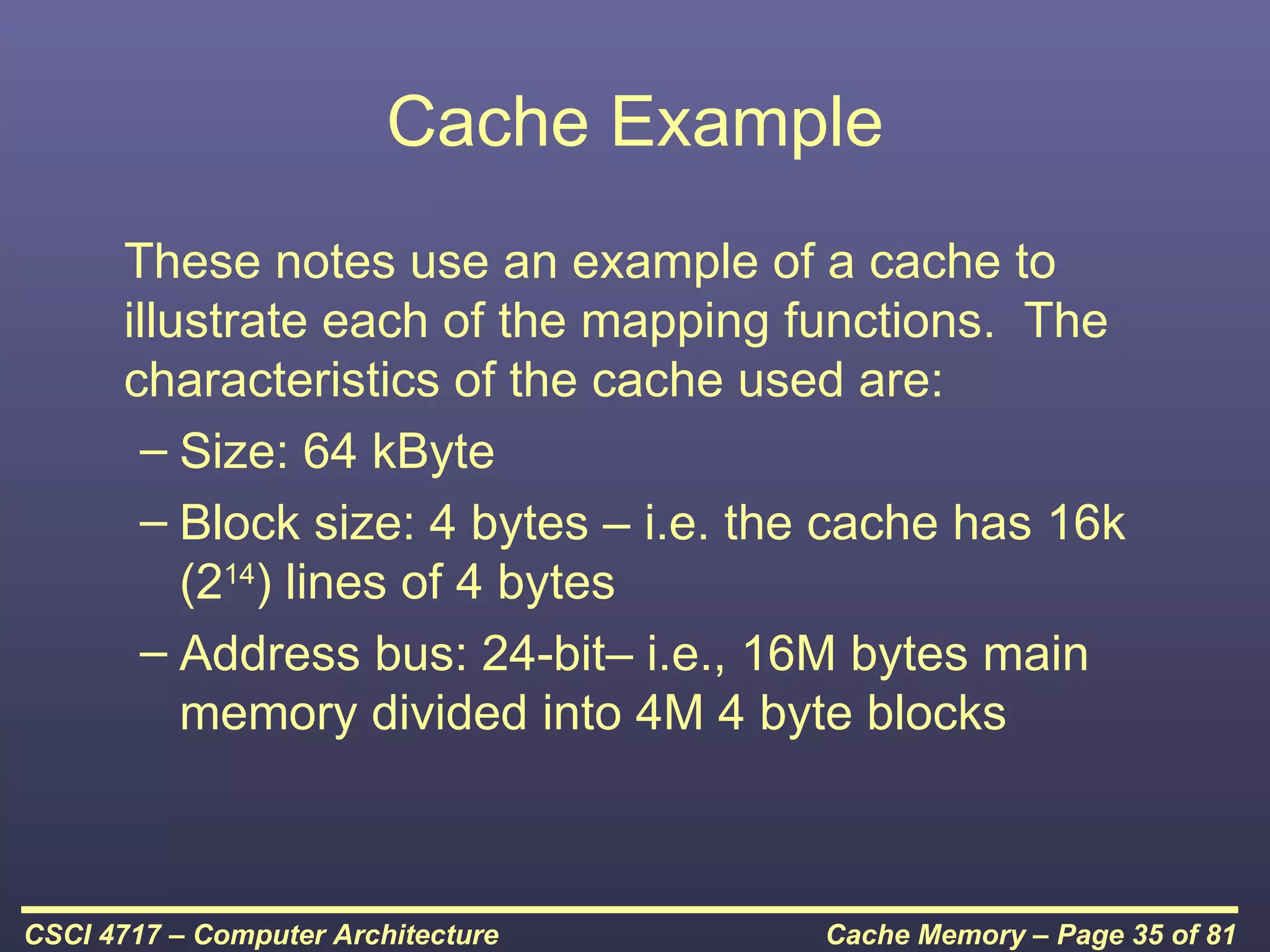
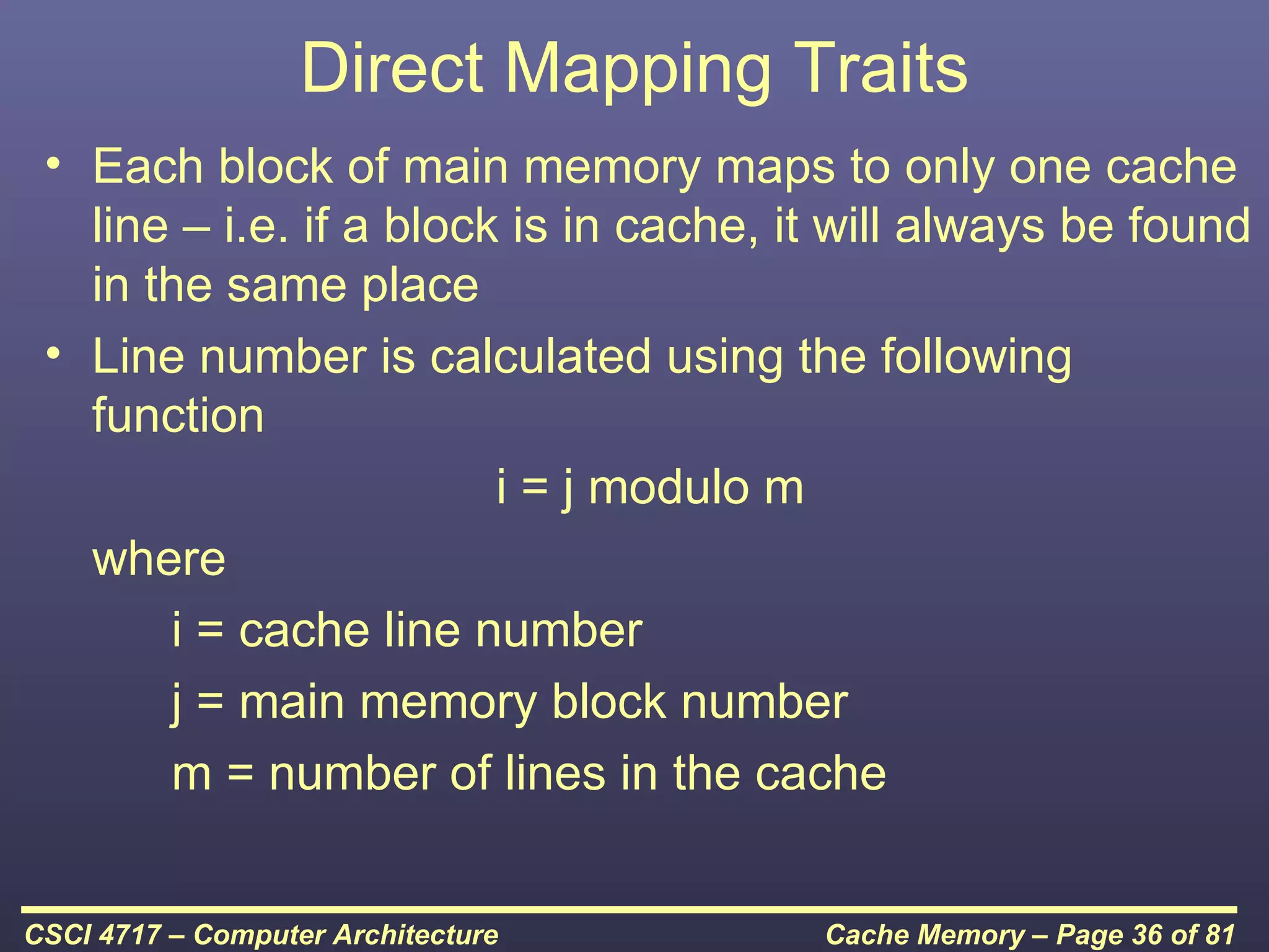
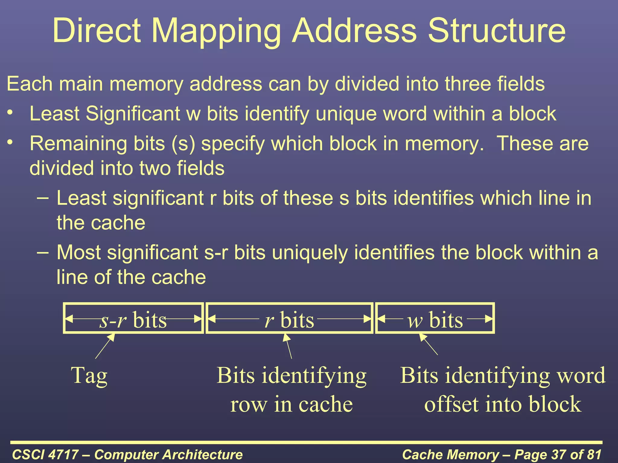
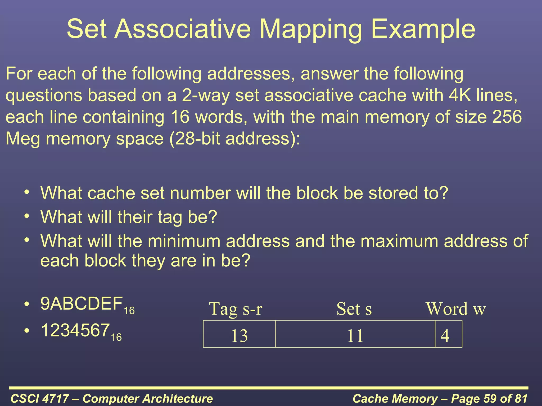
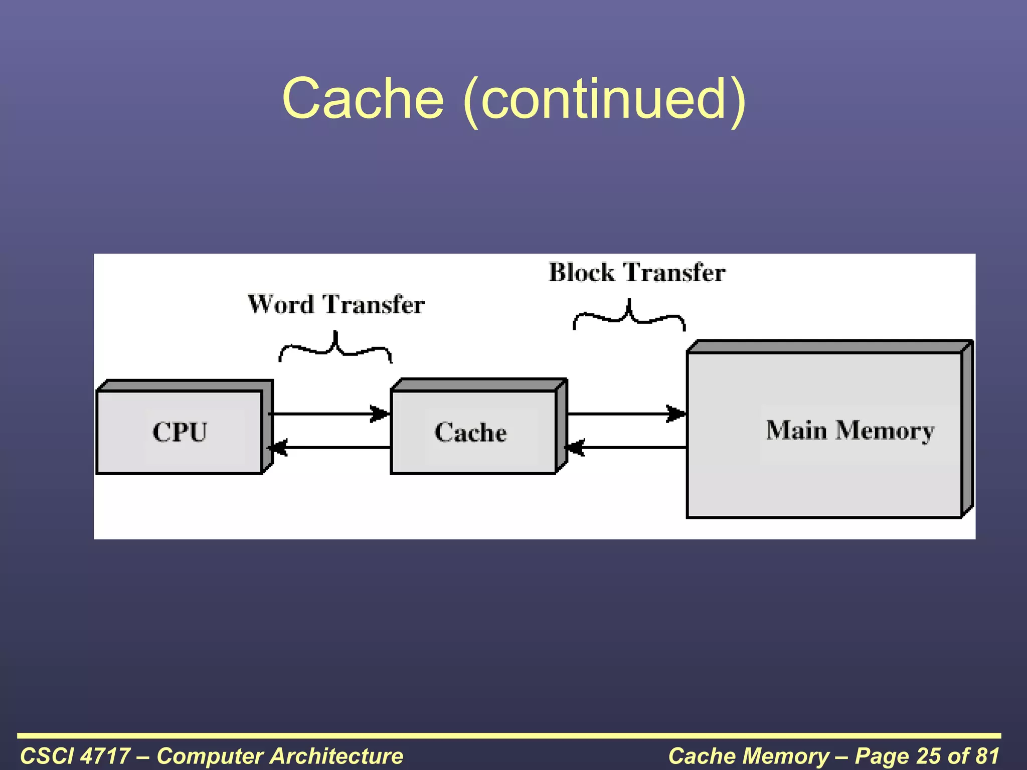
This document discusses cache memory and provides details on its characteristics and operation. It begins by describing the memory hierarchy and how cache fits within it. It then covers the key characteristics of cache memory, including that it is small, fast memory located close to the processor. The document explains how cache works by checking if requested data is present before accessing slower main memory if there is a miss. Overall, the document provides an overview of cache memory fundamentals.
This document discusses Direct Memory Access (DMA). It defines DMA as allowing hardware subsystems like disk drives, graphics cards, and network cards to access system memory independently of the CPU. It describes the principles of DMA in offloading data transfers from the CPU. It also outlines the different DMA operation modes of single transfer, block transfer, and burst block transfer. Uses of DMA include providing high performance I/O and zero copy implementations, while limitations include unpredictable behavior if writing to flash without setting flags.
The document discusses processor organization and architecture. It covers the Von Neumann model, which stores both program instructions and data in the same memory. The Institute for Advanced Study (IAS) computer is described as the first stored-program computer, designed by John von Neumann to overcome limitations of previous computers like the ENIAC. The document also covers the Harvard architecture, instruction formats, register organization including general purpose, address, and status registers, and issues in instruction format design like instruction length and allocation of bits.
Register transfer language & its micro operationsLakshya Sharma
Β
The document discusses register transfer language and micro-operations in digital systems. It describes (1) how register transfer language can be used to describe the sequence of micro-operations involved in any computer function, (2) the four main types of micro-operations - register transfer, arithmetic, logic, and shift micro-operations, giving examples of each, and (3) how register transfers and bus transfers are represented in register transfer language.
The document describes how input/output (I/O) devices communicate with the processor and memory. I/O devices are connected to the processor and memory via a shared bus. Each device has a unique address and uses address, data, and control lines on the bus. Interrupts allow I/O devices to signal the processor when they need attention, reducing wasted processor time. Multiple interrupt lines allow different devices to interrupt independently and ensure the correct interrupt service routine is executed.
The document discusses instruction set architecture (ISA), which is part of computer architecture related to programming. It defines the native data types, instructions, registers, addressing modes, and other low-level aspects of a computer's operation. Well-known ISAs include x86, ARM, MIPS, and RISC. A good ISA lasts through many implementations, supports a variety of uses, and provides convenient functions while permitting efficient implementation. Assembly language is used to program at the level of an ISA's registers, instructions, and execution order.
An instruction code consists of an operation code and operand(s) that specify the operation to perform and data to use. Operation codes are binary codes that define operations like addition, subtraction, etc. Early computers stored programs and data in separate memory sections and used a single accumulator register. Modern computers have multiple registers for temporary storage and performing operations faster than using only memory. Computer instructions encode an operation code and operand fields to specify the basic operations to perform on data stored in registers or memory.
The document discusses different types of instruction codes used in computers. It explains that instruction codes contain operation codes and operands. The operation code specifies the operation to be performed, like addition, subtraction, etc. The operands specify the data on which the operation will be performed, which can be stored in memory or registers. The document outlines three main types of instruction codes - memory reference instructions, register reference instructions, and input-output instructions. It describes the format of each type of instruction and how they are interpreted by the computer.
This document discusses cache memory organization and characteristics. It begins by describing cache location, capacity, unit of transfer, access methods, and physical characteristics. It then covers the different mapping techniques used in caches, including direct mapping, set associative mapping, and fully associative mapping. The document also discusses cache performance factors like hit ratio, replacement algorithms, write policies, block size, and multilevel cache hierarchies. It provides examples of specific processor cache designs like those used in Intel Pentium processors.
General register organization (computer organization)rishi ram khanal
Β
This document discusses the organization of a CPU and its registers. It includes tables that encode the register selection fields and ALU operations. It also provides examples of micro-operations for the CPU, showing the register selections, ALU operations, and control words. Key registers discussed include the accumulator, instruction register, address register, and program counter.
The document discusses instruction execution in a computer processor. It describes how a processor executes instructions by fetching them from memory using the program counter. The instruction is placed in the instruction register and decoded by the control unit. The control unit then selects components like the ALU to carry out operations. Common components involved in instruction execution are the program counter, memory address register, instruction register, memory buffer register, control unit, arithmetic logic unit, and accumulator. The execution cycle involves fetching the instruction from memory address, decoding it, and then executing the instruction.
Bus arbitration is the process of determining which device will become the bus master when multiple devices request access to the bus simultaneously. There are two main types of bus arbitration: centralized arbitration and distributed arbitration. Centralized arbitration uses a single bus controller to manage arbitration, while distributed arbitration allows each device to perform self-arbitration without a central controller. Bus arbitration is needed to avoid conflicts when multiple devices like the CPU and DMA controllers need simultaneous access to the bus. Direct memory access (DMA) allows high-speed transfer of large blocks of data between peripherals and memory without using the CPU.
The document discusses the central processing unit and its components. It describes the general register organization and stack organization of a CPU. It discusses the instruction formats used in CPUs, including three address, two address, one address, zero address, and RISC instruction formats. It also covers addressing modes and data transfer and manipulation instructions used in CPUs.
The 80386 processor architecture is divided into three sections - the central processing unit (CPU), memory management unit (MMU), and bus interface unit (BIU). The CPU contains an execution unit with registers for handling data and calculating offsets, and an instruction unit that decodes instructions. The MMU manages memory using segmentation and paging, dividing physical memory into pages and virtual memory into segments and pages. It provides protection of system code and data. The BUI controls access to the system bus. The 80386 also features eight 32-bit general purpose registers that can be used as 16-bit registers, along with extended 32-bit versions of the BP, SP, SI, and DI registers.
(Ref : Computer System Architecture by Morris Mano 3rd edition) : Microprogrammed Control unit, micro instructions, micro operations, symbolic and binary microprogram.
The document describes the phases of the instruction cycle in a CPU. It discusses the following phases: 1) Fetch - the next instruction is fetched from memory and stored in the instruction register using the program counter; 2) Decode - the instruction inside the register is decoded; 3) Execute - the control unit passes signals to function units like the ALU to perform the required actions like arithmetic or logic operations. It also describes common circuits used in a CPU like the program counter, memory address register, and instruction register.
The document summarizes the key components and functions of the CPU. It describes the CPU's main components like the ALU, control unit, and registers. It explains how the CPU executes instructions in a fetch-decode-execute cycle. It also outlines the three main types of instructions the CPU can execute: arithmetic/logic, memory transfer, and branch instructions. Finally, it provides more details on each step of the instruction execution cycle from fetching the instruction to storing the output.
This document provides an overview of the syllabus for the course CS6303 - Computer Architecture. It covers the following key topics in 3 sentences or less:
- Components of a computer system including input, output, memory, datapath, and control. Instructions and their representation. Addressing modes for accessing operands.
- Eight major ideas in computer architecture: designing for Moore's law, using abstraction, optimizing common cases, performance via parallelism and pipelining, performance via prediction, hierarchy of memories, and dependability via redundancy.
- Evolution from uniprocessors to multiprocessors to address power constraints. Instruction formats, operations, logical and control operations, and different addressing modes for specifying operand locations
The document discusses the arithmetic logic unit (ALU), which is a digital circuit that performs arithmetic and logical operations in a central processing unit (CPU). It first reviews basic CPU concepts like registers and the control unit. It then defines the ALU and describes its typical components and symbol. The remainder of the document demonstrates how to build a simple 1-bit ALU and discusses how multiple 1-bit ALUs can be combined into a larger 32-bit ALU. Useful online resources on ALUs and CPU architecture are also provided.
DMA stands for Direct memory access and is a method of transferring data from the computers RAM to another part of the computer without processing it using theΒ CPU.
There are three main methods to map main memory addresses to cache memory addresses: direct mapping, associative mapping, and set-associative mapping. Direct mapping is the simplest but least flexible method, while associative mapping is most flexible but also slowest. Set-associative mapping combines aspects of the other two methods, dividing the cache into sets with multiple lines to gain efficiency while remaining reasonably flexible.
The document provides an introduction to the 8086 microprocessor. It describes how the 8086 is a 16-bit microprocessor that was launched by Intel in 1978. It discusses the internal architecture of the 8086, including how it employs parallel processing through separate bus interface and execution units to improve performance. It also describes the various registers and memory segmentation used in the 8086 architecture.
The document discusses address sequencing in a microprogram control unit. It begins by defining key terms like control address register, which stores the initial address of the first microinstruction. It then explains that the next address generator is responsible for selecting the next address from control memory based on the current microinstruction. Microinstructions are stored in control memory in groups that make up routines corresponding to each machine instruction. The document also discusses control memory, hardwired control vs microprogrammed control, and examples of next address generation and status bits.
Vector Supercomputers and Scientific Array ProcessorsHsuvas Borkakoty
Β
This presentation discusses vector supercomputers and scientific attached processors. It covers the generations and processing speeds of vector supercomputers, as well as their application areas. Scientific attached processors are designed to enhance the floating point capabilities of host computers and are used to accelerate applications like structural analysis and computational chemistry. The document projects future speeds for scientific attached processors and discusses their advantages of enhancing host machine speeds while having lower costs than mainframes, as well as limitations like requiring microcoding and expensive software.
This document discusses different interconnection structures for multiprocessor systems, including time-shared common bus, multiport memory, crossbar switch, multistage switching network, and hypercube systems. Each structure has advantages and disadvantages related to transfer rate, hardware complexity, and ability to support simultaneous transfers. The hypercube structure connects processors in an n-dimensional cube, allowing messages to route between neighboring nodes that differ in one bit position.
This document discusses the key characteristics of computer memory, including location, capacity, unit of transfer, access methods, performance, physical type, physical characteristics, and organization. It covers different types of memory like CPU registers, main memory, cache, disk, and tape. The different access methods like sequential, direct, random, and associative access are explained. The memory hierarchy and performance aspects like access time, memory cycle time, and transfer rate are defined. Factors like cache size, mapping function, replacement algorithm, write policy, block size that impact cache performance are also summarized.
Cache memory is a small, fast memory located between the CPU and main memory. It stores copies of frequently used instructions and data to accelerate access and improve performance. There are different mapping techniques for cache including direct mapping, associative mapping, and set associative mapping. When the cache is full, replacement algorithms like LRU and FIFO are used to determine which content to remove. The cache can write to main memory using either a write-through or write-back policy.
This document discusses computer architecture and pipelining. It begins with defining the differences between computer organization and architecture. It then outlines the components needed for a MIPS processor implementation including registers, ALU, register file, memory units, and control signals. The document analyzes pipeline hazards such as data, structural, and control hazards. It also evaluates pipeline performance based on clock period, cycles per instruction, and interrupt frequency.
Cache memory is used to improve performance by taking advantage of temporal and spatial locality in memory access patterns. There are typically three main types of cache misses: compulsory misses due to new data, capacity misses when the cache is too small, and conflict misses due to limited cache associativity. Cache design aims to reduce miss rates through greater associativity and larger size, and reduce miss penalties through faster memory and write buffers.
The cache is a small amount of fast memory located close to the CPU that stores frequently accessed and nearby data from main memory in order to speed up data access times for the CPU. Without cache, every data request from the CPU would require accessing the slower main memory. Caches exploit the principle of locality of reference, where programs tend to access the same data repeatedly, to improve performance by fulfilling many requests from the faster cache instead of main memory.
This document discusses cache memory principles and design. It explains that cache memory sits between the CPU and main memory to provide fast access to frequently used data. Cache memory is smaller and faster than main memory. When the CPU requests data, the cache is checked first. If the data is present, it is retrieved from the cache. If not, the block containing the data is copied from main memory into the cache before being sent to the CPU. The cache uses tags to identify which blocks of main memory correspond to each block in the cache.
Cache memory is a type of fast RAM that a computer processor can access more quickly than regular RAM. It stores recently accessed data from main memory to allow for faster future access if the same data is needed again. Cache memory is organized into levels based on proximity and speed of access to the processor, with L1 cache being fastest as it is located directly on the CPU chip, and L2 cache and main memory being progressively slower as they are located further away. Modern processors integrate both L1 and L2 cache onto the CPU package to improve performance by reducing access time.
The document discusses cache memory and provides details about:
1. Cache memory is a small, fast memory located between the CPU and main memory that stores frequently accessed data.
2. There are three main types of cache mapping - direct, associative, and set associative. Direct mapping allows a main memory block to load into only one line in cache. Set associative mapping groups cache lines into sets, with each set containing two or more lines.
3. The document explains cache memory concepts like hits, misses, blocks, lines, tags, and provides examples of different cache mapping techniques.
The document discusses cache organization and mapping techniques. It describes:
1) Direct mapping where each block maps to one line. Set associative mapping divides cache into sets with multiple lines per set.
2) Replacement algorithms like FIFO and LRU that determine which block to replace when the cache is full.
3) Write policies like write-through and write-back that handle writing cached data back to main memory.
Cache memory is a small, fast memory located close to the processor that stores copies of frequently used and recently used data from main memory. When the processor needs to access data, it first checks the cache and if the data is present it can access it quickly from cache. If not present, it loads the data from main memory and stores a copy in cache for faster access next time. There are different types of caches like instruction cache for storing frequently used instructions and data cache for storing frequently used data.
About Cache Memory
working of cache memory
levels of cache memory
mapping techniques for cache memory
1. direct mapping techniques
2. Fully associative mapping techniques
3. set associative mapping techniques
Cache memroy organization
cache coherency
every thing in detail
The document discusses input/output (I/O) interfaces. An I/O interface is required for communication between the CPU, I/O devices, and memory. It performs data buffering, control and timing, and error detection. There are two main techniques for I/O interfacing - memory mapped I/O and I/O mapped I/O. Programmed I/O is an approach where the CPU polls I/O devices by checking their status periodically to see when operations complete.
Cache memory berfungsi mempercepat akses data dengan menyimpan salinan data dari memori utama. Terdapat beberapa elemen rancangan cache seperti ukuran blok, algoritma pengganti, dan fungsi pemetaan yang menentukan lokasi penyimpanan data di cache. Fungsi pemetaan langsung menempatkan setiap blok memori ke baris tunggal cache, sedangkan pemetaan asosiatif memungkinkan blok disimpan pada lokasi manapun.
Cache memory is a small, fast memory located close to the CPU that stores frequently accessed instructions and data. It aims to bridge the gap between the fast CPU and slower main memory. Cache memory is organized into blocks that each contain a tag field identifying the memory address, a data field containing the cached data, and status bits. There are different mapping techniques like direct mapping, associative mapping, and set associative mapping to determine how blocks are stored in cache. When cache is full, replacement algorithms like LRU, FIFO, LFU, and random are used to determine which existing block to replace with the new block.
Virtual memory allows programs to execute without requiring their entire address space to be resident in physical memory. It uses virtual addresses that are translated to physical addresses by the hardware. This translation occurs via page tables managed by the operating system. When a virtual address is accessed, its virtual page number is used as an index into the page table to obtain the corresponding physical page frame number. If the page is not in memory, a page fault occurs and the OS handles loading it from disk. Paging partitions both physical and virtual memory into fixed-sized pages to address fragmentation issues. Segmentation further partitions the virtual address space into logical segments. Hardware support for segmentation involves a segment table containing base/limit pairs for each segment. Translation lookaside buffers
The document summarizes key characteristics of cache memory including location, capacity, unit of transfer, access methods, performance, physical types, organization, and hierarchy. It discusses cache memory in terms of where it is located (internal or external to the CPU), its typical sizes (word, block), access techniques (sequential, random, associative), performance metrics (access time, transfer rate), common physical implementations (SRAM, disk), and organizational aspects like mapping functions, replacement algorithms, and write policies. A cache sits between the CPU and main memory, using fast but small memory to speed up access to frequently used data from larger but slower main memory.
The document discusses various aspects of I/O organization in a computer system. It describes the input-output interface that provides a method for transferring information between internal storage and external I/O devices. It discusses asynchronous data transfer techniques like strobe control and handshaking. It also covers asynchronous serial transmission, different modes of data transfer like programmed I/O, interrupt-initiated I/O, and direct memory access (DMA).
CS304PC:Computer Organization and Architecture Session 29 Memory organization...Asst.prof M.Gokilavani
Β
This document summarizes a session on memory organization that was presented by Asst. Prof. M. Gokilavani at VITS. The session covered topics related to memory hierarchy including main memory, auxiliary memory, associative memory, and cache memory. It described the characteristics of different memory types, such as static vs dynamic RAM, RAM vs ROM, and cache mapping techniques like direct mapping, set-associative mapping, and associative mapping. Examples were provided to illustrate memory addressing and cache organization.
This document summarizes key concepts related to computer memory organization and hierarchy. It discusses how memory is organized from the fastest cache memory up to slower main memory and auxiliary storage. It covers cache mapping techniques like direct mapping, set associative mapping and associative mapping. Virtual memory and paging/segmentation techniques are also summarized. Replacement algorithms for cache memory like FIFO and LRU are discussed. The document provides an overview of computer architecture course topics and assessment patterns.
This document discusses memory management techniques in computer architecture, including:
1) Memory is divided into partitions for the operating system and active processes in a uni-program system, while in a multi-program system memory is further subdivided and shared among active processes.
2) Swapping allows processes to exceed main memory size by storing inactive processes on disk and swapping them back into memory as needed, reducing idle CPU time from I/O waits.
3) Paging maps processes and memory into uniform-sized pages and page frames, using a page table to track mappings and allowing non-contiguous allocation of pages to processes in memory.
This document discusses different techniques for managing memory in computer systems, including uni-program and multi-program memory models, swapping processes in and out of main memory, fixed and variable partitioning of memory, paging through splitting memory and processes into pages, and using page tables to map process pages to memory frames.
Computer architecture refers to the operational design of a computer system. This lecture focuses on the memory subsystem aspects of computer architecture, including memory hierarchy, memory performance, cache organization and operation, random access memory technologies, and bus interfaces. Key topics discussed are memory hierarchy principles like smaller and faster memory levels, cache hit rates, direct mapped, set associative, and write-back caching techniques, and differences between static and dynamic random access memory technologies.
The document discusses computer memory systems and cache memory principles. It provides an overview of:
- The memory hierarchy, which uses different memory technologies arranged in order of decreasing cost per bit, increasing capacity, and increasing access time. This hierarchy satisfies the conflicting demands of large capacity, fast speed, and low cost.
- Cache memory, which sits between the processor and main memory in the hierarchy. Cache memory exploits locality of reference to improve average memory access time.
- Characteristics of different levels of memory, including location, capacity, unit of transfer, access methods, physical types, volatility, and erasability. Faster but smaller and more expensive memories are higher in the hierarchy to satisfy performance needs.
Memory Hierarchy PPT of Computer Organization2022002857mbit
Β
The document discusses memory hierarchy and cache design. It begins by listing sources used to create slides on this topic. It then provides definitions of key terms like cache hit, miss, hit time, and miss penalty. The document explains the principles of memory hierarchy, including exploiting locality of reference and implementing multiple memory levels with decreasing size but increasing speed. It discusses technologies like SRAM and DRAM that are commonly used for caches and main memory. The document also addresses four important questions in cache design: block placement, block identification, block replacement, and write strategy.
Ceph Day Amsterdam 2015: Measuring and predicting performance of Ceph clusters Ceph Community
Β
This document discusses modeling and predicting performance in Ceph distributed storage systems. It provides an overview of Ceph, including its object storage, block storage, and file system capabilities. It then discusses various factors that impact Ceph performance, such as network configuration, storage node hardware, number of disks, caching, redundancy settings, and placement groups. The document notes there are many configuration choices and tradeoffs to consider when designing a Ceph cluster to meet performance requirements.
The document discusses computer memory hierarchy and cache organization. It begins by outlining the memory pyramid from fastest and smallest registers to largest but slowest hard disks. It then discusses cache organization including direct mapped, set associative and fully associative caches. The key points are:
Caches aim to bridge the speed gap between fast processors and slow main memory. Caches exploit temporal and spatial locality to reduce average memory access time. Caches are organized into blocks and sets to store recently accessed data from main memory.
1. The document discusses memory management and the memory hierarchy in computer systems. It describes the different levels of memory including CPU registers, main memory, cache memory, and auxiliary memory.
2. Cache memory is used to reduce the average time required to access memory by taking advantage of spatial and temporal locality. There are three common cache mapping techniques - direct mapping, associative mapping, and set-associative mapping.
3. Virtual memory allows programs to behave as if they have a large, single memory space even if physical memory is smaller. It uses a memory management unit to translate virtual addresses to physical addresses through a page table.
MT48 A Flash into the future of storageβ¦.Β Flash meets Persistent Memory: The...Dell EMC World
Β
Several key technology trends are redefining the boundaries of the traditional storage infrastructure stack:Β In a rapidly changing world of system interconnects, emerging memory media, and storage semantics, Server Designers and Storage Architects are engaging and collaborating like never before to exploit breakthrough technology capabilities.
With the backdrop of Big Data volume, Cloud Data ubiquity and IoT Data velocity, Application Developers are entering the Post-POSIX world of real-time, high-frequency, low latency data management frameworks.Β Β
This session will address key technology trends in Storage, Networking, and Compute, as they define the parameters of a Memory Centric Architecture (MCA) and the Next Generation Data Center.
This document discusses various concepts related to computer memory. It defines key terminology like capacity, word size, and access time. It describes different types of memory technologies like RAM, ROM, SRAM and DRAM. It also discusses memory hierarchy concepts like cache organization, cache performance, and cache optimization techniques. Finally, it provides an overview of external storage technologies like RAID levels 0, 1, 5 and 10.
This document provides an introduction to computer hardware. It discusses what a computer is and its basic components like input, output, processing and storage devices. It explains the differences between various types of computer memory like RAM, ROM, cache and primary memory. It also discusses concepts like Moore's Law and how computer performance and memory capacity have increased exponentially over time.
1. The basic components of a parallel computer are processors, memory, and an interconnect network that connects the processors and memory.
2. Key processor terms include RISC, pipelining, and superscalar, which refer to instruction processing techniques. The network interconnect is characterized by latency, bandwidth, and topology.
3. Memory terms include cache, which sits between the CPU and main memory, as well as instruction cache, data cache, secondary cache, and translation lookaside buffer. Caches provide faster access to frequently used data and instructions.
When dealing with infrastructure we often go through the process of determining the different resources needed to attend our application requirements. This talks looks into the way that resources are used by MongoDB and which aspects should be considered to determined the sizing, capacity and deployment of a MongoDB cluster given the different scenarios, different sets of operations and storage engines available.
The document discusses various topics related to memory management in operating systems including swapping, contiguous memory allocation, paging, segmentation, virtual memory concepts like demand paging, page replacement, and thrashing. It provides details on page tables, segmentation hardware, logical to physical address translation, and performance aspects of demand paging. The key aspects covered are memory management techniques to overcome fragmentation and enable efficient use of limited main memory.
The document discusses the history and evolution of computer hardware from the first generation of vacuum tube computers to current generation computers using grand-scale integrated circuits. It describes the main components of computer hardware including the central processing unit, primary and secondary storage, and input/output devices. It also covers topics such as computer memory, microprocessors, and emerging technologies.
This document discusses multiprocessors and multiprocessing. It covers topics such as why you would want a multiprocessor, cache coherence issues that arise in shared memory multiprocessors, and different approaches to cache coherence like snoopy protocols and directory-based schemes. It also discusses classification of multiprocessors based on factors like the Flynn taxonomy, interconnection network, memory topology, and programming model.
Cache memory is a small, fast memory located close to the CPU that stores frequently accessed data from main memory to speed up processing. It is organized into multiple levels - L1 cache is inside the CPU, L2 cache is external, and main memory is L3. The cache improves performance by reducing access time - when data is in cache it is a "hit" and very fast to access, while a "miss" requires loading from main memory which is slower. Factors like cache size, mapping technique, replacement policy, and write strategy impact how efficiently it services memory requests.
Dandelion Hashtable: beyond billion requests per second on a commodity serverAntonios Katsarakis
Β
This slide deck presents DLHT, a concurrent in-memory hashtable. Despite efforts to optimize hashtables, that go as far as sacrificing core functionality, state-of-the-art designs still incur multiple memory accesses per request and block request processing in three cases. First, most hashtables block while waiting for data to be retrieved from memory. Second, open-addressing designs, which represent the current state-of-the-art, either cannot free index slots on deletes or must block all requests to do so. Third, index resizes block every request until all objects are copied to the new index. Defying folklore wisdom, DLHT forgoes open-addressing and adopts a fully-featured and memory-aware closed-addressing design based on bounded cache-line-chaining. This design offers lock-free index operations and deletes that free slots instantly, (2) completes most requests with a single memory access, (3) utilizes software prefetching to hide memory latencies, and (4) employs a novel non-blocking and parallel resizing. In a commodity server and a memory-resident workload, DLHT surpasses 1.6B requests per second and provides 3.5x (12x) the throughput of the state-of-the-art closed-addressing (open-addressing) resizable hashtable on Gets (Deletes).
[OReilly Superstream] Occupy the Space: A grassroots guide to engineering (an...Jason Yip
Β
The typical problem in product engineering is not bad strategy, so much as βno strategyβ. This leads to confusion, lack of motivation, and incoherent action. The next time you look for a strategy and find an empty space, instead of waiting for it to be filled, I will show you how to fill it in yourself. If youβre wrong, it forces a correction. If youβre right, it helps create focus. Iβll share how Iβve approached this in the past, both what works and lessons for what didnβt work so well.
Must Know Postgres Extension for DBA and Developer during MigrationMydbops
Β
Mydbops Opensource Database Meetup 16
Topic: Must-Know PostgreSQL Extensions for Developers and DBAs During Migration
Speaker: Deepak Mahto, Founder of DataCloudGaze Consulting
Date & Time: 8th June | 10 AM - 1 PM IST
Venue: Bangalore International Centre, Bangalore
Abstract: Discover how PostgreSQL extensions can be your secret weapon! This talk explores how key extensions enhance database capabilities and streamline the migration process for users moving from other relational databases like Oracle.
Key Takeaways:
* Learn about crucial extensions like oracle_fdw, pgtt, and pg_audit that ease migration complexities.
* Gain valuable strategies for implementing these extensions in PostgreSQL to achieve license freedom.
* Discover how these key extensions can empower both developers and DBAs during the migration process.
* Don't miss this chance to gain practical knowledge from an industry expert and stay updated on the latest open-source database trends.
Mydbops Managed Services specializes in taking the pain out of database management while optimizing performance. Since 2015, we have been providing top-notch support and assistance for the top three open-source databases: MySQL, MongoDB, and PostgreSQL.
Our team offers a wide range of services, including assistance, support, consulting, 24/7 operations, and expertise in all relevant technologies. We help organizations improve their database's performance, scalability, efficiency, and availability.
Contact us: info@mydbops.com
Visit: https://www.mydbops.com/
Follow us on LinkedIn: https://in.linkedin.com/company/mydbops
For more details and updates, please follow up the below links.
Meetup Page : https://www.meetup.com/mydbops-databa...
ββTwitter: https://twitter.com/mydbopsofficial
Blogs: https://www.mydbops.com/blog/
β
βFacebook(Meta): https://www.facebook.com/mydbops/
The Microsoft 365 Migration Tutorial For Beginner.pptxoperationspcvita
Β
This presentation will help you understand the power of Microsoft 365. However, we have mentioned every productivity app included in Office 365. Additionally, we have suggested the migration situation related to Office 365 and how we can help you.
You can also read: https://www.systoolsgroup.com/updates/office-365-tenant-to-tenant-migration-step-by-step-complete-guide/
High performance Serverless Java on AWS- GoTo Amsterdam 2024Vadym Kazulkin
Β
Java is for many years one of the most popular programming languages, but it used to have hard times in the Serverless community. Java is known for its high cold start times and high memory footprint, comparing to other programming languages like Node.js and Python. In this talk I'll look at the general best practices and techniques we can use to decrease memory consumption, cold start times for Java Serverless development on AWS including GraalVM (Native Image) and AWS own offering SnapStart based on Firecracker microVM snapshot and restore and CRaC (Coordinated Restore at Checkpoint) runtime hooks. I'll also provide a lot of benchmarking on Lambda functions trying out various deployment package sizes, Lambda memory settings, Java compilation options and HTTP (a)synchronous clients and measure their impact on cold and warm start times.
This talk will cover ScyllaDB Architecture from the cluster-level view and zoom in on data distribution and internal node architecture. In the process, we will learn the secret sauce used to get ScyllaDB's high availability and superior performance. We will also touch on the upcoming changes to ScyllaDB architecture, moving to strongly consistent metadata and tablets.
"Frontline Battles with DDoS: Best practices and Lessons Learned", Igor IvaniukFwdays
Β
At this talk we will discuss DDoS protection tools and best practices, discuss network architectures and what AWS has to offer. Also, we will look into one of the largest DDoS attacks on Ukrainian infrastructure that happened in February 2022. We'll see, what techniques helped to keep the web resources available for Ukrainians and how AWS improved DDoS protection for all customers based on Ukraine experience
Taking AI to the Next Level in Manufacturing.pdfssuserfac0301
Β
Read Taking AI to the Next Level in Manufacturing to gain insights on AI adoption in the manufacturing industry, such as:
1. How quickly AI is being implemented in manufacturing.
2. Which barriers stand in the way of AI adoption.
3. How data quality and governance form the backbone of AI.
4. Organizational processes and structures that may inhibit effective AI adoption.
6. Ideas and approaches to help build your organization's AI strategy.
Monitoring and Managing Anomaly Detection on OpenShift.pdfTosin Akinosho
Β
Monitoring and Managing Anomaly Detection on OpenShift
Overview
Dive into the world of anomaly detection on edge devices with our comprehensive hands-on tutorial. This SlideShare presentation will guide you through the entire process, from data collection and model training to edge deployment and real-time monitoring. Perfect for those looking to implement robust anomaly detection systems on resource-constrained IoT/edge devices.
Key Topics Covered
1. Introduction to Anomaly Detection
- Understand the fundamentals of anomaly detection and its importance in identifying unusual behavior or failures in systems.
2. Understanding Edge (IoT)
- Learn about edge computing and IoT, and how they enable real-time data processing and decision-making at the source.
3. What is ArgoCD?
- Discover ArgoCD, a declarative, GitOps continuous delivery tool for Kubernetes, and its role in deploying applications on edge devices.
4. Deployment Using ArgoCD for Edge Devices
- Step-by-step guide on deploying anomaly detection models on edge devices using ArgoCD.
5. Introduction to Apache Kafka and S3
- Explore Apache Kafka for real-time data streaming and Amazon S3 for scalable storage solutions.
6. Viewing Kafka Messages in the Data Lake
- Learn how to view and analyze Kafka messages stored in a data lake for better insights.
7. What is Prometheus?
- Get to know Prometheus, an open-source monitoring and alerting toolkit, and its application in monitoring edge devices.
8. Monitoring Application Metrics with Prometheus
- Detailed instructions on setting up Prometheus to monitor the performance and health of your anomaly detection system.
9. What is Camel K?
- Introduction to Camel K, a lightweight integration framework built on Apache Camel, designed for Kubernetes.
10. Configuring Camel K Integrations for Data Pipelines
- Learn how to configure Camel K for seamless data pipeline integrations in your anomaly detection workflow.
11. What is a Jupyter Notebook?
- Overview of Jupyter Notebooks, an open-source web application for creating and sharing documents with live code, equations, visualizations, and narrative text.
12. Jupyter Notebooks with Code Examples
- Hands-on examples and code snippets in Jupyter Notebooks to help you implement and test anomaly detection models.
Have you ever been confused by the myriad of choices offered by AWS for hosting a website or an API?
Lambda, Elastic Beanstalk, Lightsail, Amplify, S3 (and more!) can each host websites + APIs. But which one should we choose?
Which one is cheapest? Which one is fastest? Which one will scale to meet our needs?
Join me in this session as we dive into each AWS hosting service to determine which one is best for your scenario and explain why!
Main news related to the CCS TSI 2023 (2023/1695)Jakub Marek
Β
An English π¬π§ translation of a presentation to the speech I gave about the main changes brought by CCS TSI 2023 at the biggest Czech conference on Communications and signalling systems on Railways, which was held in Clarion Hotel Olomouc from 7th to 9th November 2023 (konferenceszt.cz). Attended by around 500 participants and 200 on-line followers.
The original Czech π¨πΏ version of the presentation can be found here: https://www.slideshare.net/slideshow/hlavni-novinky-souvisejici-s-ccs-tsi-2023-2023-1695/269688092 .
The videorecording (in Czech) from the presentation is available here: https://youtu.be/WzjJWm4IyPk?si=SImb06tuXGb30BEH .
Essentials of Automations: Exploring Attributes & Automation ParametersSafe Software
Β
Building automations in FME Flow can save time, money, and help businesses scale by eliminating data silos and providing data to stakeholders in real-time. One essential component to orchestrating complex automations is the use of attributes & automation parameters (both formerly known as βkeysβ). In fact, itβs unlikely youβll ever build an Automation without using these components, but what exactly are they?
Attributes & automation parameters enable the automation author to pass data values from one automation component to the next. During this webinar, our FME Flow Specialists will cover leveraging the three types of these output attributes & parameters in FME Flow: Event, Custom, and Automation. As a bonus, theyβll also be making use of the Split-Merge Block functionality.
Youβll leave this webinar with a better understanding of how to maximize the potential of automations by making use of attributes & automation parameters, with the ultimate goal of setting your enterprise integration workflows up on autopilot.
Connector Corner: Seamlessly power UiPath Apps, GenAI with prebuilt connectorsDianaGray10
Β
Join us to learn how UiPath Apps can directly and easily interact with prebuilt connectors via Integration Service--including Salesforce, ServiceNow, Open GenAI, and more.
The best part is you can achieve this without building a custom workflow! Say goodbye to the hassle of using separate automations to call APIs. By seamlessly integrating within App Studio, you can now easily streamline your workflow, while gaining direct access to our Connector Catalog of popular applications.
Weβll discuss and demo the benefits of UiPath Apps and connectors including:
Creating a compelling user experience for any software, without the limitations of APIs.
Accelerating the app creation process, saving time and effort
Enjoying high-performance CRUD (create, read, update, delete) operations, for
seamless data management.
Speakers:
Russell Alfeche, Technology Leader, RPA at qBotic and UiPath MVP
Charlie Greenberg, host
2. Characteristics of Memory
βLocation wrt Processorβ
β’ Inside CPU β temporary memory or
registers
β’ Inside processor β L1 cache
β’ Motherboard β main memory and L2
cache
β’ Main memory β DRAM and L3 cache
β’ External β peripherals such as disk, tape,
and networked memory devices
CSCI 4717 β Computer Architecture Cache Memory β Page 2 of 81
3. Characteristics of Memory
βCapacity β Word Sizeβ
β’ The natural data size for a processor.
β’ A 32-bit processor has a 32-bit word.
β’ Typically based on processor's data bus
width (i.e., the width of an integer or an
instruction)
β’ Varying widths can be obtained by putting
memory chips in parallel with same
address lines
CSCI 4717 β Computer Architecture Cache Memory β Page 3 of 81
4. Characteristics of Memory
βCapacity β Addressable Unitsβ
β’ Varies based on the system's ability to
allow addressing at byte level etc.
β’ Typically smallest location which can be
uniquely addressed
β’ At mother board level, this is the word
β’ It is a cluster on disks
β’ Addressable units (N) equals 2 raised to
the power of the number of bits in the
address bus
CSCI 4717 β Computer Architecture Cache Memory β Page 4 of 81
5. Characteristics of Memory
βUnit of transferβ
β’ The number of bits read out of or written
into memory at a time.
β’ Internal β Usually governed by data bus
width, i.e., a word
β’ External β Usually a block which is much
larger than a word
CSCI 4717 β Computer Architecture Cache Memory β Page 5 of 81
6. Characteristics of Memory
βAccess methodβ
β’ Based on the hardware implementation of
the storage device
β’ Four types
β Sequential
β Direct
β Random
β Associative
CSCI 4717 β Computer Architecture Cache Memory β Page 6 of 81
7. Sequential Access Method
β’ Start at the beginning and read through in
order
β’ Access time depends on location of data
and previous location
β’ Example: tape
CSCI 4717 β Computer Architecture Cache Memory β Page 7 of 81
8. Direct Access Method
β’ Individual blocks have unique address
β’ Access is by jumping to vicinity then
performing a sequential search
β’ Access time depends on location of data
within "block" and previous location
β’ Example: hard disk
CSCI 4717 β Computer Architecture Cache Memory β Page 8 of 81
9. Random Access Method
β’ Individual addresses identify locations
exactly
β’ Access time is consistent across all
locations and is independent previous
access
β’ Example: RAM
CSCI 4717 β Computer Architecture Cache Memory β Page 9 of 81
10. Associative Access Method
β’ Addressing information must be stored
with data in a general data location
β’ A specific data element is located by a
comparing desired address with address
portion of stored elements
β’ Access time is independent of location or
previous access
β’ Example: cache
CSCI 4717 β Computer Architecture Cache Memory β Page 10 of 81
11. Performance β Access Time
β’ Time between "requesting" data and getting it
β’ RAM
β Time between putting address on bus and getting
data.
β It's predictable.
β’ Other types, Sequential, Direct, Associative
β Time it takes to position the read-write mechanism at
the desired location.
β Not predictable.
CSCI 4717 β Computer Architecture Cache Memory β Page 11 of 81
12. Performance β Memory Cycle time
β’ Primarily a RAM phenomenon
β’ Adds "recovery" time to cycle allowing for
transients to dissipate so that next access is
reliable.
β’ Cycle time is access + recovery
CSCI 4717 β Computer Architecture Cache Memory β Page 12 of 81
13. Performance β Transfer Rate
β’ Rate at which data can be moved
β’ RAM β Predictable; equals 1/(cycle time)
β’ Non-RAM β Not predictable; equals
TN = TA + (N/R)
where
β TN = Average time to read or write N bits
β TA = Average access time
β N = Number of bits
β R = Transfer rate in bits per second
CSCI 4717 β Computer Architecture Cache Memory β Page 13 of 81
14. Physical Types
β’ Semiconductor β RAM
β’ Magnetic β Disk & Tape
β’ Optical β CD & DVD
β’ Others
β Bubble (old) β memory that made a "bubble" of
charge in an opposite direction to that of the thin
magnetic material that on which it was mounted
β Hologram (new) β much like the hologram on your
credit card, laser beams are used to store computer-
generated data in three dimensions. (10 times faster
with 12 times the density)
CSCI 4717 β Computer Architecture Cache Memory β Page 14 of 81
15. Physical Characteristics
β’ Decay
β Power loss
β Degradation over time
β’ Volatility β RAM vs. Flash
β’ Erasable β RAM vs. ROM
β’ Power consumption β More specific to laptops,
PDAs, and embedded systems
CSCI 4717 β Computer Architecture Cache Memory β Page 15 of 81
16. Organization
β’ Physical arrangement of bits into words
β’ Not always obvious
β’ Non-sequential arrangements may be due to
speed or reliability benefits, e.g. interleaved
CSCI 4717 β Computer Architecture Cache Memory β Page 16 of 81
17. Memory Hierarchy
β’ Trade-offs among three key characteristics
β Amount β Software will ALWAYS fill available
memory
β Speed β Memory should be able to keep up with
the processor
β Cost β Whatever the market will bear
β’ Balance these three characteristics with a memory
hierarchy
β’ Analogy β
Refrigerator & cupboard (fast access β lowest
variety)
freezer & pantry (slower access β better variety)
grocery store (slowest access β greatest variety)
CSCI 4717 β Computer Architecture Cache Memory β Page 17 of 81
18. Memory Hierarch (continued)
Implementation β Going down the
hierarchy has the following results:
β Decreasing cost per bit (cheaper)
β Increasing capacity (larger)
β Increasing access time (slower)
β KEY β Decreasing frequency of access of the
memory by the processor
CSCI 4717 β Computer Architecture Cache Memory β Page 18 of 81
19. Memory Hierarch (continued)
Source: Null, Linda and Lobur, Julia (2003). Computer Organization
and Architecture (p. 236). Sudbury, MA: Jones and Bartlett Publishers.
CSCI 4717 β Computer Architecture Cache Memory β Page 19 of 81
20. Mechanics of Technology
β’ The basic mechanics of creating memory
directly affect the first three characteristics
of the hierarchy:
β Decreasing cost per bit
β Increasing capacity
β Increasing access time
β’ The fourth characteristic is met because of
a principle known as locality of reference
CSCI 4717 β Computer Architecture Cache Memory β Page 20 of 81
21. Locality of Reference
Due to the nature of programming,
instructions and data tend to cluster
together (loops, subroutines, and data
structures)
β Over a long period of time, clusters will
change
β Over a short period, clusters will tend to be
the same
CSCI 4717 β Computer Architecture Cache Memory β Page 21 of 81
22. Breaking Memory into Levels
β’ Assume a hypothetical system has two levels of
memory
β Level 2 should contain all instructions and data
β Level 1 doesn't have room for everything, so when
a new cluster is required, the cluster it replaces
must be sent back to the level 2
β’ These principles can be applied to much more than
just two levels
β’ If performance is based on amount of memory rather
than speed, lower levels can be used to simulate
larger sizes for higher levels, e.g., virtual memory
CSCI 4717 β Computer Architecture Cache Memory β Page 22 of 81
24. Cache
β’ What is it? A cache is a small amount of fast
memory
β’ What makes small fast?
β Simpler decoding logic
β More expensive SRAM technology
β Close proximity to processor β Cache sits
between normal main memory and CPU or it
may be located on CPU chip or module
CSCI 4717 β Computer Architecture Cache Memory β Page 24 of 81
26. Cache operation β overview
β’ CPU requests contents of memory location
β’ Check cache for this data
β’ If present, get from cache (fast)
β’ If not present, one of two things happens:
β read required block from main memory to cache
then deliver from cache to CPU (cache physically
between CPU and bus)
β read required block from main memory to cache
and simultaneously deliver to CPU (CPU and
cache both receive data from the same data bus
buffer)
CSCI 4717 β Computer Architecture Cache Memory β Page 26 of 81
27. Going Deeper with Principle of Locality
β’ Cache "misses" are unavoidable, i.e., every piece of
data and code thing must be loaded at least once
β’ What does a processor do during a miss? It waits for
the data to be loaded.
β’ Power consumption varies linearly with clock speed
and the square of the voltage.
CSCI 4717 β Computer Architecture Cache Memory β Page 27 of 81
28. Cache Structure
β’ Cache includes tags to identify the address of
the block of main memory contained in a line
of the cache
β’ Each word in main memory has a unique n-bit
address
β’ There are M=2n/K block of K words in main
memory
β’ Cache contains C lines of K words each plus
a tag uniquely identifying the block of K words
CSCI 4717 β Computer Architecture Cache Memory β Page 28 of 81
29. Cache Structure (continued)
Line
number Tag Block
0
1
2
C-1
Block length
(K words)
CSCI 4717 β Computer Architecture Cache Memory β Page 29 of 81
30. Memory Divided into Blocks
Memory
Address
1
2
3 Block of
K words
Block
2n-1
Word length
CSCI 4717 β Computer Architecture Cache Memory β Page 30 of 81
31. Cache Design
β’ Size
β’ Mapping Function
β’ Replacement Algorithm
β’ Write Policy
β’ Block Size
β’ Number of Caches
CSCI 4717 β Computer Architecture Cache Memory β Page 31 of 81
32. Cache size
β’ Cost β More cache is expensive
β’ Speed
β More cache is faster (up to a point)
β Larger decoding circuits slow up a cache
β Algorithm is needed for mapping main
memory addresses to lines in the cache. This
takes more time than just a direct RAM
CSCI 4717 β Computer Architecture Cache Memory β Page 32 of 81
34. Mapping Functions
β’ A mapping function is the method used to locate
a memory address within a cache
β’ It is used when copying a block from main
memory to the cache and it is used again when
trying to retrieve data from the cache
β’ There are three kinds of mapping functions
β Direct
β Associative
β Set Associative
CSCI 4717 β Computer Architecture Cache Memory β Page 34 of 81
35. Cache Example
These notes use an example of a cache to
illustrate each of the mapping functions. The
characteristics of the cache used are:
β Size: 64 kByte
β Block size: 4 bytes β i.e. the cache has 16k
(214) lines of 4 bytes
β Address bus: 24-bitβ i.e., 16M bytes main
memory divided into 4M 4 byte blocks
CSCI 4717 β Computer Architecture Cache Memory β Page 35 of 81
36. Direct Mapping Traits
β’ Each block of main memory maps to only one cache
line β i.e. if a block is in cache, it will always be found
in the same place
β’ Line number is calculated using the following
function
i = j modulo m
where
i = cache line number
j = main memory block number
m = number of lines in the cache
CSCI 4717 β Computer Architecture Cache Memory β Page 36 of 81
37. Direct Mapping Address Structure
Each main memory address can by divided into three fields
β’ Least Significant w bits identify unique word within a block
β’ Remaining bits (s) specify which block in memory. These are
divided into two fields
β Least significant r bits of these s bits identifies which line in
the cache
β Most significant s-r bits uniquely identifies the block within a
line of the cache
s-r bits r bits w bits
Tag Bits identifying Bits identifying word
row in cache offset into block
CSCI 4717 β Computer Architecture Cache Memory β Page 37 of 81
38. Direct Mapping Address Structure
(continued)
β’ Why are the r-bits used to identify which
line in cache?
β’ More likely to have unique r bits than s-r
bits based on principle of locality of
reference
CSCI 4717 β Computer Architecture Cache Memory β Page 38 of 81
39. Direct Mapping Address Structure Example
Tag s-r Line or slot r Word w
8 14 2
β’ 24 bit address
β’ 2 bit word identifier (4 byte block)
β’ 22 bit block identifier
β’ 8 bit tag (=22β14)
β’ 14 bit slot or line
β’ No two blocks in the same line have the same tag
β’ Check contents of cache by finding line and
comparing tag
CSCI 4717 β Computer Architecture Cache Memory β Page 39 of 81
40. Direct Mapping Cache Line Table
Cache line Main Memory blocks held
0 0, m, 2m, 3mβ¦2sβm
1 1, m+1, 2m+1β¦2sβm+1
mβ1 mβ1, 2mβ1, 3mβ1β¦2sβ1
CSCI 4717 β Computer Architecture Cache Memory β Page 40 of 81
41. Direct Mapping Cache Organization
CSCI 4717 β Computer Architecture Cache Memory β Page 41 of 81
43. Direct Mapping Examples
What cache line number will the following
addresses be stored to, and what will the
minimum address and the maximum address of
each block they are in be if we have a cache
with 4K lines of 16 words to a block in a 256
Meg memory space (28-bit address)?
Tag s-r Line or slot r Word w
12 12 4
a.) 9ABCDEF16
b.) 123456716
CSCI 4717 β Computer Architecture Cache Memory β Page 43 of 81
44. More Direct Mapping Examples
Assume that a portion of the tags in the cache in our example
looks like the table below. Which of the following addresses are
contained in the cache?
a.) 438EE816 b.) F18EFF16 c.) 6B8EF316 d.) AD8EF316
Tag (binary) Line number (binary) Addresses wi/ block
00 01 10 11
0100 0011 1000 1110 1110 10
1110 1101 1000 1110 1110 11
1010 1101 1000 1110 1111 00
0110 1011 1000 1110 1111 00
1011 0101 1000 1110 1111 10
1111 0001 1000 1110 1111 11
CSCI 4717 β Computer Architecture Cache Memory β Page 44 of 81
45. Direct Mapping Summary
β’ Address length = (s + w) bits
β’ Number of addressable units = 2s+w words or
bytes
β’ Block size = line width = 2w words or bytes
β’ Number of blocks in main memory = 2s+ w/2w = 2s
β’ Number of lines in cache = m = 2r
β’ Size of tag = (s β r) bits
CSCI 4717 β Computer Architecture Cache Memory β Page 45 of 81
46. Direct Mapping pros & cons
β’ Simple
β’ Inexpensive
β’ Fixed location for given block β
If a program accesses 2 blocks that map to the
same line repeatedly, cache misses are very
high (thrashing)
CSCI 4717 β Computer Architecture Cache Memory β Page 46 of 81
47. Associative Mapping Traits
β’ A main memory block can load into any line of
cache
β’ Memory address is interpreted as:
β Least significant w bits = word position within block
β Most significant s bits = tag used to identify which
block is stored in a particular line of cache
β’ Every line's tag must be examined for a match
β’ Cache searching gets expensive and slower
CSCI 4717 β Computer Architecture Cache Memory β Page 47 of 81
48. Associative Mapping Address Structure
Example
Tag β s bits Word β w bits
(22 in example) (2 in ex.)
β’ 22 bit tag stored with each 32 bit block of data
β’ Compare tag field with tag entry in cache to
check for hit
β’ Least significant 2 bits of address identify which
of the four 8 bit words is required from 32 bit
data block
CSCI 4717 β Computer Architecture Cache Memory β Page 48 of 81
51. Fully Associative Mapping Example
Assume that a portion of the tags in the cache in our example
looks like the table below. Which of the following addresses are
contained in the cache?
a.) 438EE816 b.) F18EFF16 c.) 6B8EF316 d.) AD8EF316
Tag (binary) Addresses wi/ block
00 01 10 11
0100 0011 1000 1110 1110 10
1110 1101 1100 1001 1011 01
1010 1101 1000 1110 1111 00
0110 1011 1000 1110 1111 00
1011 0101 0101 1001 0010 00
1111 0001 1000 1110 1111 11
CSCI 4717 β Computer Architecture Cache Memory β Page 51 of 81
52. Associative Mapping Summary
β’ Address length = (s + w) bits
β’ Number of addressable units = 2s+w words or
bytes
β’ Block size = line size = 2w words or bytes
β’ Number of blocks in main memory = 2s+ w/2w = 2s
β’ Number of lines in cache = undetermined
β’ Size of tag = s bits
CSCI 4717 β Computer Architecture Cache Memory β Page 52 of 81
53. Set Associative Mapping Traits
β’ Address length is s + w bits
β’ Cache is divided into a number of sets, v = 2d
β’ k blocks/lines can be contained within each set
β’ k lines in a cache is called a k-way set
associative mapping
β’ Number of lines in a cache = vβ’k = kβ’2d
β’ Size of tag = (s-d) bits
CSCI 4717 β Computer Architecture Cache Memory β Page 53 of 81
54. Set Associative Mapping Traits (continued)
β’ Hybrid of Direct and Associative
k = 1, this is basically direct mapping
v = 1, this is associative mapping
β’ Each set contains a number of lines, basically the number of
lines divided by the number of sets
β’ A given block maps to any line within its specified set β e.g.
Block B can be in any line of set i.
β’ 2 lines per set is the most common organization.
β Called 2 way associative mapping
β A given block can be in one of 2 lines in only one specific
set
β Significant improvement over direct mapping
CSCI 4717 β Computer Architecture Cache Memory β Page 54 of 81
55. K-Way Set Associative Cache Organization
CSCI 4717 β Computer Architecture Cache Memory β Page 55 of 81
56. How does this affect our example?
β’ Letβs go to two-way set associative mapping
β’ Divides the 16K lines into 8K sets
β’ This requires a 13 bit set number
β’ With 2 word bits, this leaves 9 bits for the tag
β’ Blocks beginning with the addresses 00000016,
00800016, 01000016, 01800016, 02000016, 02800016,
etc. map to the same set, Set 0.
β’ Blocks beginning with the addresses 00000416,
00800416, 01000416, 01800416, 02000416, 02800416,
etc. map to the same set, Set 1.
CSCI 4717 β Computer Architecture Cache Memory β Page 56 of 81
57. Set Associative Mapping Address
Structure
Tag Set Word
9 bits 13 bits 2 bits
β’ Note that there is one more bit in the tag than for
this same example using direct mapping.
β’ Therefore, it is 2-way set associative
β’ Use set field to determine cache set to look in
β’ Compare tag field to see if we have a hit
CSCI 4717 β Computer Architecture Cache Memory β Page 57 of 81
58. Two Way Set Associative
Mapping Example
CSCI 4717 β Computer Architecture Cache Memory β Page 58 of 81
59. Set Associative Mapping Example
For each of the following addresses, answer the following
questions based on a 2-way set associative cache with 4K lines,
each line containing 16 words, with the main memory of size 256
Meg memory space (28-bit address):
β’ What cache set number will the block be stored to?
β’ What will their tag be?
β’ What will the minimum address and the maximum address of
each block they are in be?
β’ 9ABCDEF16 Tag s-r Set s Word w
β’ 123456716 13 11 4
CSCI 4717 β Computer Architecture Cache Memory β Page 59 of 81
60. Set Associative Mapping Summary
β’ Address length = (s + w) bits
β’ Number of addressable units = 2s+w words or bytes
β’ Block size = line size = 2w words or bytes
β’ Number of blocks in main memory = 2s+ w/2w = 2s
β’ Number of lines in set = k
β’ Number of sets = v = 2d
β’ Number of lines in cache = kv = k * 2d
β’ Size of tag = (s β d) bits
CSCI 4717 β Computer Architecture Cache Memory β Page 60 of 81
61. Replacement Algorithms
β’ There must be a method for selecting which line
in the cache is going to be replaced when
thereβs no room for a new line
β’ Hardware implemented algorithm (speed)
β’ Direct mapping
β There is no need for a replacement algorithm with
direct mapping
β Each block only maps to one line
β Replace that line
CSCI 4717 β Computer Architecture Cache Memory β Page 61 of 81
62. Associative & Set Associative
Replacement Algorithms
β’ Least Recently used (LRU)
β Replace the block that hasn't been touched in the
longest period of time
β Two way set associative simply uses a USE bit.
When one block is referenced, its USE bit is set
while its partner in the set is cleared
β’ First in first out (FIFO) β replace block that
has been in cache longest
CSCI 4717 β Computer Architecture Cache Memory β Page 62 of 81
63. Associative & Set Associative
Replacement Algorithms (continued)
β’ Least frequently used (LFU) β replace block
which had fewest hits
β’ Random β only slightly lower performance than
use-based algorithms LRU, FIFO, and LFU
CSCI 4717 β Computer Architecture Cache Memory β Page 63 of 81
64. Writing to Cache
β’ Must not overwrite a cache block unless
main memory is up to date
β’ Two main problems:
β If cache is written to, main memory is invalid or if
main memory is written to, cache is invalid β Can
occur if I/O can address main memory directly
β Multiple CPUs may have individual caches; once
one cache is written to, all caches are invalid
CSCI 4717 β Computer Architecture Cache Memory β Page 64 of 81
65. Write through
β’ All writes go to main memory as well as
cache
β’ Multiple CPUs can monitor main memory
traffic to keep local (to CPU) cache up to
date
β’ Lots of traffic
β’ Slows down writes
CSCI 4717 β Computer Architecture Cache Memory β Page 65 of 81
66. Write back
β’ Updates initially made in cache only
β’ Update bit for cache slot is set when update
occurs
β’ If block is to be replaced, write to main memory
only if update bit is set
β’ Other caches get out of sync
β’ I/O must access main memory through cache
β’ Research shows that 15% of memory references
are writes
CSCI 4717 β Computer Architecture Cache Memory β Page 66 of 81
67. Multiple Processors/Multiple Caches
β’ Even if a write through policy is used, other
processors may have invalid data in their caches
β’ In other words, if a processor updates its cache
and updates main memory, a second processor
may have been using the same data in its own
cache which is now invalid.
CSCI 4717 β Computer Architecture Cache Memory β Page 67 of 81
68. Solutions to Prevent Problems with
Multiprocessor/cache systems
β’ Bus watching with write through β each cache
watches the bus to see if data they contain is being
written to the main memory by another processor. All
processors must be using the write through policy
β’ Hardware transparency β a "big brother" watches all
caches, and upon seeing an update to any processor's
cache, it updates main memory AND all of the caches
β’ Noncacheable memory β Any shared memory
(identified with a chip select) may not be cached.
CSCI 4717 β Computer Architecture Cache Memory β Page 68 of 81
69. Line Size
β’ There is a relationship between line size (i.e., the
number of words in a line in the cache) and hit ratios
β’ As the line size (block size) goes up, the hit ratio could
go up due to more words available to the principle of
locality of reference
β’ As block size increases, however, the number of blocks
goes down, and the hit ratio will begin to go back down
after a while
β’ Lastly, as the block size increases, the chances of a hit
to a word farther from the initially referenced word goes
down
CSCI 4717 β Computer Architecture Cache Memory β Page 69 of 81
70. Multi-Level Caches
β’ Increases in transistor densities have allowed for caches
to be placed inside processor chip
β’ Internal caches have very short wires (within the chip
itself) and are therefore quite fast, even faster then any
zero wait-state memory accesses outside of the chip
β’ This means that a super fast internal cache (level 1) can
be inside of the chip while an external cache (level 2)
can provide access faster then to main memory
CSCI 4717 β Computer Architecture Cache Memory β Page 70 of 81
71. Unified versus Split Caches
β’ Split into two caches β one for instructions, one for data
β’ Disadvantages
β Questionable as unified cache balances data and
instructions merely with hit rate.
β Hardware is simpler with unified cache
β’ Advantage
β What a split cache is really doing is providing one
cache for the instruction decoder and one for the
execution unit.
β This supports pipelined architectures.
CSCI 4717 β Computer Architecture Cache Memory β Page 71 of 81
72. Intel x86 caches
β’ 80386 β no on chip cache
β’ 80486 β 8k using 16 byte lines and four-way set
associative organization (main memory had 32
address lines β 4 Gig)
β’ Pentium (all versions)
β Two on chip L1 caches
β Data & instructions
CSCI 4717 β Computer Architecture Cache Memory β Page 72 of 81
73. Pentium 4 L1 and L2 Caches
β’ L1 cache
β 8k bytes
β 64 byte lines
β Four way set associative
β’ L2 cache
β Feeding both L1 caches
β 256k
β 128 byte lines
β 8 way set associative
CSCI 4717 β Computer Architecture Cache Memory β Page 73 of 81
75. Pentium 4 Operation β Core Processor
β’ Fetch/Decode Unit
β Fetches instructions from L2 cache
β Decode into micro-ops
β Store micro-ops in L1 cache
β’ Out of order execution logic
β Schedules micro-ops
β Based on data dependence and resources
β May speculatively execute
CSCI 4717 β Computer Architecture Cache Memory β Page 75 of 81
76. Pentium 4 Operation β Core Processor
(continued)
β’ Execution units
β Execute micro-ops
β Data from L1 cache
β Results in registers
β’ Memory subsystem β L2 cache and systems bus
CSCI 4717 β Computer Architecture Cache Memory β Page 76 of 81
77. Pentium 4 Design Reasoning
β’ Decodes instructions into RISC like micro-ops before L1
cache
β’ Micro-ops fixed length β Superscalar pipelining and
scheduling
β’ Pentium instructions long & complex
β’ Performance improved by separating decoding from
scheduling & pipelining β (More later β ch14)
CSCI 4717 β Computer Architecture Cache Memory β Page 77 of 81
78. Pentium 4 Design Reasoning
(continued)
β’ Data cache is write back β Can be configured to write
through
β’ L1 cache controlled by 2 bits in register
β CD = cache disable
β NW = not write through
β 2 instructions to invalidate (flush) cache and write
back then invalidate
CSCI 4717 β Computer Architecture Cache Memory β Page 78 of 81
79. Power PC Cache Organization
β’ 601 β single 32kb 8 way set associative
β’ 603 β 16kb (2 x 8kb) two way set associative
β’ 604 β 32kb
β’ 610 β 64kb
β’ G3 & G4
β 64kb L1 cache β 8 way set associative
β 256k, 512k or 1M L2 cache β two way set associative
CSCI 4717 β Computer Architecture Cache Memory β Page 79 of 81