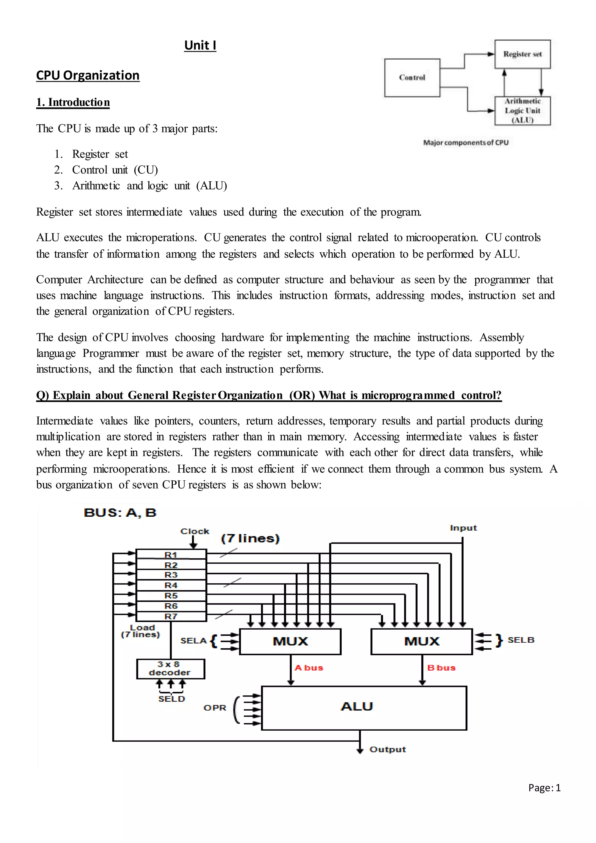
The CPU is made up of 3 major parts: the register set, control unit, and arithmetic logic unit. The register set stores intermediate values during program execution. The control unit generates control signals and selects operations for the ALU. The ALU performs arithmetic and logic operations. Computer architecture includes instruction formats, addressing modes, instruction sets, and CPU register organization. Registers are organized in a bus structure to efficiently transfer data and perform microoperations under control of the control unit. Common instruction fields are the operation code, address fields, and addressing mode fields. Instructions can be classified by the number of address fields as zero-address, one-address, two-address, or three-address instructions. Common addressing modes specify how operands

![Page:2
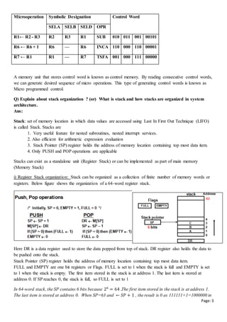
The above diagram consists of 7 registers which are connected to 2 multiplexers (MUX) to form Bus A and
Bus B. The select lines (SELA and SELB ) are used to select the registers to input data to ALU through Bus
A and Bus B.
The ALU performs arithmetic and logical microoperations and generates output. One copy of the output is
stored in the register .
The combined value of SELA( 3bits), SELB( 3bits), SELD( 3bits), OPR (5 bits) (i.e, 3+3+3+5= 14 bits ) is
called control word.
SELA and SELB selects input registers,
SELD selects the output register.
OPR selects the operation to be performed by ALU.
Encoding of register selectionfields
Binary Code SELA SELB SELD
000 Input Input None
001 R1 R1 R1
010 R2 R2 R2
011 R3 R3 R3
100 R4 R4 R4
101 R5 R5 R5
110 R6 R6 R6
111 R7 R7 R7
Encoding of ALU operations
OPR Select Operation Symbol
00000
00001
00010
00101
00110
Transfer A
Increment A
Add A + B
Subtract A – B
Decrement A
SFA
INCA
ADD
SUB
DECA
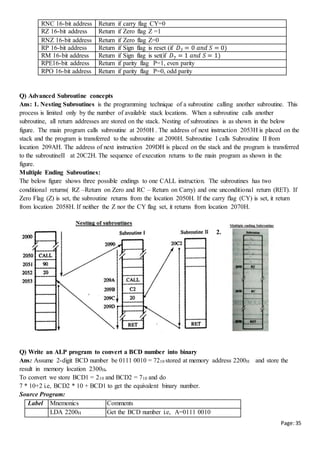
Example of micro operation
The following statements demonstrate the sequence of steps that are used to perform microoperation.
For Example to perform the operation R1 R2 + R3 , the sequence of steps will be
[1] MUX A selector (SELA): Here BUS A R2
[2] MUX B selector (SELB): Here BUS B R3
[3] ALU operation selector (OPR): Here 00010 is fed through OPR to perform addition by ALU.
[4] Decoder destination selector (SELD): Selects the register that must store the output. This is decided by
the SELD input given to 3x8 decoder .Here Output generated after the execution of micro operation is
loaded into R1 .
Field: SELA SELB SELD OPR
Symbol: R2 R3 R1 ADD
Control word: 010 011 001 00010](https://image.slidesharecdn.com/compautosaved-160823141145/85/Computer-Organization-and-8085-microprocessor-notes-2-320.jpg)
![Page:4
binary. But SP =0 as SP can hold 6 least significant bits(LSB). Also when SP=0 and 𝑆𝑃 ← 𝑆𝑃 − 1 then
000000-1=111111 therefore, SP=63.
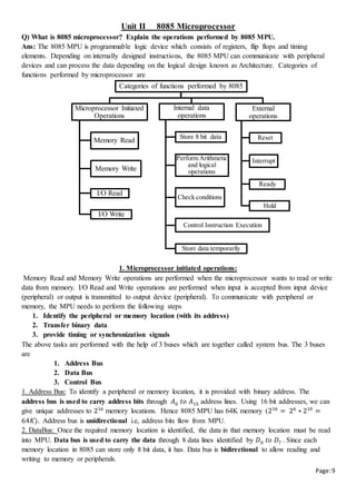
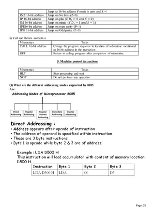
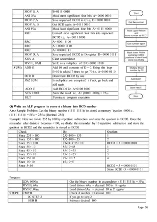
ii) Memory Stack Organization
A portion of main memory is used as stack and processor register as SP. Below figure shows portion of
main memory divided into 3 segments -program, data and stack segments. The initial value of SP is 4001
and the stack grows with decreasing addresses.
Thus the first item stored in the stack is at address
4000, the second item is stored at address 3999, and
the last address that can be used for the stack is 3000.
A new item is inserted with push operation as follows
- PUSH operation: SP SP - 1
M[SP] DR
An data item is deleted using pop operations as
follows
- POP operation: DR M[SP]
SP SP + 1
Most computers do not provide hardware to check stack overflow (full stack) or underflow (empty stack).
Limit checking must be done in software using 2 processor registers. One register to hold upper limit (i.e,
3000 in this case) and another to hold lower limit.
Stack Organization is good for evaluating arithmetic expressions. Common arithmetic expressions are
written in infix notation.
A + B Infix notation
+ A B Prefix or Polish notation
A B + Postfix or reverse Polish notation
Evaluation of Arithmetic Expressions: Any arithmetic expression can be expressed in parenthesis-free
Polish notation. The reverse Polish notation is very suitable for stack. In reverse polish notation operands
are declared first and then the operators. Multiplication and division are performed before addition and
subtraction. The following diagram represents evaluation of arithmetic expression using stack.
The above expression is evaluated from left to right. The operands are pushed onto the stack and the
arithmetic operations are performed on the top 2 elements of the stack, the result is again pushed back onto
stack.
Q) Convert the expression from infix to post fix or reverse polish notation](https://image.slidesharecdn.com/compautosaved-160823141145/85/Computer-Organization-and-8085-microprocessor-notes-4-320.jpg)
![Page:5
Ans: Consider the expression (A + B) * [C * (D + E) + F]
we must first perform the arithmetic inside the parentheses (A + B) and (D + E). So, AB+DE+
Next we must calculate the expression inside the square brackets.
The multiplication of C * (D + E) must be done prior to the addition of F since multiplication has
precedence over addition. So, AB+DE+C*F+
The last operation is the multiplication of the two terms between the parentheses and brackets
The converted expression is A B + D E + C * F + *
The expression can be converted to reverse Polish notation, without the use of parentheses, by taking
into consideration the operation hierarchy.
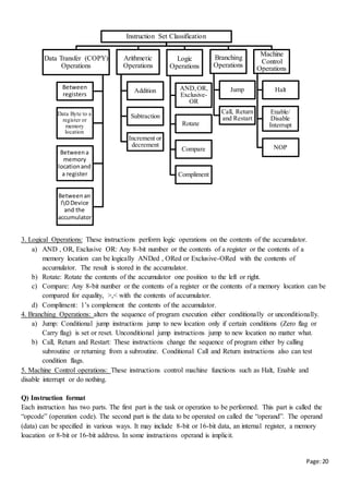
Q) What are the common fields found in an instruction?
Ans: The bits of the instruction are divided into groups called fields. The most common fields found in
instruction formats are:
1. operation code field (op-code field) that specifies the operation to be performed.
2. An address field that has a memory address or a processor register depending on mode field.
3. A addressing mode field that specifies determines how the address field is to be interpreted (to get
effective address or the operand)
Q) Explain about the most common processor organizations. (or) What are 1-address , 2- address, 3-
address and zer-address instructions. (or) Explain about various types of instruction formats.
Ans:
Most common fields in instruction are op-code field, address field and addressing mode field. The number
of address fields in the instruction format depends on the internal organization of CPU. Most computers fall
into one of the 3 types of CPU organizations. They are
1. Single register (Accumulator) organization
2. General register organization
3. Stack organization
1. Single register (Accumulator) organization: Accumulator is the only general purpose register.
Example : ADD X /* AC AC + M[X] */ One address instruction
here AC is the accumulator and M[X] is the memory word located at address X. Since the instruction has
one address field, ADD X is a one –address instruction
2. General register organization employs two or three address fields in their instruction format. Each address
field may specify a processor register or a memory word. Any of the registers can be used as the source or
destination for computer operations.
ADD R1, R2, R3 /* R1 R2 + R3 */
ADD R1, R2, R3 is three address instruction as it has 3 register address fields R1,R2 and R3. First address
field R1 is destination and remaining address fields(R2 and R3) are sources.
ADD R1, R2 /* R1 R1 + R2 */
MOV R1, R2 /* R1 R2 */
ADD R1, X /* R1 R1 + M[X] */
the above 3 instructions are 2 address instructions as they have 2 address fields.](https://image.slidesharecdn.com/compautosaved-160823141145/85/Computer-Organization-and-8085-microprocessor-notes-5-320.jpg)
![Page:6
3. Stack organization: All operations are done using the hardware stack. have PUSH and POP instruction
which require an address field. Thus the instruction
PUSH X /* TOS M[X] */
will push the word at address X to the top of the stack. The stack pointer is updated automatically
The instruction ADD
in stack consists of an operation code only with no address field. Hence ADD is a zero address instruction.
This operation will pop the top 2 data items from the stack, adds them and pushes the sum into the stack
Q) Write a program to execute X = (A + B) * (C + D) using zero, one, two, three address instructions
Ans:
Three-Address Instructions
ADD R1, A, B R1 ← M[A] + M[B]
ADD R2, C, D R2 ← M[C] + M[D]
MUL X, R1, R2 M[X] ← R1 * R2
The advantage of the three-address format is that it results in short programs
The disadvantage is that the binary-coded instructions require too many bits to specify three addresses
Two-Address Instructions
The first symbol listed in an instruction is assumed to be both a source and the destination where the result
of the operation is transferred
One- Address Instructions
LOAD A AC M[A]
ADD B AC AC + M[B]
STORE T M[T] AC
LOAD C AC M[C]
ADD D AC AC + M[D]
MUL T AC AC * M[T]
STORE X M[X] AC
T is the address of a temporary memory location required for storing the intermediate result
Zero Address instruction
MOV R1, A R1 M[A]
ADD R1, B R1 R1+M[B]
MOV R2, C R2 M[C]
ADD R2, D R2 R2 + M[D]
MUL R1, R2 R1 R1 * R2
MOV X, R1 M[X] R1](https://image.slidesharecdn.com/compautosaved-160823141145/85/Computer-Organization-and-8085-microprocessor-notes-6-320.jpg)
![Page:7
TOS stands for top of stack
Q) Explain the different Addressing modes with an example
Ans: Addressing modes are used to find the mode of accessing address of operand for processing the
instruction. The most common addressing modes are:
1. Implied Addressing mode.
2. Immediate Addressing Mode.
3. RegisterAddressing Mode
4. RegisterIndirect Addressing Mode
5. Auto-increment or Auto-decrement Addressing
6. Direct Addressing Mode
7. Indirect Addressing Mode
8. Relative Addressing Mode
9. Indexed Addressing Mode
10. Base RegisterAddressing Mode
1. Implied addressing Mode:
In this mode the operands are specified implicitly in the definition of the instruction.
For example, CMA "complement accumulator“
The operand is the accumulator register and the contents of accumulator are complimented and the
complimented result is again stored in accumulator.
Zero-address instructions in a stack-organized computer are implied-mode instructions since the operands
are implied to be on top of the stack.
2. Immediate addressing Mode:
In this mode the operand is specified in the instruction itself.
In other words, an immediate-mode instruction has an operand field rather than an address field.
For example, MVI A, 50 A ←50
This instruction stores the constant value 50 in accumulator register.
3. Register Addressing Mode:
In this mode the operands are in registers that reside within the CPU.
For example, Add R1,R2 R1← R1 + R2
4. Register Indirect Mode:
In this mode the register contains the address of operand in memory i.e, the instruction specifies the registers
in CPU, these register contains the address of operand.
For example: LDA (R1) AC ← M[R1]
5. Auto increment or Auto Decrement mode:
PUSH A TOS A
PUSH B TOS B
ADD TOS (A + B)
PUSH C TOS C
PUSH D TOS D
ADD TOS (C + D)
MUL TOS (C + D) * (A + B)
POP X M[X] TOS](https://image.slidesharecdn.com/compautosaved-160823141145/85/Computer-Organization-and-8085-microprocessor-notes-7-320.jpg)
![Page:8
This mode is useful to access table of data in memory. When the address stored in the register refers to a
table of data in memory, it is necessary to increment or decrement the register after every access to the table.
This mode is similar to register indirect mode except that the register is incremented or decremented after
the value of memory is accessed
An example for Auto-increment, LDA (R1)+
– AC ← M[R1]
– R1 ← R1+1
An example for Auto-decrement, LDA -(R1)
– R1 ← R1-1
– AC ← M [R1]
6. Direct addressing mode
The operand resides in memory and its address is given directly in the address field of the instruction.
— For example, LDA 4002 AC ← M[4002]
here 4002 is the value in address field of instruction
In this mode the effective address is equal to the address part of the instruction. Here
Effective address is address of operand.
7. Indirect addressing mode:
In this mode the address field of the instruction gives the address where the effective address is stored in
memory.
— For example, LDA @4002 AC ← M[ M[4002] ]
here 4002 is the value in address field of instruction
8. Relative Address Mode:
In this mode the content of the program counter is added to the address part of the instruction in order to
obtain the effective address.
— For example, LDA $ 40 AC ←M[PC+40]
here 40 is the value in address field of instruction
9. Indexed Addressing Mode:
In this mode the content of an index register XR is added to the address part of the instruction to obtain the
effective address.
— For example, LDA add(x) AC ← M[XR+address field value]
Index register is a special CPU register that contains an index value which is automatically incremented after
its contents are accessed. The address field of instruction defines the beginning address of array in memory.
10. Base Register Addressing Mode:
In this mode the content of a base register is added to the address part of the instruction to obtain the e
ffective address. This is similar to the indexed addressing mode except that the register is now called a base
register whose values are not automatically incremented.](https://image.slidesharecdn.com/compautosaved-160823141145/85/Computer-Organization-and-8085-microprocessor-notes-8-320.jpg)
![Page:21
Q) Explain the instruction set supported by 8085
Ans: Since the 8085 is an 8-bit device it can have up to 28 (256) instructions. However, the 8085 only uses
246 combinations that represent a total of 74 instructions. Most of the instructions have more than one
format.
The following notations are used
R = 8085 8-bit register (A, B, C, D, E, H, L)
M = Memory register , it contains data at address present in HL register
Rs = Source Register (A, B, C, D, E, H, L)
Rd = Destination Register (A, B, C, D, E, H, L)
Rp = Register Pair (BC, DE, HL, SP)
[ ] = Contents of
1. Data transfer instructions
Mnemonics Tasks Addressing
mode
Instruct
ion
Size
Example
MOV Rd, Rs Copy data in Rs into Rd.
[ 𝑅𝑑] ← [𝑅𝑠]
Register 1- byte
MOV B, C
MOV R, M Copy data from M into R
[𝑅] ← [𝐻𝐿]
Register
Indirect
1-byte Instruction: LXI H, 2034H
[HL] = 2034H,
[2034] = 58H & [B] = C5H
Instruction: MOV B,M
After execution: [B] = 58H
& M = 58 H
MOV M, R Copy data from R into M.
[𝐻𝐿] ← [𝑅]
Register
Indirect
1-byte
MVI R, 8-bit data Load 8-bit data into R.
[ 𝑅] ←8-bit data
Immediate 2-byte MVI C, 05H
LXI Rp, 16 bit data Loads 16-bit data into Rp.
[ 𝑅𝑝] ←16-bit data
Immediate 3-byte LXI B, D500 H
[B] =D5H & [E]=00H](https://image.slidesharecdn.com/compautosaved-160823141145/85/Computer-Organization-and-8085-microprocessor-notes-21-320.jpg)
![Page:22
LDA 16-bit address Load accumulator with data at given
16-bit address.
[ 𝐴] ← [16-bit address]
Direct 3-byte LDA 9580 H
[9580]=05H
After execution:
[A] =05H
STA 16-bit addre Store the data in accumulator at
given 16-bit address.
[16-bit address] ← [𝐴]
Direct 3-byte STA 9580 H
[A] =05H
After execution:
[9580]=05H
LDAX Rp Load accumulator with the data
present in address stored in Rp
[𝐴] ← [𝑅𝑝]
Register
Indirect
3-byte Let B = 35H & C = 45H
& 3545 location has 22H
Instruction: LDAX B
A = 22H
STAX Rp Store the data in accumulator at
address contained in Rp.
[𝑅𝑝] ← [𝐴]
Register
Indirect
3-byte Let B = 35H & C = 45H
& A = 22H
Instruction: STAX B
3545 location has 22H
OUT 8-bit port
address
Write the data in accumulator to
output device that has 8-bit port
address
Direct 2 byte OUT 07H
IN 8-bit port
address
Accept data from input device that
has 8-bit port address and store it in
accumulator
Direct 2 byte IN 02H
LHLD 16 bit
address
Load HL register with 16bit address.
L ← data stored in 16-bit address.
H ← data stored in 16-bit address+1
Direct 3 bytes Let [C050] = 28 H &
[C051] = 66 H
Instruction: LHLD C050H
After execution:
[H] = 66H & [L] = 28 H
SHLD 16 bit
address
data in 16-bit address ← L
data in 16-bit address+1 ← H
Direct 3 bytes
XCHG [H] ↔ [D]
[L] ↔ [E]
Register 1 byte
2. Arithmetic instructions:
In ADD R, ADD M, SUB R, SUB M, ADI, SUI all the flags are affected.
Mnemonics Tasks Addressing
mode
Instructi
on Size
Example
ADD R Add the contents of R with contents of
accumulator. Result is stored in
accumulator. [A]← [ 𝐴] + [𝑅]
Register 1 byte Let [C] = 05H , [A] =03H
Instruction: ADD C
After execution:
[A] =08H
ADD M Add the contents of M with contents of
accumulator. Result is stored in
accumulator. [A]← [ 𝐴] + [𝐻𝐿]
Register
Indirect
1 byte [HL] = 2034H,
[2034] = 05H & [A] = 03H
Instruction: ADD M
After execution:
[A] = 08H & M = 05 H
SUB R Subtract the contents of R from contents
of accumulator. [ 𝐴] ← [ 𝐴] − [𝑅]
Register 1 byte
SUB M Subtract the contents of R from contents
of accumulator. [ 𝐴] ← [ 𝐴] − [𝐻𝐿]
Register
Indirect
1 byte
ADI 8-bit data Add 8-bit data to contents of
accumulator. [A]← [ 𝐴] + 8-bit data
Immediate 2 bytes [A] = 03H
Instruction: ADI 05 H
After execution: [A] = 08H
SUI 8-bit data Subtract 8-bit data from the contents of
accumulator. [A]← [ 𝐴] − 8-bit data
Immediate 2 bytes
INR R Increment contents of R by 1
[𝑅] ← [ 𝑅] +1
Register 1 byte All flags except carry flag
are affected. [C] = FF H
Instruction: INR C
After execution: [C] = 00H](https://image.slidesharecdn.com/compautosaved-160823141145/85/Computer-Organization-and-8085-microprocessor-notes-22-320.jpg)
![Page:23
DCR R Decrement contents of R by 1
[ 𝑅] ← [ 𝑅] −1
Register 1 byte All flags except carry flag
are affected
INR M Increment the contents of M by 1
[ 𝐻𝐿] ← [ 𝐻𝐿] +1
Register 1 byte All flags except carry flag
are affected
DCR M Decrement the contents of M by 1
[ 𝐻𝐿] ← [ 𝐻𝐿] −1
Register 1 byte All flags except carry flag
are affected.
Let [HL] = F050H &
[F050] = 05H
Instruction: DCR M
After execution: [F050] = 04H
INX Rp Increment the contents of Rp by 1
[ 𝑅𝑝] ← [ 𝑅𝑝] +1
Register 1 byte No flags effected
Let [HL] = F050H
Instruction: INX H
After execution: [HL]=F051H
DCX Rp Decrement contents of Rp by 1
[ 𝑅𝑝] ← [ 𝑅𝑝] −1
Register 1 byte No flags effected
DAD Rp [ 𝐻𝐿] ← [ 𝐻𝐿]+ [𝑅𝑝] Register 1 byte Only carry flag affected
3. Logical Instructions:
Logical instructions
implicitly assume accumulator as one of the operand and the result is stored in accumulator.
modifies Z, P, S flags according to the result
resets CY flag. (except CMA instruction : CMA does not affect any flags
Do not affects the operand register.
Mnemonics Tasks Addressing
mode
Inst.
Size
ANA R/M Logically AND [R] /[M] with [A] Register/Register
indirect
1-byte
ORA R/M Logically OR [R]/[M] with [A] Register/Register
indirect
1-byte
XRA R/M Logically Exclusive-OR [R] / [M] with [A] Register/Register
indirect
1-byte
ANI 8-bit data Logically AND 8-bit data with [A] Immediate 2-byte
ORI 8-bit data Logically OR 8-bit data with [A] Immediate 2-byte
XRI 8-bit data Logically Exclusive-OR 8-bit data with [A] Immediate 2-byte
CMA Compliment [A] Implied 1-byte
CMP R/M Compare [R/M] with [A] for < , > or =
if [A] < [R/M]: carry flag is set
if [A] = [R/M]: zero flag is set
if [A] > [R/M]:: carry and zero flags are reset.
Example:CMP B or CMP M
Register/Register
indirect
1-byte
CPI 8-bit data Compare 8-bit data with [A] for < , > or =
The values being compared remain unchanged.
The result of the comparison is shown by setting the flags
of the PSW as follows:
if [A] < data: carry flag is set
if [A] = data: zero flag is set
if [A] > data: carry and zero flags are reset
Example: CPI 89H
Immediate 2-byte
RLC Rotate accumulator left Implied 1-byte](https://image.slidesharecdn.com/compautosaved-160823141145/85/Computer-Organization-and-8085-microprocessor-notes-23-320.jpg)
![Page:24
Rotate [A] to left by 1-bit
RRC Rotate accumulator right
Rotate [A] to right by 1-bit
Implied 1-byte
RAL Rotate accumulator left through carry Implied 1-byte
RAR Rotate accumulator right through carry Implied 1-byte
4. Branching Instructions:
The branching instruction are classified into 3 categories
Jump instructions
Call and Return instructions
Restart instructions
i) Jump instructions: have an instruction size of 3 bytes. All these instruction have immediate addressing
mode. Jump instructions are of two types
a) Unconditional Jump instructions : Example
Mnemonics Tasks
JMP 16-bit address Jump to 16-bit address unconditionally
b) Conditional Jump instructions
Mnemonics Tasks
JC 16-bit address Jump on carry
Jump to 16-bit address if result generates carry and CY =1
JNC 16-bit address Jump on No Carry (CY=0)
JZ 16-bit address Jump on Zero](https://image.slidesharecdn.com/compautosaved-160823141145/85/Computer-Organization-and-8085-microprocessor-notes-24-320.jpg)
![Page:27
Q) Write an Assembly language program(ALP) to perform 1’s compliment on 8-bit number.
Ans:
Input: is 0FH stored at memory location 4500H
Let us store the complemented number at memory location 4600H.
Source program:
LDA 4500H ; Load Accumulator with data in the location 4500H
CMA ;Complement the number
STA 4600H ;Store the result in accumulator to location 4600H
HLT ;Terminate program execution
Output: Result = F0H is stored at memory location 4600H
Q) Write an Assembly language program(ALP) to perform 2’s compliment on 8-bit number.
Ans: Input : is 0FH stored at memory location 4500H
Let us store the result at memory location 4600H.
Source program:
LDA 4500H ; Load Accumulator with data in the location 4500H [𝐴] ← 0𝐹 H
CMA ;Complement the number [𝐴] ← 𝐹0H
INR A ; Increment the contents of accumulator [𝐴] ← 𝐹1H
STA 4600H ;Store the result in accumulator to location 4600H [4600] ← 𝐹1 H
HLT ;Terminate program execution
Output: Result = F1H is stored at memory location 4600H
Q) Write an Assembly language program(ALP) to perform 2’s compliment
on 16-bit number.
Ans:Let input 16- bit number be 050FH
Address Contents
3000 05H Lower byte of input number
3001 0FH Higher byte of input number
LHLD 3000H ;Load H-L pair with operand from 3000H.
[ 𝐿] ← 𝑐𝑜𝑛𝑡𝑒𝑛𝑡𝑠 𝑜𝑓 𝑚𝑒𝑚𝑜𝑟𝑦 𝑙𝑜𝑐𝑎𝑡𝑖𝑜𝑛 3000
[ 𝐻] ← 𝑐𝑜𝑛𝑡𝑒𝑛𝑡𝑠 𝑜𝑓 𝑚𝑒𝑚𝑜𝑟𝑦 𝑙𝑜𝑐𝑎𝑡𝑖𝑜𝑛 3001 i.e,
[𝐻] ← 05H [𝐿] ← 0𝐹 H
MOV A, L ;Move the lower-order from reg. L to reg. A. [𝐴] ← 0𝐹 H
CMA ;Complement accumulator. [𝐴] ← 𝐹0H
MOV L, A ;Move the result from reg. A to reg. L. [𝐿] ← 𝐹0H
MOV A, H ;Move the higher-order from reg. H to reg. A. [𝐴] ← 05 H
CMA ;Complement accumulator. [𝐴] ← 𝐹𝐴 H
MOV H, A ;Move the result from reg. A to reg. H. [𝐻] ← 𝐹𝐴H
INX H ;Increment H-L pair. [𝐿] ← 𝐹1 H
SHLD 3002H ;Store the result at address 3002H. [3002H] ← [𝐿]
[3003H] ← [𝐻]
HLT ;Halt.
Output: Result : F1FAH
Address Contents
3002 F1H Lower byte of result](https://image.slidesharecdn.com/compautosaved-160823141145/85/Computer-Organization-and-8085-microprocessor-notes-27-320.jpg)
![Page:28
3003 FAH Higher byte of result
Q) Write an Assembly language program(ALP) to perform 1’s compliment on 16-bit number.
Ans:Let input 16- bit number be 050FH
Address Contents
3000 05H Lower byte of input number
3001 0FH Higher byte of input number
Program:
LHLD 3000H ;Load H-L pair with operand from 3000H. [𝐻] ← 05H
[𝐿] ← 0𝐹 H
MOV A, L ;Move the lower-order from reg. L to reg. A. [𝐴] ← 0𝐹 H
CMA ;Complement accumulator. [𝐴] ← 𝐹0H
MOV L, A ;Move the result from reg. A to reg. L. [𝐿] ← 𝐹0H
MOV A, H ;Move the higher-order from reg. H to reg. A. [𝐴] ← 05 H
CMA ;Complement accumulator. [𝐴] ← 𝐹𝐴 H
MOV H, A ;Move the result from reg. A to reg. H. [𝐻] ← 𝐹𝐴H
SHLD 3002H ;Store the result at address 3002H. [3002H] ← [𝐿]
[3003H] ← [𝐻]
HLT ;Halt.
Output: Result : F0FAH
Address Contents
3002 F0H Lower byte of result
3003 FAH Higher byte of result
Q) Write an Assembly language program(ALP) to perform addition of two 8-bit numbers.
Ans:
Input: First 8-bit number is 05H stored at memory location 4500H
Second 8-bit number is 03H stored at memory location 4501H
Let us store the result at memory location 4600H.
Source program:
Label Mnemonics Comments
MVI C, 00H ;Clear C register to hold carry
[𝐶] ←00H
LDA 4500H ; [ 𝐴] ← [4500] 𝑖. 𝑒, [𝐴] ← 05H
MOV B, A ; copy the contents of A into B [𝐵] ← 05 H
LDA 4501H ;[ 𝐴] ← [4501] 𝑖. 𝑒, [𝐴] ← 03H
ADD B ; [ 𝐴] ← [ 𝐴] + [𝐵] i.e, [ 𝐴] ← 08H
JNC LOOP ; jump if no carry to label LOOP
INR C Increment carry
LOOP: STA 4600H ;Store the addition result at address 4600 i.e,
[4600] ← [𝐴]
MOV A, C ; [ 𝐴] ← [𝐶]
STA 4601H ; store carry at address 4601 i.e, [4600] ← [𝐶]
HLT ;Halt
Output: Result = 08H and Carry =00 H
Before
Execution:
After Execution:
4500H: 05H 4600H: 08H
4501H: 03H 4601H: 00H](https://image.slidesharecdn.com/compautosaved-160823141145/85/Computer-Organization-and-8085-microprocessor-notes-28-320.jpg)
![Page:29
Q) Write an Assembly language program(ALP) to perform addition of two 16-bit numbers.
Ans: Let first 16- bit number be 0105H and second number be 0203H
Address Contents
3000 05H Lower byte of first number
3001 01H Higher byte of first number
3002 03H Lower byte of second number
3003 02H Higher byte of second number
Label Mnemonics Comments
MVI C, 00H ;Clear C register to hold carry
[𝐶] ←00H
LHLD 3000H ;Load H-L pair with operand from 3000H.
[ 𝐿] ← 𝑐𝑜𝑛𝑡𝑒𝑛𝑡𝑠 𝑜𝑓 𝑚𝑒𝑚𝑜𝑟𝑦 𝑙𝑜𝑐𝑎𝑡𝑖𝑜𝑛 3000
[ 𝐻] ← 𝑐𝑜𝑛𝑡𝑒𝑛𝑡𝑠 𝑜𝑓 𝑚𝑒𝑚𝑜𝑟𝑦 𝑙𝑜𝑐𝑎𝑡𝑖𝑜𝑛 3001 i.e,
[𝐻] ← 01H [𝐿] ← 05H
XCHG ; [H] ↔ [D] [L] ↔ [E]
[𝐷] ← 01 H [𝐸] ← 05 H
LHLD 3002H ;[ 𝐿] ← 𝑐𝑜𝑛𝑡𝑒𝑛𝑡𝑠 𝑜𝑓 𝑚𝑒𝑚𝑜𝑟𝑦 𝑙𝑜𝑐𝑎𝑡𝑖𝑜𝑛 3002
[ 𝐻] ← 𝑐𝑜𝑛𝑡𝑒𝑛𝑡𝑠 𝑜𝑓 𝑚𝑒𝑚𝑜𝑟𝑦 𝑙𝑜𝑐𝑎𝑡𝑖𝑜𝑛 3003 i.e,
[𝐻] ← 02H [𝐿] ← 03H
DAD D ;Add HL pair with DE pair
[ 𝐻] ← [ 𝐻] + [ 𝐷] and [ 𝐿] ← [ 𝐿] + [ 𝐸] i.e,
[ 𝐻] ← 03H and [ 𝐿] ←08H
JNC LOOP ; jump if no carry to label LOOP
INR C ;Move the result from reg. A to reg. H. [𝐻] ← 𝐹𝐴H
LOOP: SHLD 4600H ; Store the result at address 4600H. [4600H] ← [𝐿]
[4601H] ← [𝐻]
MOV A,C ; [ 𝐴] ← [𝐶]
STA 4602 H ; store carry at address 4601 i.e, [4602] ← [𝐶]
HLT ;Halt.
Output: Result = 0308H and carry =0
Address Contents
4600 08H Lower byte of addition result
4601 03H Higher byte of addition result
4602 00H Carry
Q) Write an Assembly language program(ALP) to perform multiplication of two 8-bit numbers.
Ans: To perform 02 H * 05H the following ALP is written
Label Mnemonic Comment
MVI C, 00H ;Clear C register [𝐶] ←00H
MVI A, 02H ;[A] ←02 H
MOV B, A ; [B] ←02 H
MVI A, 05H [A] ←05 H
MOV D, A ;[D] ← [𝐴] i.e, [ 𝐷] ←05 H here D is multiplier = 05 H
MVI A, 00H ;Clear accumulator [A] ←00 H
SUM: ADD B ; [A] ← [ 𝐴] + [𝐵]
JNC DEC ;Jump if no carry to label DEC
INR C ; [ 𝐶] ← [ 𝐶]+ 1](https://image.slidesharecdn.com/compautosaved-160823141145/85/Computer-Organization-and-8085-microprocessor-notes-29-320.jpg)
![Page:30
DEC: DCR D ; [D] ← [ 𝐷] − 1
JNZ SUM ; Jump if D is not equal to zero to Label SUM
STA 4600H ; Store the result at address 4600H
MOV A,C ;Move carry in C to A
STA 4601H ;Store carry at address 4601H
HLT ;Halt
Output: Result = 0AH and carry =00H
Q) Write an Assembly language program(ALP) to perform Multiplication of two 16-bit numbers.
Ans: 0002H * 0005H
Address Contents
3000 02H Lower byte of first number
3001 00H Higher byte of first number
3002 05H Lower byte of second number
3003 00H Higher byte of second number
Label Mnemonics Comments
MVI C, 00H ;Clear C register [𝐶] ←00H
LHLD 3000H ;Load H-L pair with operand from 3000H.
SPHL ;[ 𝑆𝑃] ← [ 𝐻𝐿]
LHLD 3002H ; Load H-L pair with operand from 3000H.
XCHG ; [H] ↔ [D] [L] ↔ [E]
MVI L, 00H
MVI H, 00H
SUM: DAD SP ;Add HL pair with SP [ 𝐻𝐿] ← [ 𝐻𝐿] + [ 𝑆𝑃]
JNC DEC ;Jump if no carry to label DEC
INX C ; [ 𝐶] ← [ 𝐶] + 1
DEC: DCX D ; [DE] ← [ 𝐷𝐸] − 1
JNZ SUM ; Jump if DE is not equal to zero to Label SUM
LOOP: SHLD 4600H ; Store the result at address 4600H. [4600H] ← [𝐿]
[4601H] ← [𝐻]
MOV A,C ; [ 𝐴] ← [𝐶]
STA 4602 H ; store carry at address 4601 i.e, [4602] ← [𝐶]
HLT ;Halt.
Output: Result = 0008H and carry =0
Address Contents
4600 08H Lower byte of addition result
4601 00H Higher byte of addition result
4602 00H Carry
Q) Write an Assembly language program (ALP) to find Sum of series.
Ans: The length of the series is in memory location 4200 H and
the series begins from memory location 4201 H.
Sample problem:
Address Contents
4600 0AH Result
4601 00H Carry
Address Content
4200 H 03 H Size of series
4201 H 02 H First element in series
4202 H 05 H Second element in series
4203 H 03 H Third element in series](https://image.slidesharecdn.com/compautosaved-160823141145/85/Computer-Organization-and-8085-microprocessor-notes-30-320.jpg)
![Page:31
Source program:
Result =02+05+03= 0A H . The Result is stored at 4300 H = 0A H
Q) Write an Assembly language program (ALP) to perform sorting
Ans:
Before Execution:
Address Content
4200 H 03 H Size of array
4201 H 02 H First element in array
4202 H 05 H Second element in array
4203 H 03 H Third element in array
Source Program:
Label Mnemonics Comment
LXI H,4200
MOV C,M
DCR C
REPEAT: MOV D,C
LXI H,4201
LOOP: MOV A,M
INX H
CMP M
JC SKIP
MOV B,M
MOV M,A
DCX H
MOV M,B
INX H
SKIP: DCR D
JNZ LOOP
DCR C
JNZ REPEAT
HLT
After Execution:
Label Mnemonic Comment
LDA 4200H
MOV C, A ; store the size of array in C
MVI A, 00H
LXI H, 4201 H ;HL register stores the address 4201
BACK: ADD M ;M register contains the data at 4201
[ 𝑀] ← [4201]i.e, [ 𝑀] ← 02H
INX H HL register increments to 4202
DCR C
JNZ BACK
STA 4300 H
HLT
Address Content
4200 H 03 H Size of series
4201 H 02 H First element in array after sorting](https://image.slidesharecdn.com/compautosaved-160823141145/85/Computer-Organization-and-8085-microprocessor-notes-31-320.jpg)
![Page:32
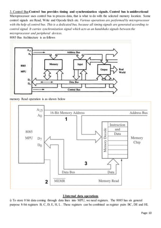
Q) Explain about Stack concept in 8085
Ans: Stack in 8085 is a memory stack i.e, a set of memory locations in main memory is reserved for
stack.The beginning of the stack is defined in program using the instruction.
LXI SP, 16-bit address.
Storing of data bytes begins at memory address one less than the address in stack pointer register.
For Example : If a program is running, it is placed in main memory. If program memory ranges from 2000
to 23FF, SP is initialized to 2400 i.e, (1+23FF) i.e, one address beyond the program memory. Information is
saved on the stack by PUSHing it on. It is retrieved from the stack by POPing it off. The 8085 provides two
instructions: PUSH and POP for storing information on the stack and retrieving it back. Both PUSH and
POP work with register pairs ONLY.
PUSH instructions in Stack: PUSH B, PUSH D, PUSH H, PUSH PSW instructions are 1-byte
instructions. Here PSW means program status word. Accumulator and flag register is together called PSW.
Initialization of stack pointer register to 2400H LXI SP,2400H [SP]← 2400H
LXI B, 12F3H [B] ←12H and [C] ←F3H
Decrement SP [SP] ← [SP] -1 [SP]← 23FFH
Copy the contents of register B to the memory location
pointed to by SP
PUSH B M[SP] ← 12H
Decrement SP [SP] ← [SP] -1 [SP]← 23FEH
Copy the contents of register C to the memory location
pointed to by SP
M[SP] ← F3H
PUSH PSW
Decrement SP [SP] ← [SP] -1 [SP]← 23FDH
Copy the contents of Accumulator to the memory
location pointed to by SP
M[SP] ← [A]
Decrement SP [SP] ← [SP] -1 [SP]← 23FCH
Copy the contents Flag register to the memory location
pointed to by SP
M[SP] ← [Flag register]
4202 H 03 H Second element array after sorting
4203 H 05 H Third element in array after sorting](https://image.slidesharecdn.com/compautosaved-160823141145/85/Computer-Organization-and-8085-microprocessor-notes-32-320.jpg)
![Page:33
POP instructions in Stack: POP B, POP D, POP H, POP PSW instructions are 1-byte instructions
[SP]← 23FCH
Copy the contents of the memory location pointed to by
the SP to Flag register
POP PSW [Flag register] ← M[SP]
Increment SP [SP] ← [SP] +1 [SP]← 23FDH
Copy the contents of the memory location pointed to by
the SP to accumulator register
[A] ←M[SP]
Increment SP [SP] ← [SP] +1 [SP]← 23FEH
Copy the contents of the memory location pointed to by
the SP to E register
POP D [E]← F3H
Increment SP [SP] ← [SP] +1 [SP]← 23FFH
Copy the contents of the memory location pointed to by
the SP to D Register
[D]← 12H
Increment SP [SP] ← [SP] +1 [SP]← 2400H
The order of PUSHs and POPs must be opposite of each other in order to retrieve information back into its
original location.
PUSH B
PUSH D
...
POP D
POP B
Reversing the order of the POP instructions will result in the exchange of the contents of BC and DE.
Q) Explain about Subroutine concept in 8085
Ans: A subroutine is a group of instructions that will be used repeatedly. Instead of writing the same
instructions repeatedly, the repeated instructions are written only once as subroutine and called whenever
required. The 8085 has two instructions for dealing with subroutines. The CALL instruction is used to
redirect program execution to the subroutine. The RET instruction is used to return the execution to the
calling routine.
For Example : If a program is running, it is placed in main memory as shown in the figure. In the below
program memory ranges from 2000H to 23FFH, SP is initialized to 2400H.](https://image.slidesharecdn.com/compautosaved-160823141145/85/Computer-Organization-and-8085-microprocessor-notes-33-320.jpg)
![Page:37
INR E update quotient
JMP STEP 1 go to step 1
STEP2: CMP C Check if number < Decimal 10
JC STEP 3 if yes go to step 3
SUB C Subtract decimal 10
INR D Update quotient
JMP STEP 2 Continue division by 10
STEP3: STA 6100H Store Digit 0
MOV A, D Get Digit 1
STA 6101H Store Digit 1
MOV A, E Get Digit 2
STA 6102H Store Digit 2
Output:
Q) Write an ALP program to convert a ASCII HEX to Binary number
Ans:
ASCII stands for American standard code for information interchange. It is a seven bit code and its 128
combinations are assigned different alphanumeric characters. For example: Hexadecimal number 30 H to 39H
represent 0 to 9 ASCII decimal numbers and 41H represents A, 42H represents B, 43H represents C, 44H
represents D, 45H represents E, 46H represents F .....5AH represents Z.
input: ASCII code 41H stored in memory location C200H
Label Mnemonics Comment
LDA C200H ;Load the accumulator with binary number A=0100 0001
SUI 30H ;Subtract immediate data 30H from the contents of
accumulator A= 0001 0001 = (decimal 11)
CPI 0AH ;Compare immediately the accumulator content with 0AH
Since (0001 0001)> (0000 1010) CY = 0
JC ST Jump if carry to label ST
SUI 07 ;Subtract immediate data 07H the contents of accumulator
0001 0001 -0000 0111 =0001 0001+1111 1001 =0000 1010= 0AH
ST: STA C202H ;Store the accumulator content at C202H
Here result = 0AH
HLT ;Halt the execution
Output: 0AH (binary output ) stored at memory location C202H
Q) Write an ALP program to convert Binary to ASCII Hex Code
Ans:
Input: 8-bit binary number 9AH stored at memory location 4050H
Main Program:
Label Mnemonics Comments
LXI SP, 4100H Initialize Stack pointer
LDA 4050H Get the binary number i.e, A=1001 1111
LXI D, 4060H Point index where ASCII code to be stored i.e, [DE] ←4060H
MOV B, A Save byte in B=1001 1010
Memory address Content
6100H
6101H
6102H](https://image.slidesharecdn.com/compautosaved-160823141145/85/Computer-Organization-and-8085-microprocessor-notes-37-320.jpg)
![Page:38
RRC Shift high order nibble to lower order nibble.
A=1100 1111
RRC A= 11100111
RRC A = 1111 0011
RRC A= 1111 1001
CALL ASCII Call Conversion subroutine
STAX D Store first ASCII Hex in 4060H
INX D [DE] ←4061H
MOV A, B Get the input binary number i.e, A=1001 1111
CALL ASCII
STAX D Store Second ASCII Hex in 4061H
HLT Terminate program execution
ASCII: this subroutine converts binary digit between 0 and F to ASCII Hex code.
input: Single binary number in accumulator
output: ASCII Hex code in accumulator
Label Mnemonic Comments First byte Second byte
ANI 0FH Mask most significant four
bits
Before execution:
A=1111 1001
after execution ANI 0FH:
A= 0000 1001=09H
Before execution:
A=1001 1111
after execution ANI 0FH:
A= 0000 1111=0FH
CPI 0AH Is digit less than decimal 10 CY =1 as 09H < 0A H CY =0 as 0FH >0A H
JC CODE If digit less than decimal 10
go to label CODE and add
30 H
ADI 07 H ADD 07 to obtain code for
digits from A to F
A= 0FH +7 H = 16 H
CODE: ADI 30 H Add base number 30 H A= 30H +9 H = 39 H A= 30H +16 H = 46 H
RET Return to calling program
Output
Memory address Content
4060H 39 H ASCII Hex code 39H represents 9 ASCII decimal number
4061H 46 H ASCII Hex code 46H represents F](https://image.slidesharecdn.com/compautosaved-160823141145/85/Computer-Organization-and-8085-microprocessor-notes-38-320.jpg)


![Ise iv-computer organization [10 cs46]-notes new](https://cdn.slidesharecdn.com/ss_thumbnails/ise-iv-computerorganization10cs46-notesnew-140624013827-phpapp01-thumbnail.jpg?width=640&height=640&fit=bounds)