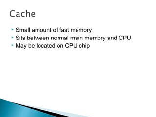
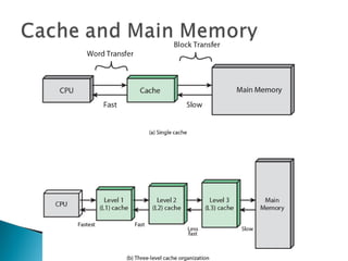
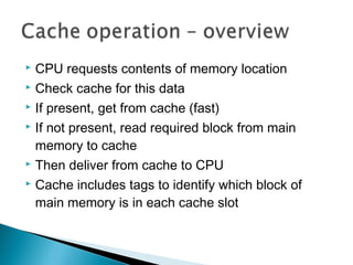
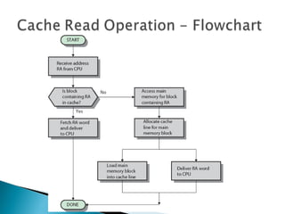
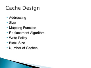
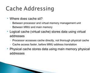
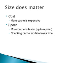
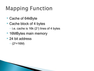
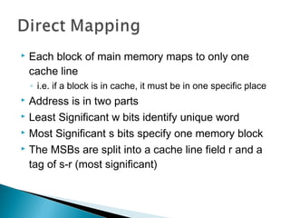
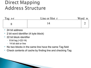
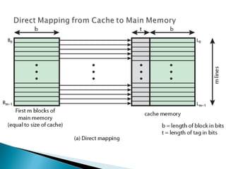
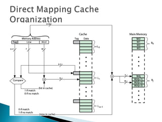
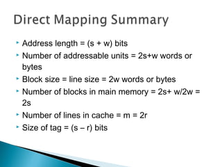
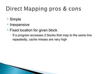
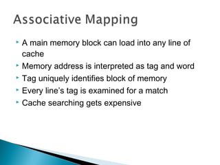
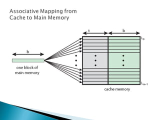
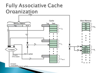
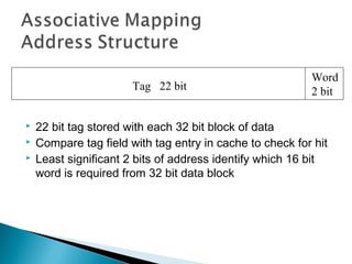
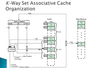
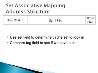
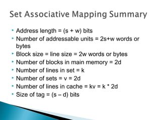
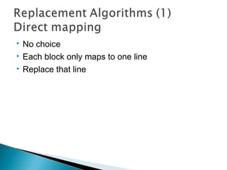
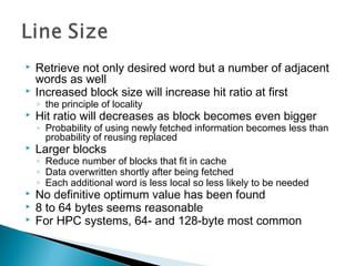
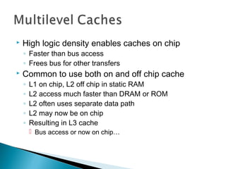
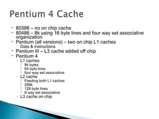
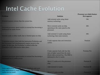
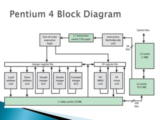
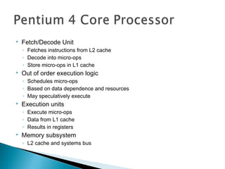
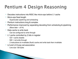
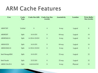
The document discusses cache design and organization. It describes how caches work, sitting between the CPU and main memory to provide fast access to frequently used data. The key aspects covered include cache size, block size, mapping techniques, replacement algorithms, write policies, and the evolution of cache hierarchies in processors like the Pentium IV with multiple levels of on-chip and off-chip caches.
The Presentation introduces the basic concept of cache memory, its introduction , background and all necessary details are provided along with details of different mapping techniques that are used inside Cache Memory.
Memory organization
Memory Organization in Computer Architecture. A memory unit is the collection of storage units or devices together. The memory unit stores the binary information in the form of bits. ... Volatile Memory: This loses its data, when power is switched off.
sensors are what we experience the most in our life. they are even working in our body in different aspects. they may be as eyes, ears, skin, tongue etc. when we combine them they make a network. it may be a human sensor network. but i have shared something interesting about wireless sensor networks.
Modern computationally intensive tasks are rarely bottlenecked by the absolute performance of your processor cores. The real bottleneck in 2013 is getting data out of memory. CPU caches are designed to alleviate the difference in performance between CPU core clock speed and main memory clock speed, but developers rarely understand how this interaction works or how to measure or tune their application accordingly. This session aims to address this by:
• Describing how CPU caches work in the latest Intel hardware
• Showing what and how to measure in order to understand the caching behavior of software
• Giving examples of how this affects Java program performance and what can be done to address poor cache utilization
Introduction of Motorola microprocessors
Designers
Motorola microprocessor family
Motorola 6800 Microprocessor Family
Variations of 6800
Motorola 680x0 Microprocessor Family
Motorola PowerPC Family
Features of MC6800 Microprocessor
Memory of MC6800 Microprocessor
A brief overview of caching mechanisms in a web application. Taking a look at the different layers of caching and how to utilize them in a PHP code base. We also compare Redis and MemCached discussing their advantages and disadvantages.
Computer Architecture – An IntroductionDilum Bandara
Overview on high-level design of internal components of a computer. Cover step-by-step execution of a program through ALU while accessing & updating registers
About Cache Memory
working of cache memory
levels of cache memory
mapping techniques for cache memory
1. direct mapping techniques
2. Fully associative mapping techniques
3. set associative mapping techniques
Cache memroy organization
cache coherency
every thing in detail
This slide contains information about Memory and its parameters,Classification of memory, Allocation policies, cache memory, Virtual memory, Paging, Segmentation and pipelining
2. M. V. Wilkes, “Slave Memories and Dynamic Storage Allocation,”
IEEE Transactions on Electronic Computers, vol. EC-14, no. 2,
pp. 270-271, April 1965.
2
3. Small amount of fast memory
Sits between normal main memory and CPU
May be located on CPU chip
4.
5. CPU requests contents of memory location
Check cache for this data
If present, get from cache (fast)
If not present, read required block from main
memory to cache
Then deliver from cache to CPU
Cache includes tags to identify which block of
main memory is in each cache slot
6.
7. Addressing
Size
Mapping Function
Replacement Algorithm
Write Policy
Block Size
Number of Caches
8.
Where does cache sit?
◦ Between processor and virtual memory management unit
◦ Between MMU and main memory
Logical cache (virtual cache) stores data using virtual
addresses
◦ Processor accesses cache directly, not thorough physical cache
◦ Cache access faster, before MMU address translation
Physical cache stores data using main memory physical
addresses
9.
Cost
◦ More cache is expensive
Speed
◦ More cache is faster (up to a point)
◦ Checking cache for data takes time
10. Cache of 64kByte
Cache block of 4 bytes
◦ i.e. cache is 16k (214) lines of 4 bytes
16MBytes main memory
24 bit address
◦ (224=16M)
11.
Each block of main memory maps to only one
cache line
◦ i.e. if a block is in cache, it must be in one specific place
Address is in two parts
Least Significant w bits identify unique word
Most Significant s bits specify one memory block
The MSBs are split into a cache line field r and a
tag of s-r (most significant)
12. Tag s-r
Line or Slot r
8
14
24 bit address
2 bit word identifier (4 byte block)
22 bit block identifier
◦ 8 bit tag (=22-14)
◦ 14 bit slot or line
No two blocks in the same line have the same Tag field
Check contents of cache by finding line and checking Tag
Word w
2
13.
14.
15. Address length = (s + w) bits
Number of addressable units = 2s+w words or
bytes
Block size = line size = 2w words or bytes
Number of blocks in main memory = 2s+ w/2w =
2s
Number of lines in cache = m = 2r
Size of tag = (s – r) bits
16. Simple
Inexpensive
Fixed location for given block
◦ If a program accesses 2 blocks that map to the same line
repeatedly, cache misses are very high
17. A main memory block can load into any line of
cache
Memory address is interpreted as tag and word
Tag uniquely identifies block of memory
Every line’s tag is examined for a match
Cache searching gets expensive
18.
19.
20. Tag 22 bit
Word
2 bit
22 bit tag stored with each 32 bit block of data
Compare tag field with tag entry in cache to check for hit
Least significant 2 bits of address identify which 16 bit
word is required from 32 bit data block
21. Address length = (s + w) bits
Number of addressable units = 2s+w words or
bytes
Block size = line size = 2w words or bytes
Number of blocks in main memory = 2s+ w/2w =
2s
Number of lines in cache = undetermined
Size of tag = s bits
22. Cache is divided into a number of sets
Each set contains a number of lines
A given block maps to any line in a given set
◦ e.g. Block B can be in any line of set i
e.g. 2 lines per set
◦ 2 way associative mapping
◦ A given block can be in one of 2 lines in only one set
23. 13 bit set number
Block number in main memory is modulo 213
24.
25.
26. Tag 9 bit
Set 13 bit
Use set field to determine cache set to look in
Compare tag field to see if we have a hit
Word
2 bit
27. Address length = (s + w) bits
Number of addressable units = 2s+w words or
bytes
Block size = line size = 2w words or bytes
Number of blocks in main memory = 2d
Number of lines in set = k
Number of sets = v = 2d
Number of lines in cache = kv = k * 2d
Size of tag = (s – d) bits
28. No choice
Each block only maps to one line
Replace that line
29. Hardware implemented algorithm (speed)
Least Recently used (LRU)
e.g. in 2 way set associative
First in first out (FIFO)
◦ replace block that has been in cache longest
Least frequently used
◦ replace block which has had fewest hits
Random
30. Must not overwrite a cache block unless main
memory is up to date
Multiple CPUs may have individual caches
I/O may address main memory directly
31. All writes go to main memory as well as cache
Multiple CPUs can monitor main memory traffic to
keep local (to CPU) cache up to date
Lots of traffic
Slows down writes
Remember bogus write through caches!
32. Updates initially made in cache only
Update bit for cache slot is set when update
occurs
If block is to be replaced, write to main memory
only if update bit is set
Other caches get out of sync
I/O must access main memory through cache
N.B. 15% of memory references are writes
33.
Retrieve not only desired word but a number of adjacent
words as well
Increased block size will increase hit ratio at first
◦ the principle of locality
Hit ratio will decreases as block becomes even bigger
◦ Probability of using newly fetched information becomes less than
probability of reusing replaced
Larger blocks
◦ Reduce number of blocks that fit in cache
◦ Data overwritten shortly after being fetched
◦ Each additional word is less local so less likely to be needed
No definitive optimum value has been found
8 to 64 bytes seems reasonable
For HPC systems, 64- and 128-byte most common
34.
High logic density enables caches on chip
◦ Faster than bus access
◦ Frees bus for other transfers
Common to use both on and off chip cache
◦
◦
◦
◦
◦
L1 on chip, L2 off chip in static RAM
L2 access much faster than DRAM or ROM
L2 often uses separate data path
L2 may now be on chip
Resulting in L3 cache
Bus access or now on chip…
35.
80386 – no on chip cache
80486 – 8k using 16 byte lines and four way set associative
organization
Pentium (all versions) – two on chip L1 caches
◦ Data & instructions
Pentium III – L3 cache added off chip
Pentium 4
◦ L1 caches
8k bytes
64 byte lines
four way set associative
◦ L2 cache
Feeding both L1 caches
256k
128 byte lines
8 way set associative
◦ L3 cache on chip
36. Problem
Solution
Processor on which feature
first appears
Add external cache using faster
memory technology.
386
External memory slower than the system bus.
Increased processor speed results in external bus becoming a
bottleneck for cache access.
Move external cache on-chip,
operating at the same speed as the
processor.
486
486
Internal cache is rather small, due to limited space on chip
Add external L2 cache using faster
technology than main memory
Create separate data and instruction
caches.
Pentium
Create separate back-side bus that
runs at higher speed than the main
(front-side) external bus. The BSB is
dedicated to the L2 cache.
Pentium Pro
Contention occurs when both the Instruction Prefetcher and
the Execution Unit simultaneously require access to the
cache. In that case, the Prefetcher is stalled while the
Execution Unit’s data access takes place.
Increased processor speed results in external bus becoming a
bottleneck for L2 cache access.
Move L2 cache on to the processor
chip.
Some applications deal with massive databases and must
have rapid access to large amounts of data. The on-chip
caches are too small.
Pentium II
Add external L3 cache.
Pentium III
Move L3 cache on-chip.
Pentium 4
37.
38.
Fetch/Decode Unit
◦ Fetches instructions from L2 cache
◦ Decode into micro-ops
◦ Store micro-ops in L1 cache
Out of order execution logic
◦ Schedules micro-ops
◦ Based on data dependence and resources
◦ May speculatively execute
Execution units
◦ Execute micro-ops
◦ Data from L1 cache
◦ Results in registers
Memory subsystem
◦ L2 cache and systems bus
39.
Decodes instructions into RISC like micro-ops before L1 cache
Micro-ops fixed length
◦ Superscalar pipelining and scheduling
Pentium instructions long & complex
Performance improved by separating decoding from scheduling & pipelining
◦ (More later – ch14)
Data cache is write back
◦ Can be configured to write through
L1 cache controlled by 2 bits in register
◦ CD = cache disable
◦ NW = not write through
◦ 2 instructions to invalidate (flush) cache and write back then invalidate
L2 and L3 8-way set-associative
◦ Line size 128 bytes
41.
Small FIFO write buffer
◦
◦
◦
◦
◦
◦
◦
◦
Enhances memory write performance
Between cache and main memory
Small c.f. cache
Data put in write buffer at processor clock speed
Processor continues execution
External write in parallel until empty
If buffer full, processor stalls
Data in write buffer not available until written
So keep buffer small