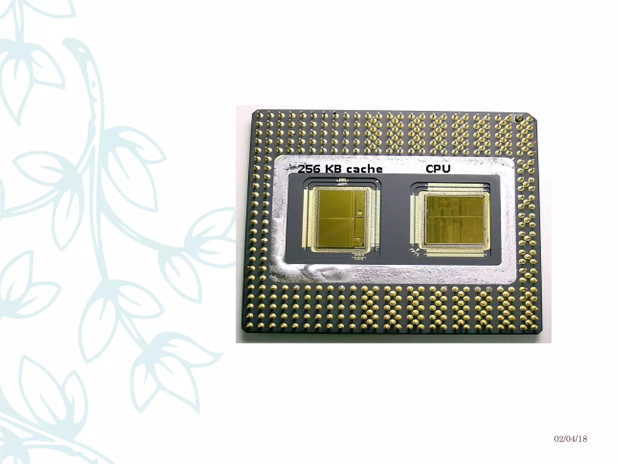
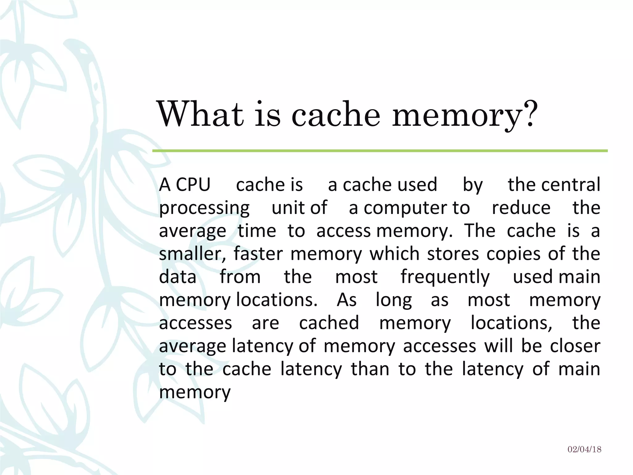
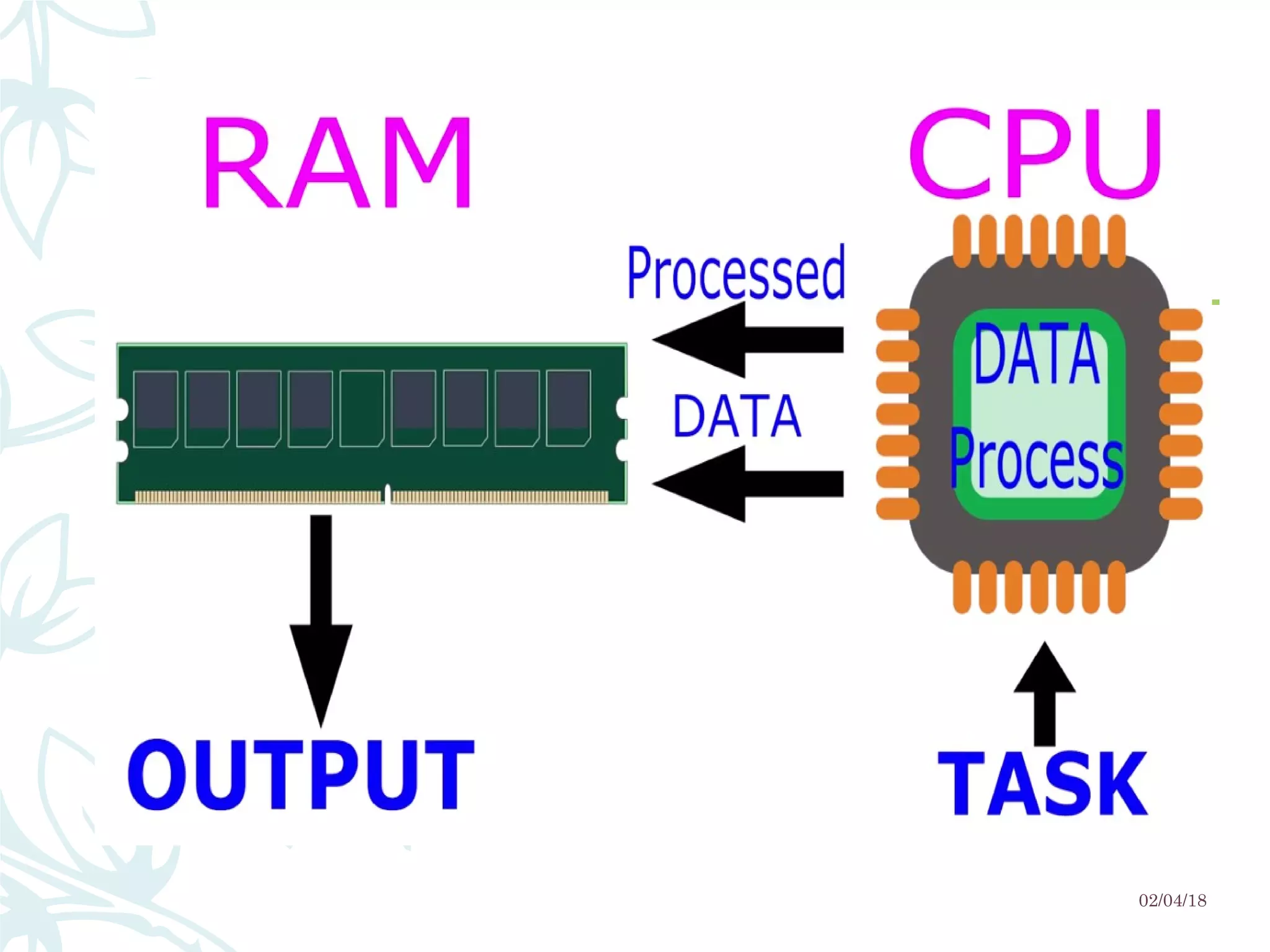
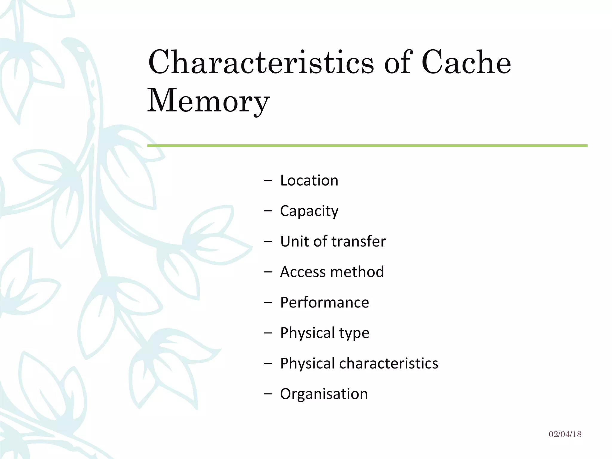
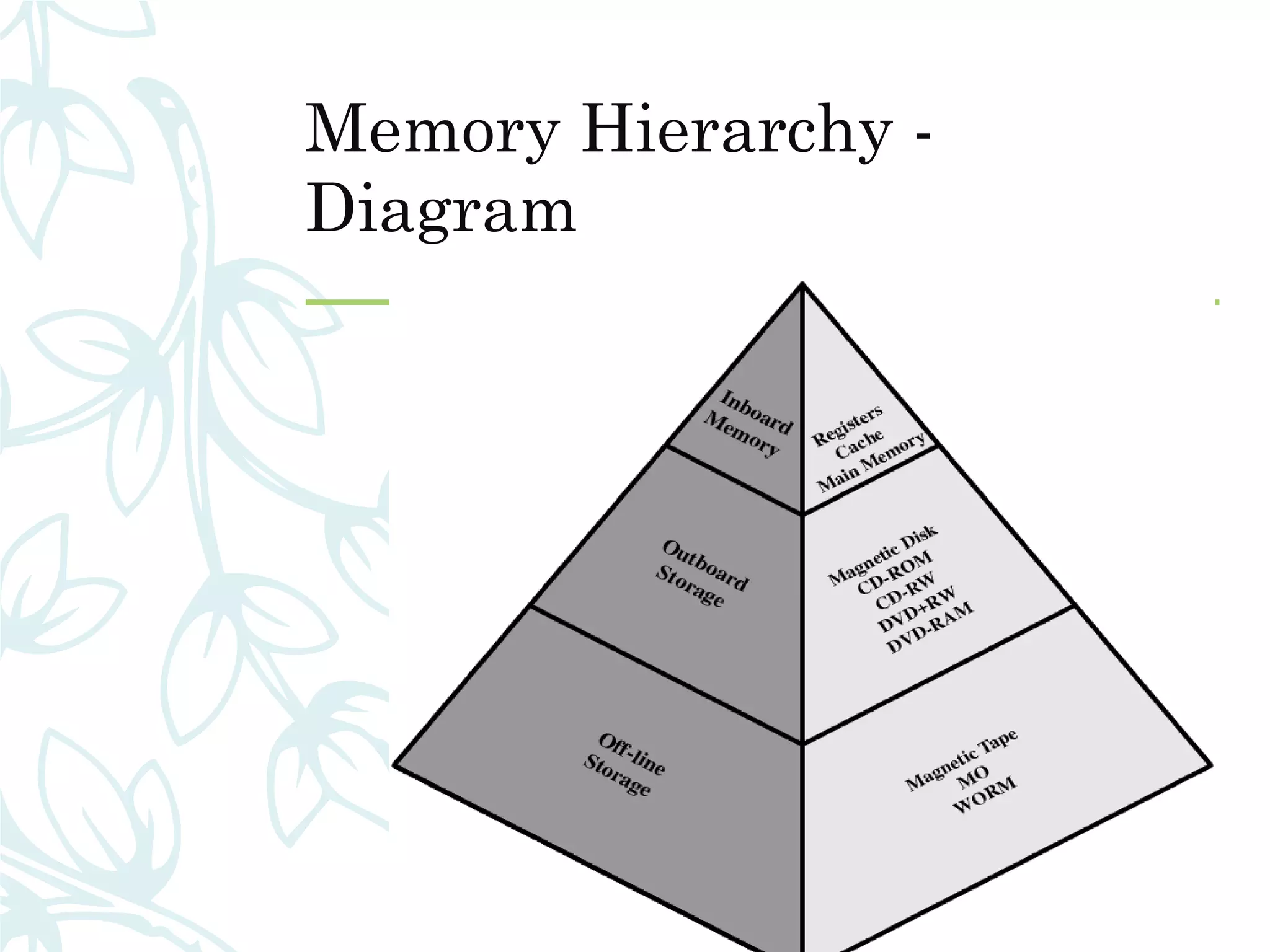
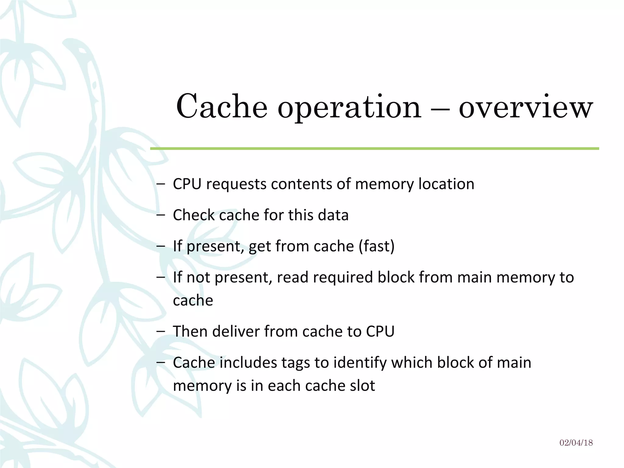
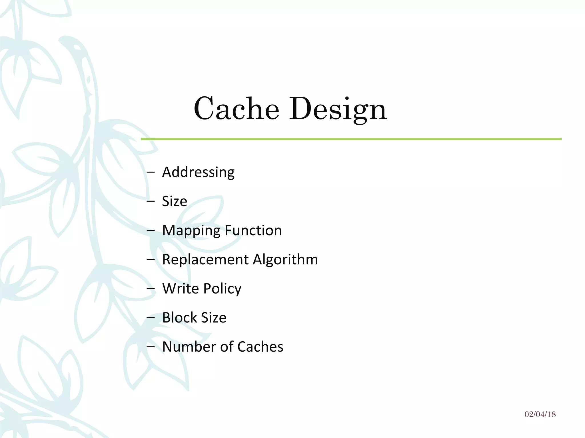
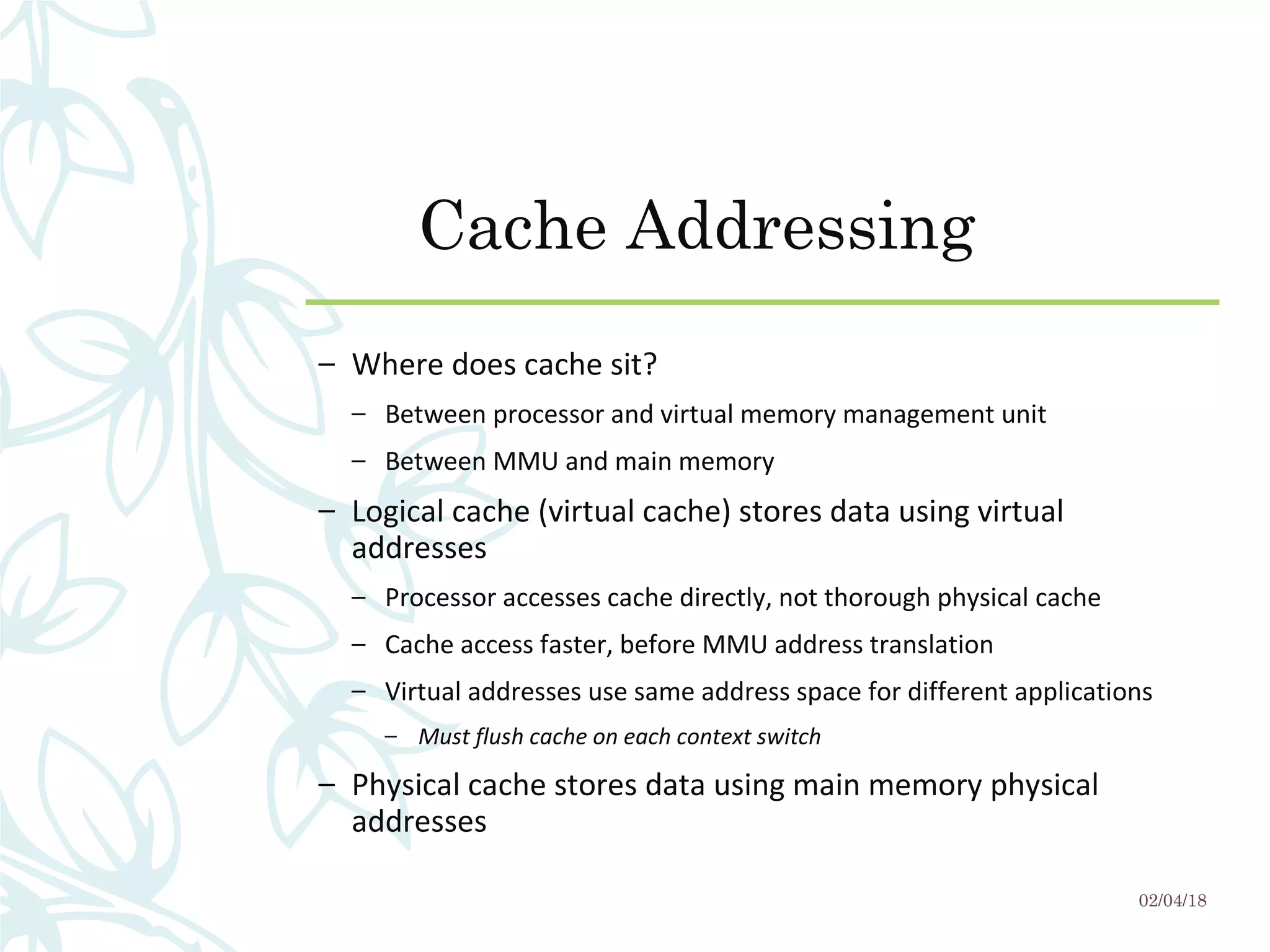
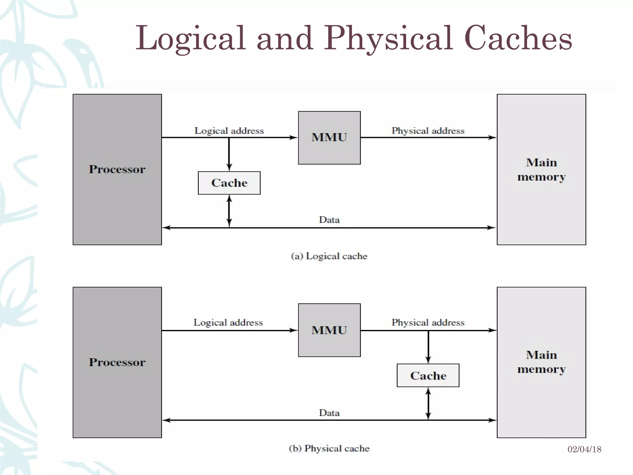
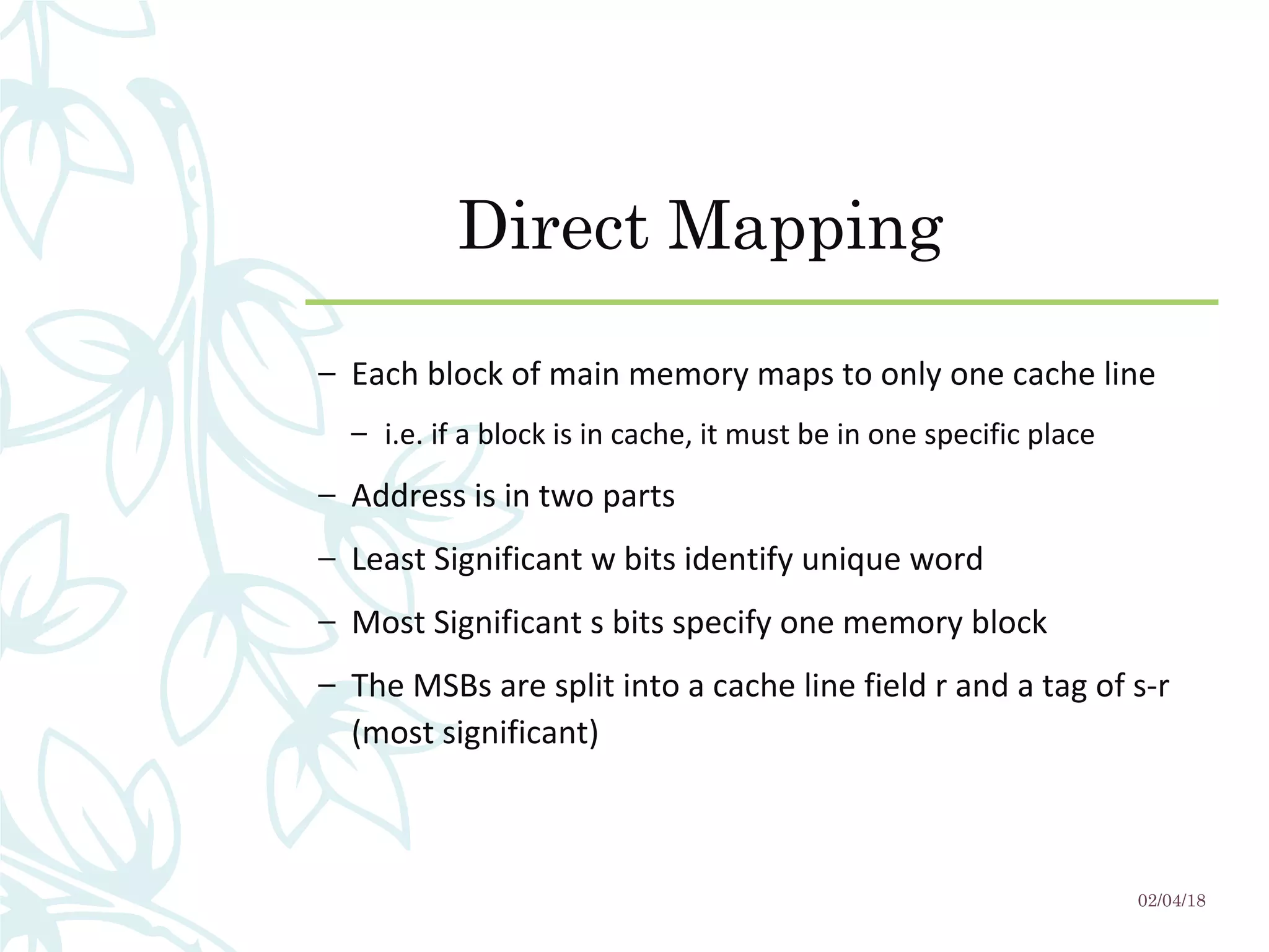
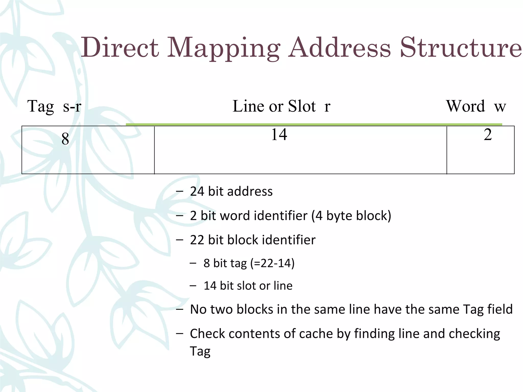
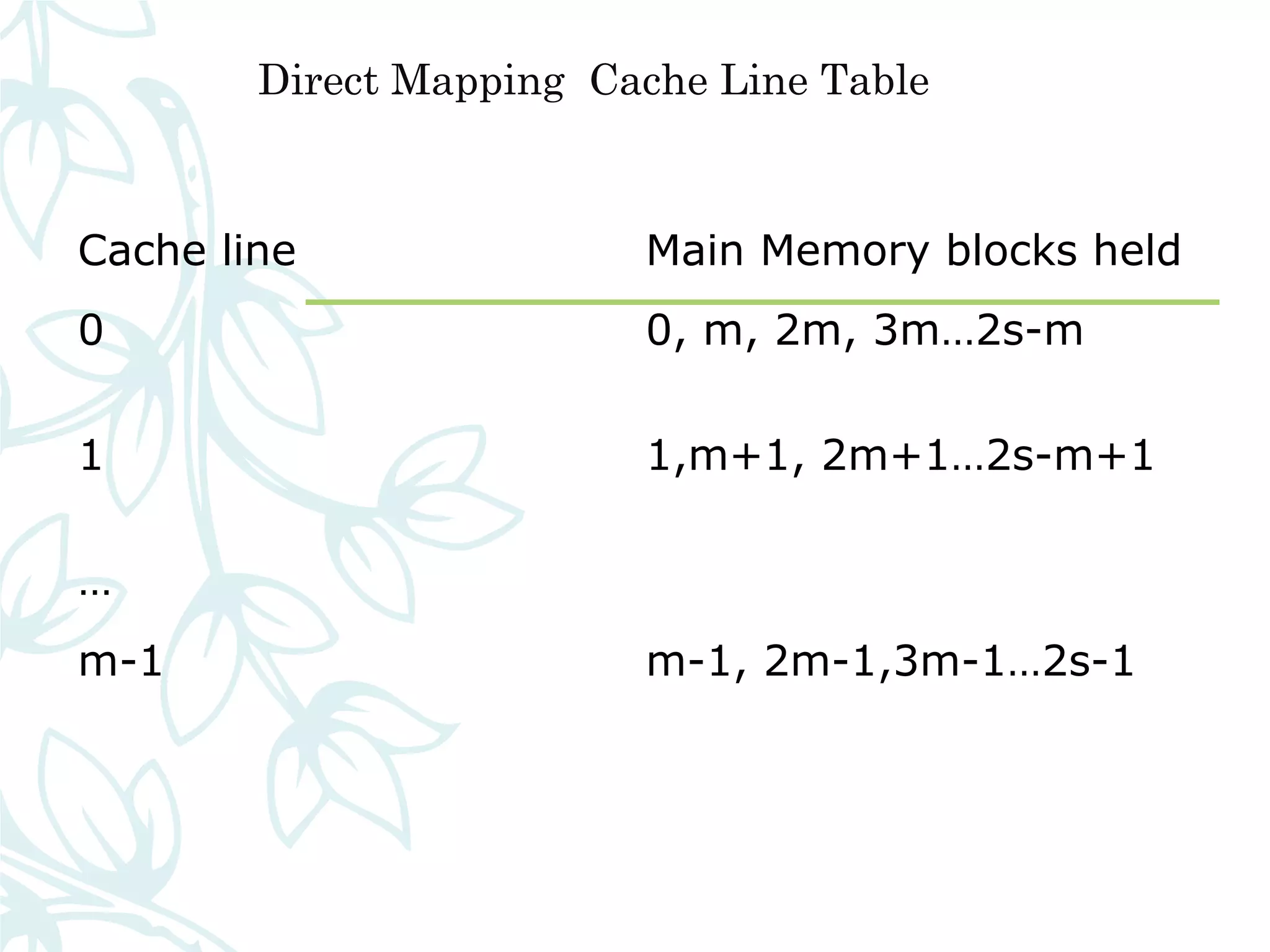
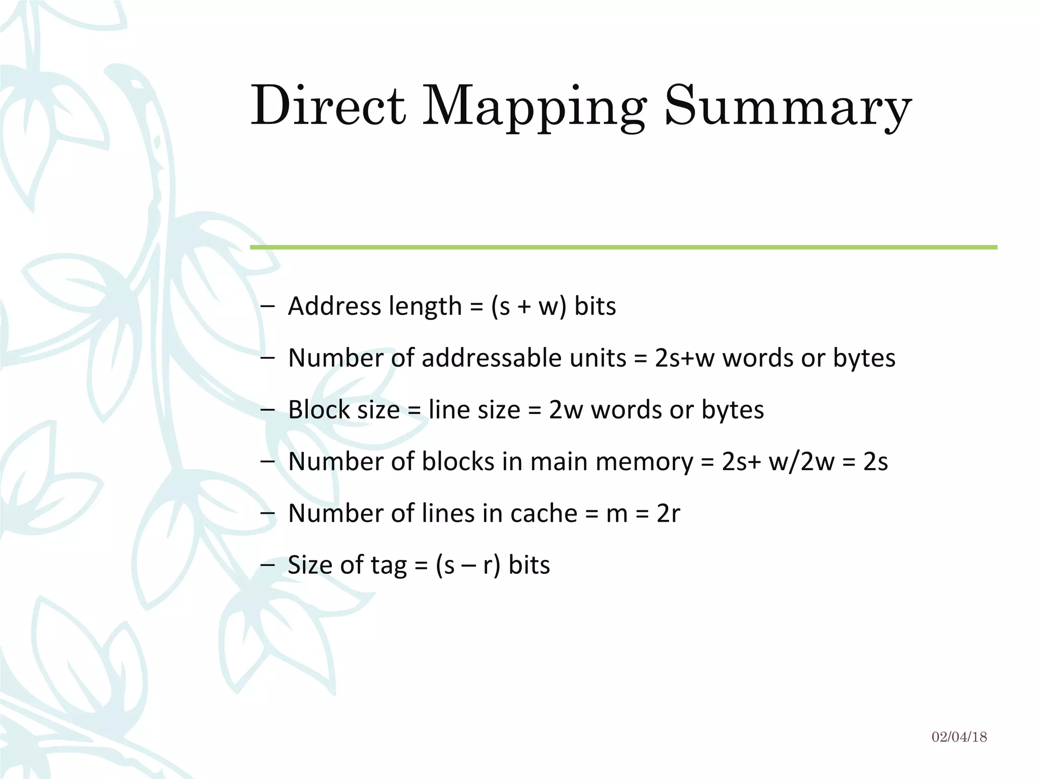
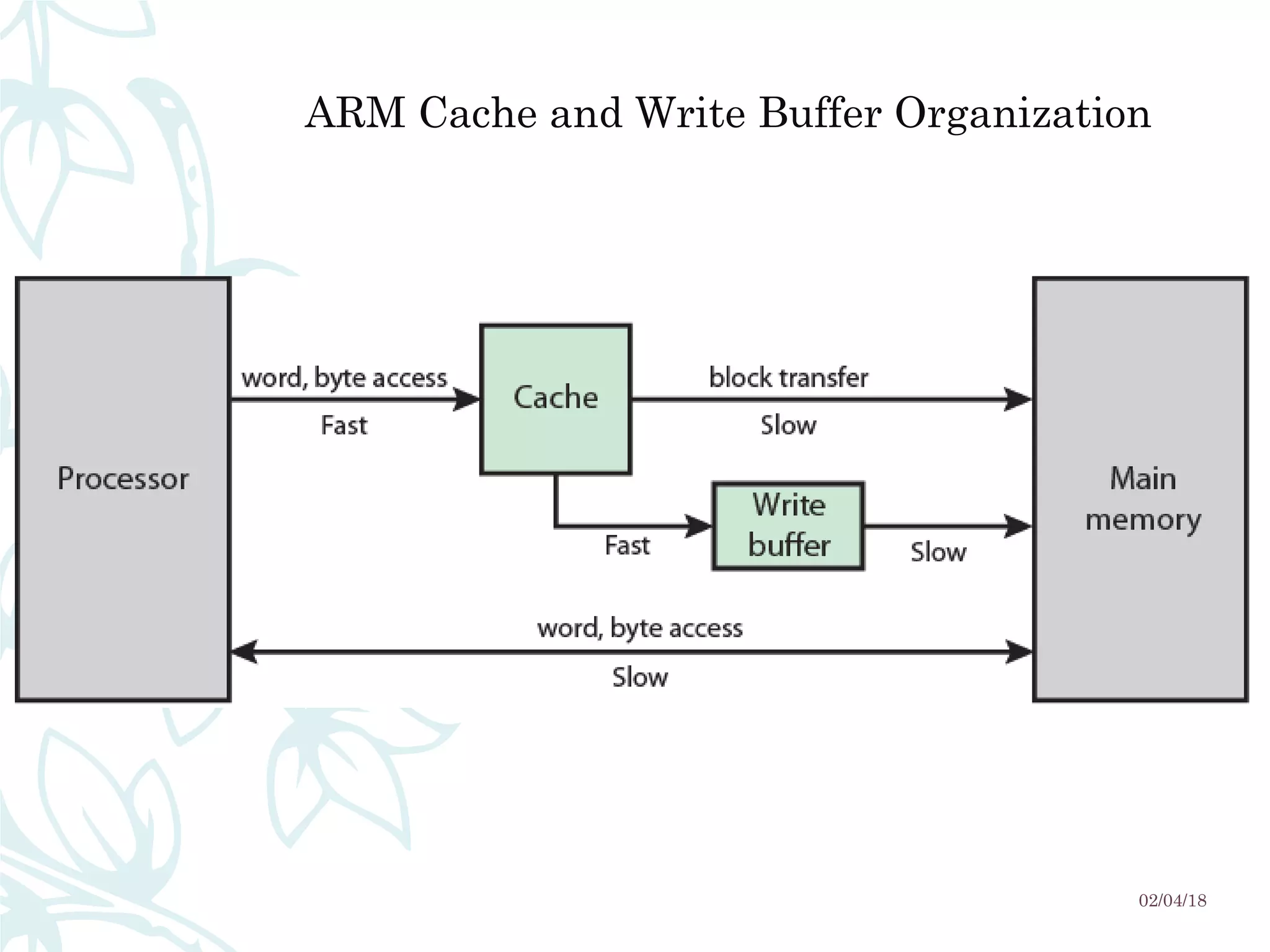
CaChe MeMoryCaChe MeMory
Md. Foysal Mahmud
Roll: 14CSE028
Dpt. Of CSE.
University of
Barisal
02/04/18
What is cache memory?
A CPU  cache is  a cache used  by  the central 
processing  unit of  a computer to  reduce  the 
average  time  to  access memory.  The  cache  is  a 
smaller, faster memory which stores copies of the 
data  from  the  most  frequently  used main 
memory locations.  As  long  as  most  memory 
accesses  are  cached  memory  locations,  the 
average latency of memory accesses will be closer 
to  the  cache  latency  than  to  the  latency  of  main 
memory 
02/04/18
What is Cache Memory?
– Cache memory is used in order to achieve higher performance 
of CPU by allowing the CPU to access data at faster speed.
– It is placed closest to the processor in the computer assembly.
– It is way too costly.
– It is also a type of memory but keeping in mind the cost factor it 
cannot be used as a primary memory.
02/04/18
02/04/18
02/04/18
Characteristics of Cache
Memory
– Location
– Capacity
– Unit of transfer
– Access method
– Performance
– Physical type
– Physical characteristics
– Organisation
02/04/18
Location
– CPU
– Internal
– External
02/04/18
Capacity
– Word size
– The natural unit of organisation
– For example, the
– CRAY C90 (an older model CRAY supercomputer) has a 
64-bit word length but uses a 46-bit integer 
representation. 
– The Intel x86 architecture has a wide variety of 
instruction lengths, expressed as multiples of bytes, 
and a word size of 32 bits.
– Number of words
– or Bytes 02/04/18
Unit of Transfer
– Internal
– Usually governed by data bus width
– External
– Usually a block which is much larger than a word
– Addressable unit
– Smallest location which can be uniquely addressed
– Word internally
– Cluster on M$ disks
02/04/18
Access Methods (1)
Sequential
Start at the beginning and read through in order
Access time depends on location of data and previous location
e.g. tape
Direct
Individual blocks have unique address
Access is by jumping to vicinity plus sequential search
Access time depends on location and previous location
e.g. disk
02/04/18
Access Methods (2)
Random
Individual addresses identify locations exactly
Access time is independent of location or previous access
e.g. RAM
Associative
Data is located by a comparison with contents of a portion of
the store
Access time is independent of location or previous access
e.g. cache
02/04/18
Memory Hierarchy
– Registers
– In CPU
– Internal or Main memory
– May include one or more levels of cache
– “RAM”
– External memory
– Backing store
02/04/18
Memory Hierarchy -
Diagram
02/04/18
Performance
– Access time
– Time between presenting the address and getting the valid
data
– Memory Cycle time
– Time may be required for the memory to “recover” before next
access
– Cycle time is access + recovery
– Transfer Rate
– Rate at which data can be moved
02/04/18
Cache
– Small amount of fast memory
– Sits between normal main memory and CPU
– May be located on CPU chip or module
02/04/18
02/04/18
02/04/18
Cache operation – overview
– CPU requests contents of memory location
– Check cache for this data
– If present, get from cache (fast)
– If not present, read required block from main memory to
cache
– Then deliver from cache to CPU
– Cache includes tags to identify which block of main
memory is in each cache slot
02/04/18
Cache Read Operation - Flowchart
02/04/18
Cache Design
– Addressing
– Size
– Mapping Function
– Replacement Algorithm
– Write Policy
– Block Size
– Number of Caches
02/04/18
Cache Addressing
– Where does cache sit?
– Between processor and virtual memory management unit
– Between MMU and main memory
– Logical cache (virtual cache) stores data using virtual
addresses
– Processor accesses cache directly, not thorough physical cache
– Cache access faster, before MMU address translation
– Virtual addresses use same address space for different applications
– Must flush cache on each context switch
– Physical cache stores data using main memory physical
addresses
02/04/18
Size does matter
– Cost
– More cache is expensive
– Speed
– More cache is faster (up to a point)
– Checking cache for data takes time
02/04/18
Typical Cache Organization
02/04/18
Logical and Physical Caches
02/04/18
Comparison of Cache Sizes
02/04/18
Processor Type
Year of
Introduction
L1 cache L2 cache L3 cache
IBM 360/85 Mainframe 1968 16 to 32 KB — —
PDP-11/70 Minicomputer 1975 1 KB — —
VAX 11/780 Minicomputer 1978 16 KB — —
IBM 3033 Mainframe 1978 64 KB — —
IBM 3090 Mainframe 1985 128 to 256 KB — —
Intel 80486 PC 1989 8 KB — —
Pentium PC 1993 8 KB/8 KB 256 to 512 KB —
PowerPC 601 PC 1993 32 KB — —
PowerPC 620 PC 1996 32 KB/32 KB — —
PowerPC G4 PC/server 1999 32 KB/32 KB 256 KB to 1 MB 2 MB
IBM S/390 G4 Mainframe 1997 32 KB 256 KB 2 MB
IBM S/390 G6 Mainframe 1999 256 KB 8 MB —
Pentium 4 PC/server 2000 8 KB/8 KB 256 KB —
IBM SP
High-end server/
supercomputer
2000 64 KB/32 KB 8 MB —
CRAY MTAb Supercomputer 2000 8 KB 2 MB —
Itanium PC/server 2001 16 KB/16 KB 96 KB 4 MB
SGI Origin 2001 High-end server 2001 32 KB/32 KB 4 MB —
Itanium 2 PC/server 2002 32 KB 256 KB 6 MB
IBM POWER5 High-end server 2003 64 KB 1.9 MB 36 MB
CRAY XD-1 Supercomputer 2004 64 KB/64 KB 1MB —
Mapping Function
– Cache of 64kByte
– Cache block of 4 bytes
– i.e. cache is 16k (214
) lines of 4 bytes
– 16MBytes main memory
– 24 bit address
– (224
=16M)
02/04/18
Direct Mapping
– Each block of main memory maps to only one cache line
– i.e. if a block is in cache, it must be in one specific place
– Address is in two parts
– Least Significant w bits identify unique word
– Most Significant s bits specify one memory block
– The MSBs are split into a cache line field r and a tag of s-r
(most significant)
02/04/18
Direct Mapping Address Structure
– 24 bit address
– 2 bit word identifier (4 byte block)
– 22 bit block identifier
– 8 bit tag (=22-14)
– 14 bit slot or line
– No two blocks in the same line have the same Tag field
– Check contents of cache by finding line and checking
Tag
Tag s-r Line or Slot r Word w
8 14 2
02/04/18
Direct Mapping from Cache to Main Memory
02/04/18
Direct Mapping Cache Line Table
Cache line Main Memory blocks held
0 0, m, 2m, 3m…2s-m
1 1,m+1, 2m+1…2s-m+1
…
m-1 m-1, 2m-1,3m-1…2s-1
Direct Mapping Cache Organization
02/04/18
Direct Mapping Summary
– Address length = (s + w) bits
– Number of addressable units = 2s+w words or bytes
– Block size = line size = 2w words or bytes
– Number of blocks in main memory = 2s+ w/2w = 2s
– Number of lines in cache = m = 2r
– Size of tag = (s – r) bits
02/04/18
Associative Mapping
– A main memory block can load into any line of cache
– Memory address is interpreted as tag and word
– Tag uniquely identifies block of memory
– Every line’s tag is examined for a match
– Cache searching gets expensive
02/04/18
Associative Mapping from
Cache to Main Memory
02/04/18
Fully Associative Cache
Organization
02/04/18
Tag 22 bit
Word
2 bit
Associative Mapping
Address Structure
– 22 bit tag stored with each 32 bit block of data
– Compare tag field with tag entry in cache to check for hit
– Least significant 2 bits of address identify which 16 bit word is
required from 32 bit data block
– e.g.
– Address Tag Data Cache line
– FFFFFC FFFFFC 24682468 3FFF
02/04/18
Associative Mapping
Summary
– Address length = (s + w) bits
– Number of addressable units = 2s+w words or bytes
– Block size = line size = 2w words or bytes
– Number of blocks in main memory = 2s+ w/2w = 2s
– Number of lines in cache = undetermined
– Size of tag = s bits
02/04/18
Replacement Algorithms (1)
Direct mapping
– No choice
– Each block only maps to one line
– Replace that line
02/04/18
Replacement Algorithms (2)
Associative & Set Associative
– Hardware implemented algorithm (speed)
– Least Recently used (LRU)
– e.g. in 2 way set associative
– Which of the 2 block is lru?
– First in first out (FIFO)
– replace block that has been in cache longest
– Least frequently used
– replace block which has had fewest hits
– Random
02/04/18
ARM Cache Organization
– Small FIFO write buffer
– Enhances memory write performance
– Between cache and main memory
– Small c.f. cache
– Data put in write buffer at processor clock speed
– Processor continues execution
– External write in parallel until empty
– If buffer full, processor stalls
– Data in write buffer not available until written
– So keep buffer small
02/04/18
ARM Cache and Write Buffer Organization
02/04/18

Cache memory by Foysal

  • 1.
    CaChe MeMoryCaChe MeMory Md.Foysal Mahmud Roll: 14CSE028 Dpt. Of CSE. University of Barisal
  • 2.
  • 3.
    What is cachememory? A CPU  cache is  a cache used  by  the central  processing  unit of  a computer to  reduce  the  average  time  to  access memory.  The  cache  is  a  smaller, faster memory which stores copies of the  data  from  the  most  frequently  used main  memory locations.  As  long  as  most  memory  accesses  are  cached  memory  locations,  the  average latency of memory accesses will be closer  to  the  cache  latency  than  to  the  latency  of  main  memory  02/04/18
  • 4.
    What is CacheMemory? – Cache memory is used in order to achieve higher performance  of CPU by allowing the CPU to access data at faster speed. – It is placed closest to the processor in the computer assembly. – It is way too costly. – It is also a type of memory but keeping in mind the cost factor it  cannot be used as a primary memory. 02/04/18
  • 5.
  • 6.
  • 7.
    Characteristics of Cache Memory –Location – Capacity – Unit of transfer – Access method – Performance – Physical type – Physical characteristics – Organisation 02/04/18
  • 8.
  • 9.
    Capacity – Word size – The natural unit of organisation –For example, the – CRAY C90 (an older model CRAY supercomputer) has a  64-bit word length but uses a 46-bit integer  representation.  – The Intel x86 architecture has a wide variety of  instruction lengths, expressed as multiples of bytes,  and a word size of 32 bits. – Number of words – or Bytes 02/04/18
  • 10.
    Unit of Transfer –Internal – Usually governed by data bus width – External – Usually a block which is much larger than a word – Addressable unit – Smallest location which can be uniquely addressed – Word internally – Cluster on M$ disks 02/04/18
  • 11.
  • 12.
    Access Methods (2) Random Individualaddresses identify locations exactly Access time is independent of location or previous access e.g. RAM Associative Data is located by a comparison with contents of a portion of the store Access time is independent of location or previous access e.g. cache 02/04/18
  • 13.
    Memory Hierarchy – Registers –In CPU – Internal or Main memory – May include one or more levels of cache – “RAM” – External memory – Backing store 02/04/18
  • 14.
  • 15.
    Performance – Access time –Time between presenting the address and getting the valid data – Memory Cycle time – Time may be required for the memory to “recover” before next access – Cycle time is access + recovery – Transfer Rate – Rate at which data can be moved 02/04/18
  • 16.
    Cache – Small amountof fast memory – Sits between normal main memory and CPU – May be located on CPU chip or module 02/04/18
  • 17.
  • 18.
  • 19.
    Cache operation –overview – CPU requests contents of memory location – Check cache for this data – If present, get from cache (fast) – If not present, read required block from main memory to cache – Then deliver from cache to CPU – Cache includes tags to identify which block of main memory is in each cache slot 02/04/18
  • 20.
    Cache Read Operation- Flowchart 02/04/18
  • 21.
    Cache Design – Addressing –Size – Mapping Function – Replacement Algorithm – Write Policy – Block Size – Number of Caches 02/04/18
  • 22.
    Cache Addressing – Wheredoes cache sit? – Between processor and virtual memory management unit – Between MMU and main memory – Logical cache (virtual cache) stores data using virtual addresses – Processor accesses cache directly, not thorough physical cache – Cache access faster, before MMU address translation – Virtual addresses use same address space for different applications – Must flush cache on each context switch – Physical cache stores data using main memory physical addresses 02/04/18
  • 23.
    Size does matter –Cost – More cache is expensive – Speed – More cache is faster (up to a point) – Checking cache for data takes time 02/04/18
  • 24.
  • 25.
    Logical and PhysicalCaches 02/04/18
  • 26.
    Comparison of CacheSizes 02/04/18 Processor Type Year of Introduction L1 cache L2 cache L3 cache IBM 360/85 Mainframe 1968 16 to 32 KB — — PDP-11/70 Minicomputer 1975 1 KB — — VAX 11/780 Minicomputer 1978 16 KB — — IBM 3033 Mainframe 1978 64 KB — — IBM 3090 Mainframe 1985 128 to 256 KB — — Intel 80486 PC 1989 8 KB — — Pentium PC 1993 8 KB/8 KB 256 to 512 KB — PowerPC 601 PC 1993 32 KB — — PowerPC 620 PC 1996 32 KB/32 KB — — PowerPC G4 PC/server 1999 32 KB/32 KB 256 KB to 1 MB 2 MB IBM S/390 G4 Mainframe 1997 32 KB 256 KB 2 MB IBM S/390 G6 Mainframe 1999 256 KB 8 MB — Pentium 4 PC/server 2000 8 KB/8 KB 256 KB — IBM SP High-end server/ supercomputer 2000 64 KB/32 KB 8 MB — CRAY MTAb Supercomputer 2000 8 KB 2 MB — Itanium PC/server 2001 16 KB/16 KB 96 KB 4 MB SGI Origin 2001 High-end server 2001 32 KB/32 KB 4 MB — Itanium 2 PC/server 2002 32 KB 256 KB 6 MB IBM POWER5 High-end server 2003 64 KB 1.9 MB 36 MB CRAY XD-1 Supercomputer 2004 64 KB/64 KB 1MB —
  • 27.
    Mapping Function – Cacheof 64kByte – Cache block of 4 bytes – i.e. cache is 16k (214 ) lines of 4 bytes – 16MBytes main memory – 24 bit address – (224 =16M) 02/04/18
  • 28.
    Direct Mapping – Eachblock of main memory maps to only one cache line – i.e. if a block is in cache, it must be in one specific place – Address is in two parts – Least Significant w bits identify unique word – Most Significant s bits specify one memory block – The MSBs are split into a cache line field r and a tag of s-r (most significant) 02/04/18
  • 29.
    Direct Mapping AddressStructure – 24 bit address – 2 bit word identifier (4 byte block) – 22 bit block identifier – 8 bit tag (=22-14) – 14 bit slot or line – No two blocks in the same line have the same Tag field – Check contents of cache by finding line and checking Tag Tag s-r Line or Slot r Word w 8 14 2
  • 30.
  • 31.
    Direct Mapping fromCache to Main Memory 02/04/18
  • 32.
    Direct Mapping CacheLine Table Cache line Main Memory blocks held 0 0, m, 2m, 3m…2s-m 1 1,m+1, 2m+1…2s-m+1 … m-1 m-1, 2m-1,3m-1…2s-1
  • 33.
    Direct Mapping CacheOrganization 02/04/18
  • 34.
    Direct Mapping Summary –Address length = (s + w) bits – Number of addressable units = 2s+w words or bytes – Block size = line size = 2w words or bytes – Number of blocks in main memory = 2s+ w/2w = 2s – Number of lines in cache = m = 2r – Size of tag = (s – r) bits 02/04/18
  • 35.
    Associative Mapping – Amain memory block can load into any line of cache – Memory address is interpreted as tag and word – Tag uniquely identifies block of memory – Every line’s tag is examined for a match – Cache searching gets expensive 02/04/18
  • 36.
    Associative Mapping from Cacheto Main Memory 02/04/18
  • 37.
  • 38.
    Tag 22 bit Word 2bit Associative Mapping Address Structure – 22 bit tag stored with each 32 bit block of data – Compare tag field with tag entry in cache to check for hit – Least significant 2 bits of address identify which 16 bit word is required from 32 bit data block – e.g. – Address Tag Data Cache line – FFFFFC FFFFFC 24682468 3FFF 02/04/18
  • 39.
    Associative Mapping Summary – Addresslength = (s + w) bits – Number of addressable units = 2s+w words or bytes – Block size = line size = 2w words or bytes – Number of blocks in main memory = 2s+ w/2w = 2s – Number of lines in cache = undetermined – Size of tag = s bits 02/04/18
  • 40.
    Replacement Algorithms (1) Directmapping – No choice – Each block only maps to one line – Replace that line 02/04/18
  • 41.
    Replacement Algorithms (2) Associative& Set Associative – Hardware implemented algorithm (speed) – Least Recently used (LRU) – e.g. in 2 way set associative – Which of the 2 block is lru? – First in first out (FIFO) – replace block that has been in cache longest – Least frequently used – replace block which has had fewest hits – Random 02/04/18
  • 42.
    ARM Cache Organization –Small FIFO write buffer – Enhances memory write performance – Between cache and main memory – Small c.f. cache – Data put in write buffer at processor clock speed – Processor continues execution – External write in parallel until empty – If buffer full, processor stalls – Data in write buffer not available until written – So keep buffer small 02/04/18
  • 43.
    ARM Cache andWrite Buffer Organization 02/04/18