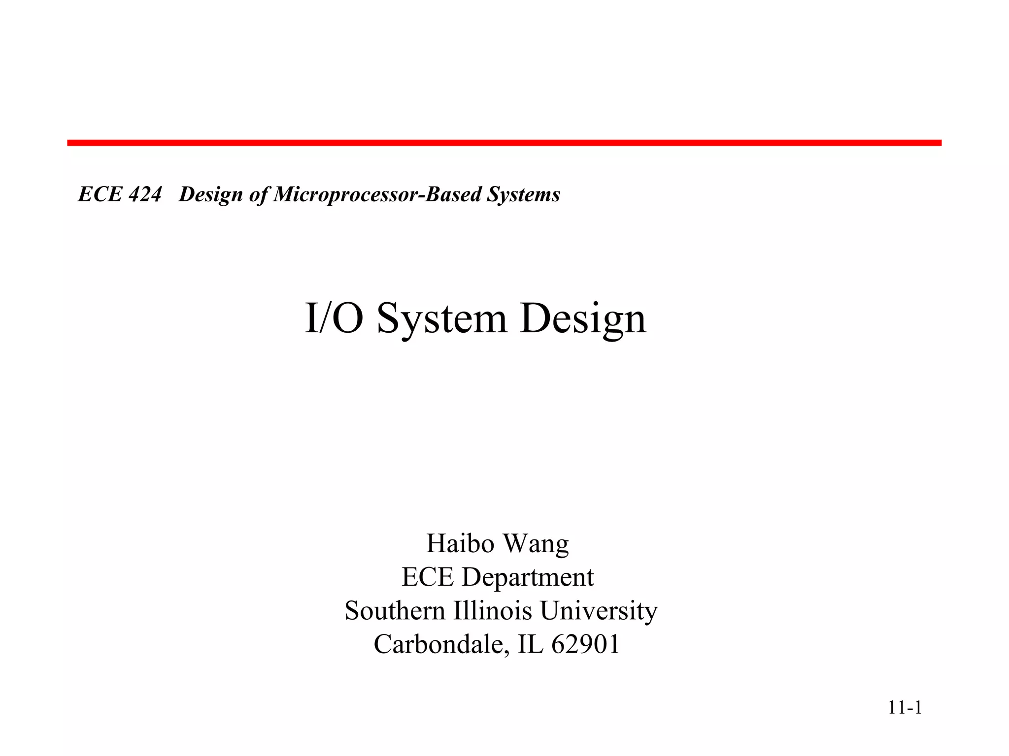
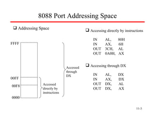
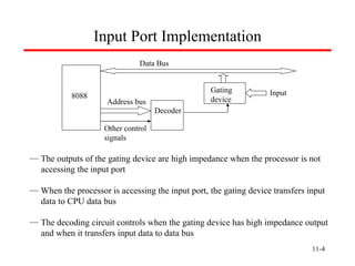
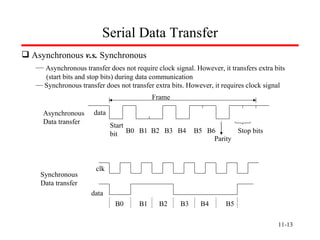
The document discusses the input/output system of the 8088 microprocessor. It describes the 8088's I/O addressing space and port addressing methods. It provides examples of implementing input and output ports using decoding circuits and input/output gating devices. It also discusses the 8255 Programmable Peripheral Interface chip and 8251 Universal Synchronous/Asynchronous Receiver/Transmitter, providing details on their programming and interfacing with the 8088 microprocessor.
![11- Overview of 8088 I/O System 65,536 possible I/O ports Data transfer between ports and the processor is over data bus 8088 uses address bus A[15:0] to locate an I/O port AL (or AX) is the processor register that takes input data (or provide output data) I/O I/O I/O Data bus Address bus A[15:0] AL AX 8088](https://image.slidesharecdn.com/io2-090920123656-phpapp02/85/Io-2-2-320.jpg)
![11- 8255 Programmable Peripheral Interface Data bus 8088 D[7:0] A0 A1 RD WR RESET CS Control port PA[7:0] PB[7:0] PC[7:0] A7 A6 A5 A4 A3 A2 IO/M A1 A0 Port 0 0 0 1 0 1 1 PA PB PC Control](https://image.slidesharecdn.com/io2-090920123656-phpapp02/85/Io-2-9-320.jpg)
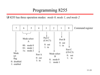
![11- Programming 8255 Mode 0: Ports A, B, and C can be individually programmed as input or output ports Port C is divided into two 4-bit ports which are independent from each other Mode 1: Ports A and B are programmed as input or output ports Port C is used for handshaking PA[7:0] STB A IBF A INTR A PC3 PC5 PC4 PB[7:0] STB B IBF B INTR B PC0 PC1 PC2 PC6, 7 8255 PA[7:0] OBF A ACK A INTR A PC3 PC6 PC7 PB[7:0] OBF B ACK B INTR B PC0 PC1 PC2 PC4, 5 8255](https://image.slidesharecdn.com/io2-090920123656-phpapp02/85/Io-2-11-320.jpg)
![11- Programming 8255 Mode 2: Port A is programmed to be bi-directional Port C is for handshaking Port B can be either input or output in mode 0 or mode 1 Can you design a decoder for an 8255 chip such that its base address is 40H? Write the instructions that set 8255 into mode 0, port A as input, port B as output, PC0-PC3 as input, PC4-PC7 as output ? PA[7:0] OBF A ACK A INTR A PC4 PC6 PC7 STB A IBF A PC0 PC3 PC5 8255 PC0 PC0 PB[7:0] In Out In Out In Out Mode 0 STB B OBF B IBF B ACK B INTR B INTR B Mode 1](https://image.slidesharecdn.com/io2-090920123656-phpapp02/85/Io-2-12-320.jpg)
![11- 8251 USART Interface A7 A6 A5 A4 A3 A2 A1 IO/M D[7:0] RD RD WR WR A0 C/D CLK CLK TxC RxC TxD RxD 8251 RS232](https://image.slidesharecdn.com/io2-090920123656-phpapp02/85/Io-2-14-320.jpg)