Downloaded 219 times

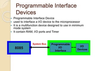


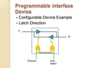
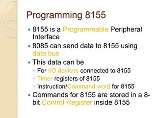


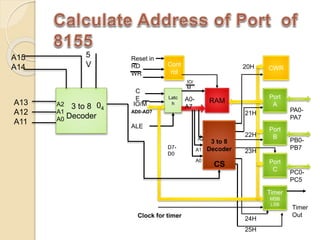

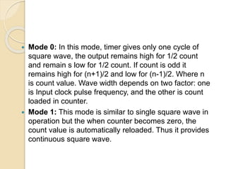

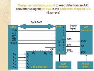
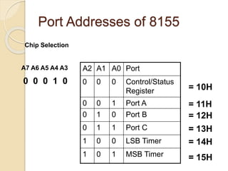
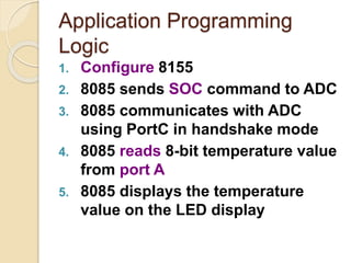

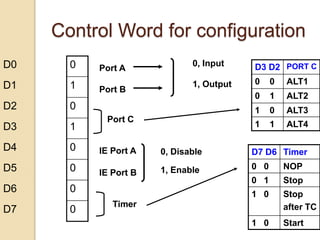
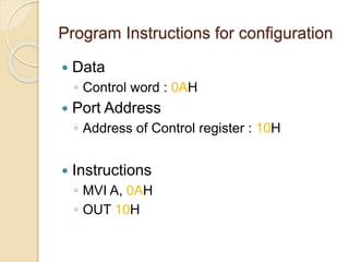
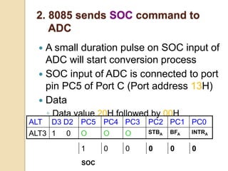
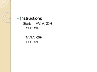


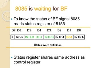
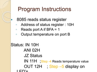
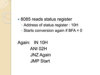
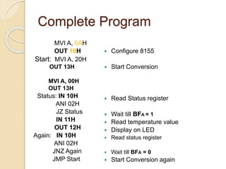
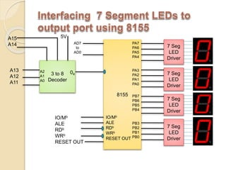


The document discusses the 8155 Programmable Peripheral Interface chip. It can be used as an interface between a microprocessor and I/O devices. The 8155 contains RAM, I/O ports, and a timer. It has ports A, B, and C that can be configured as input or output. The timer can operate in different modes. Programming the 8155 involves writing control words to its control register to configure the ports and timer. An example application shows how an 8155 can be used to interface an ADC and read temperature values using handshaking between the ADC and 8155 ports.