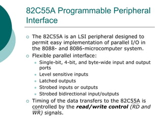
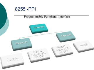
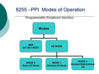
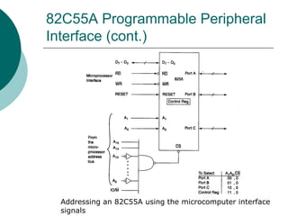
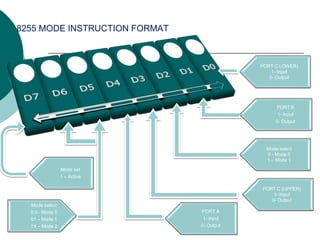
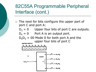
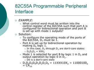
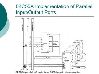
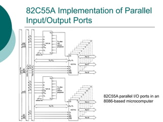
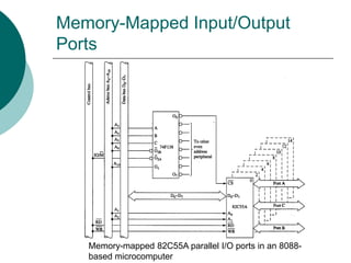
The 82C55A is an LSI peripheral designed to permit easy implementation of parallel I/O in 8088- and 8086-based microcomputer systems. It contains three 8-bit ports that can each be configured independently for input, output, or bidirectional operation. The timing and configuration of data transfers to and from the ports is controlled by an 8-bit internal register that can select different operating modes.
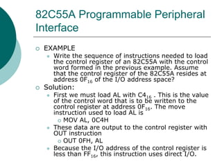
![Memory-Mapped Input/Output
Ports
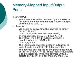
From the circuit diagram, the memory address of
the control register for PPI 0 is found to be
000000000100000001102 = 0040616
Since PPI 0 is memory mapped, the following
move instructions can be used to initialized the
control register:
MOV AX, 0 ; Create data segment at 00000H
MOV DS, AX
MOV AL, 8BH ; Load AL with control byte
MOV [406H], AL ; Write control byte to PPI 0
control register](https://image.slidesharecdn.com/8255-221125142702-d04fda12/85/8255-ppt-42-320.jpg)
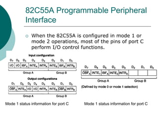
![Memory-Mapped Input/Output
Ports
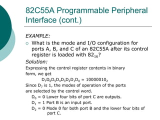
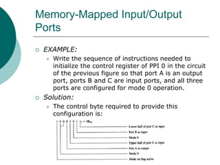
EXAMPLE:
Assume that PPI 0 in the previous figure is configured
as described in the previous example. Write a program
that will input the contents of ports B and C, AND
them together, and output the results to port A.
Solution:
The addresses of the three I/O ports on PPI 0 are:
Port A = 0040016 Port B = 0040216 Port C =
0040416
Now we set up a data segment at 0000016 and the
program is:
AND AX, 0 ; Create data segment at 00000H
MOV DS, AX
MOV BL, [402H] ; Read port B
MOV AL, [404H] ; Read port C
AND AL, BL ; AND data at port B and C
MOV [400H], AL ; Write to port A](https://image.slidesharecdn.com/8255-221125142702-d04fda12/85/8255-ppt-43-320.jpg)