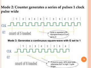
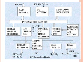
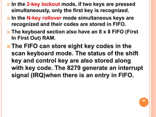
This document provides an overview of Unit III - I/O Interfacing in a syllabus. It discusses various topics related to interfacing memory and I/O devices, including parallel communication interfaces like the 8255 PPI chip, serial communication interfaces like the 8251 USART, and analog interfaces such as A/D converters, D/A converters, and timers. It also lists some case studies and applications that will be covered, including traffic light control, LED displays, LCD displays, keyboard/display interfaces, and alarm controllers.


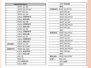
![8086 ALP:
1100: START: MOV BX, 1200H
MOV CX, 0008H
MOV AL,[BX]
MOV DX, CONTROL PORT
OUT DX, AL
INC BX
NEXT: MOV AL,[BX]
MOV DX, PORT A
OUT DX,AL
CALL DELAY
INC BX
LOOP NEXT
JMP START
DELAY: PUSH CX
MOV CX,0005H
REPEAT: MOV DX,0FFFFH
LOOP2: DEC DX
JNZ LOOP2
LOOP REPEAT
POP CX
RET
145](https://image.slidesharecdn.com/mpmcunit-iii-240316061641-3fcf2c41/85/MicroProcessors-and-MicroControllersUnit3-145-320.jpg)