Downloaded 38 times
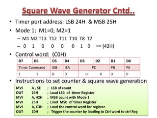
![• M2, M1: mode bits:
– 00: Single square wave of wavelength TC/2 (TC/2,TC/2
if TC even; [TC+1/2],[TC-1/2] if TC odd)
– 01: Square waves of wavelength TC (TC/2,TC/2 if TC
even; [TC+1/2],[TC-1/2] if TC odd)
– 10: Single pulse on the TC'th clock pulse
– 11: Single pulse on every TC'th clock pulse.
MSB
M2 M1 T13 T12 T11 T10 T9 T8
LSB
T7 T6 T5 T4 T3 T2 T1 T0](https://image.slidesharecdn.com/lec12-150215030520-conversion-gate01/85/Lec12-11-320.jpg)
![– 00: Single square wave of wavelength TC/2
(TC/2,TC/2 if TC even; [TC+1/2],[TC-1/2] if TC odd)
– 01: Square waves of wavelength TC (TC/2,TC/2 if TC
even; [TC+1/2],[TC-1/2] if TC odd)
– 10: Single pulse on the TC'th clock pulse
– 11: Single pulse on every TC'th clock pulse.
CLK
WR
Mode 00
Mode 01
Mode 10
Mode 11
N/2 N/2
N/2 N/2 N/2N/2
N
N N](https://image.slidesharecdn.com/lec12-150215030520-conversion-gate01/85/Lec12-12-320.jpg)


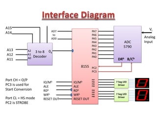
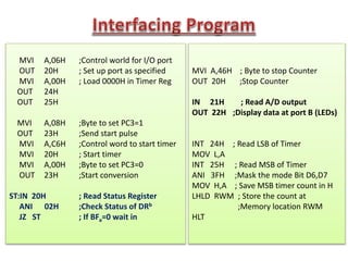


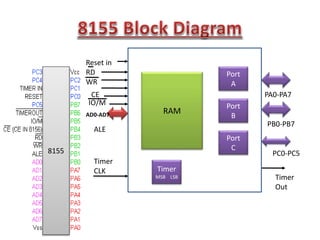
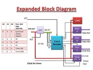
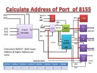
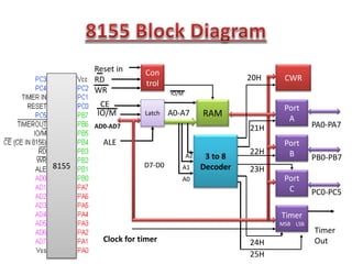
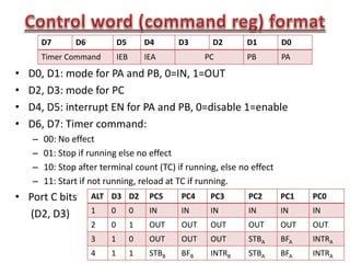
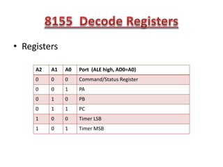
The document discusses the programmable interface device 8155 and its applications. It describes the block diagram and address calculation of the 8155. It then discusses interfacing LEDs and generating square waves using the 8155 timer. It also covers the handshake and interrupt modes of the 8155 and interfacing an A/D converter using the handshake mode. The document provides code examples to initialize ports and display values on ports. It explains using the 8155 to read data from an A/D converter and display it on seven segment LEDs while recording the conversion time.


![Ece iv-fundamentals of hdl [10 ec45]-notes](https://cdn.slidesharecdn.com/ss_thumbnails/ece-iv-fundamentalsofhdl10ec45-notes-150103114952-conversion-gate02-thumbnail.jpg?width=640&height=640&fit=bounds)


