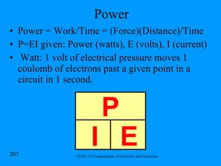
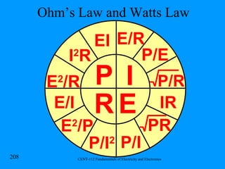
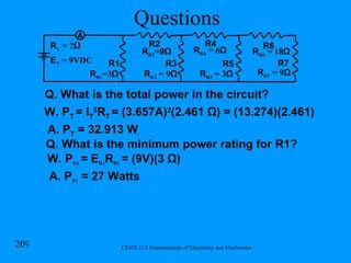
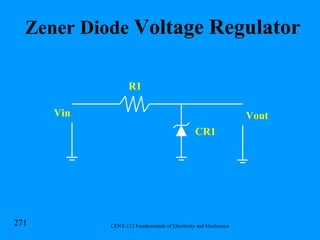
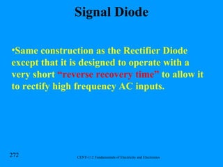
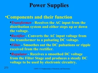
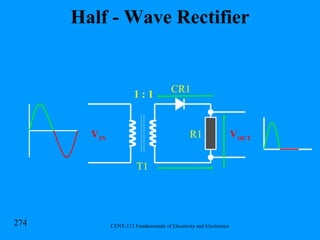
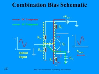
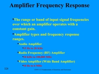
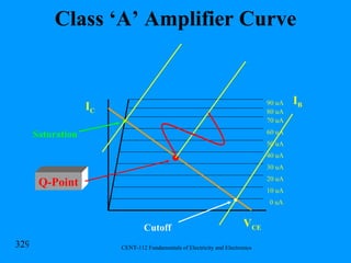
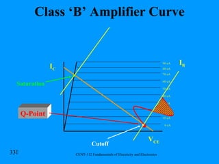
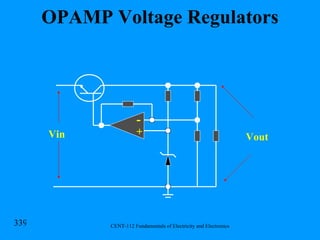
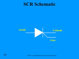
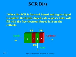
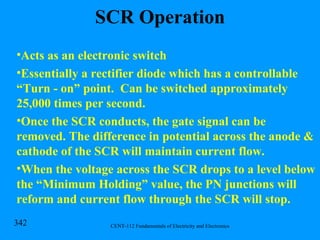
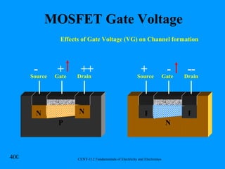
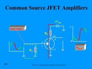
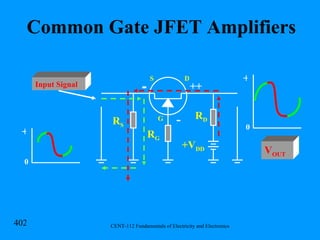
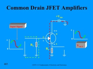
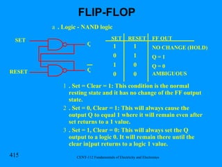
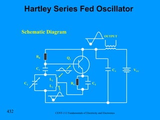
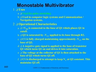
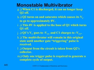
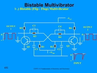
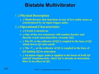
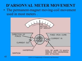
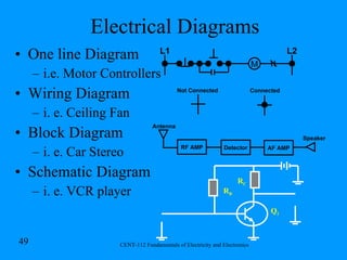
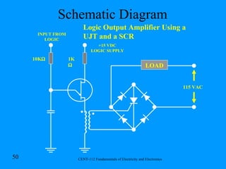
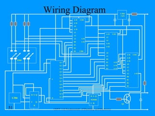
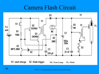
CENT-112: Fundamentals of Electricity & Electronics Dr. Van de Graaff (MIT Professor) designed and built this generator as a research tool in early atom-smashing and high energy X-ray experiments. This is the standard of excellence we should aspire to.
Course Outline Section 1: Fundamentals of Electricity & Electronics Section 2: Basic Circuits Section 3: Motors, Generators, & Power Distribution Section 4: Advanced Electrical Circuits Section 5: Electronic Communication & Data Systems
Interest The great end in life is not knowledge but action. Take your knowledge and use it as soon as you can. “ Use technology as a blessing to mankind and not as a curse.” Einstein 1879-1955 Improvement ideas: tomsic@hawaii.edu Website: http://www.hcc.hawaii.edu/~tomsic 12 labs, 2 projects (audio amplifier & PS) 3 exams
Introduce Yourself Where are you from? How do you like Honolulu Community College? What experience do you have in electronics? What is something interesting about yourself? What do you want to learn in this class?
Section 1: Fundamentals of Electricity & Electronics Safety Precautions Basic Electrical Terms and Circuits Basic Measuring Instruments Basic Electrical Circuit Materials Energy Sources of Electricity
A GOOD THING TO KEEP IN MIND! SAFETY
THE BEST TOOLS EVER INVENTED … HANDS!
SAFETY SHIELDS ARE EYE INSURANCE!
SAFETY SHOES ARE NOT FOR DEFEAT!
HEARING PROTECTION IS FOR WINNERS!
Always check Electrical Circuits Deenergized Discharge capacitors. Check Power Leads (T1-T3) Check Capacitors discharged. < 30VAC is deenergized.
Electrostatic Discharge (ESD) Invisible Threat 1 touch can ruin this card. Wear a wrist strap.
General Safety Rules Do not work when you are tired or taking medicine that makes you drowsy. Do not work in poor light. Do not work in damp areas or with wet or damp clothing and shoes. Use approved tools, equipment, & protective devices. Remove all metal items when working around exposed circuits.
General Safety Rules Continued Never assume that a circuit is off. Double-check it with an instrument that you are sure is operational. Buddy system is used at circuit breaker supplying power if working on circuit. Never override safety interlocks. Keep all tools and test equipment in good working condition. Discharge capacitors.
General Safety Rules Continued Do not remove grounds and do not use adapters that defeat the equipment ground. Use CO 2   or halogenated-type fire extinguisher to put out electrical fires. Water conducts electricity! (i.e. galley fire in oven). Store solvents and other chemicals in appropriate areas. (i.e. fire personnel incident). Do not work on unfamiliar circuits. Do not cut corners or rush. No horseplay or practical jokes in the labs (i.e. throwing caps, meggering).
Shock Victim Do not become part of the problem. Use non-conductive belt and break free shock victim. Call for medical assistance. (911)
Review CPR Check for response. Have someone call 911. Clear airway. Look, listen and feel for breathing. Give 2 full breaths. 15 compressions (1 and 2 and 3) Continue till medical help arrives, you are relieved or are too tired to continue.
Questions Q1. Who is responsible for safety? A1. Everybody is responsible for their safety. Q2. What protects electronic circuits from ESD? A2. ESD packaging & wrist straps. Q3. What is the worst electrical shock  you have heard of or experienced? A3. Various.
Scientific Notation 10 ־ 12 .000000000001 p pico 10 ־ 9 .000000001 n nano 10 ־ 6 .000001 μ micro 10 ־ 3 .001 m milli 1 basic unit 10 3 1,000 k kilo 10 6 1,000,000 M mega 10 9 1,000,000,000 G giga 10 12 1,000,000,000,000 T tera Power of Ten Decimal Symbol Prefix
Ohms Law E I R E=IR Given: E = Voltage I = Current R = Resistance I = E/R R = E/I
Basic Electrical Terms Definitions Current (I): Flow of electrons past a point. 1A = 1 coulomb of charge flowing past a point for 1 second. Unit of measure is amps. Resistance (R): Opposition to the flow of electrons. Unit of measure is ohms. Voltage: (E): Force behind electrical flow. Unit of measure is the volt.
Questions Q4. Given a 1 Megohm resistor with a 120 volt potential applied to it, what current will pass through it? A4. .12 milliamps Q5. Can this current kill you if you touch it? A5. No. .1 Amp for 1 second can be fatal. Q6. How many students know CPR? A6. It is a good thing to be qualified in CPR when working on or near electrical circuits.
Questions Continued Q7. Given a 1.5 Amp battery charger with a total circuit resistance of 8 ohms, what supply voltage is generated? A7. 12 volts Q8. What amperage is present when you place the new chip in your cellular phone? A8. micro amps. Q9. What amperage is present when you put leads on a new car battery? A9. milliamps
Definitions Atomic Theory Foundation for Solid State Devices Atom  - Smallest part of an element that retains the characteristics of that element. Molecule  – Smallest part of a compound. Compound  - 2 or more elements chemically combined.
The Atom Atom Parts: Electrons: Negative part of an atom. Protons: Positive part of an atom. Neutrons: Negative part of an atom. N P N P E E E E E E E E E E
Static Electricity Like charges repel each other and unlike charges attract each other. Walking across a wool or nylon rug , you can generate a static charge of electricity, discharging several thousand volts of electricity to a metallic object like a door handle.
Definitions Coulomb: Practical unit of measurement of the amount of electricity. Used to describe the flow of electricity. 1 Coulomb = 6.24 X 10 18  electrons. Electrostatic or Dielectric field: The field or force surrounding a charged body. Charge Transfer Direct Contact Induction: Electron flow due to charged object in close proximity.
Energy Band Diagrams Valence Electrons  are those electrons which are located in the outermost or  “Valence”  shell of an atom. The number of valence electrons an atoms has determines the electrical properties of that atom. < 4 electrons  =>  Conductor > 4 electrons  =>  Insulator 4 electrons  =>  Semiconductor
Energy Band Diagrams Continued Conductor Semiconductor Insulator Valence Band Forbidden Band Conduction Band
Bonding Covalent  vs.  Ionic   Bonding “ Octet”  Rule and Covalent Bonding “ N”  and  “P”  Crystals Base Material  -  Silicon  or  Germanium Doping  - Process by which impurity atoms are added into a pure base material to create a compound with improved electrical properties. This process is used when making semiconductors.
Static Device Application Electrostatic Precipitator: Collector Plates need cleaning. Oil Mist Mechanical Filter Ionizer Plate: Positively charges Particles in air Collector Plate: Negative plates collects + ions. Clean Air
Basic Electrical Circuit Power Supply (Source) Conductor Load (Light)
Types of Current AC: Alternating Current DC: Direct Current 0 + - 0 + -
Circuit Flow Conventional Current Flow: Hole flow. Electron Flow Series Circuit Parallel Circuit Series/parallel Circuit
Basic Instruments & Measurements Simpson 260 Fluke 177
Interest One of the first meter instruments was used by the Greeks (0 BC) and was the Sun Dial.
Outline Types of meter movement Types of meters Voltmeter Ammeter Ohmmeter Electrical diagrams
Basic Multimeters A meter is a measuring instrument. Ammeter:  measures current. Voltmeter:  measures the potential difference (voltage) between two points. O hmmeter  measures resistance. Multimeter:  combines these functions and others into a single instrument.
Ammeter Measures current in amperes, milliamperes, microamperes depending on the meter scale. The coil in the meter movement is wound with many turns of fine wire. If a large current was allowed to flow the coil, it would burn it out, so a shunt or alternate path is provided for current. Most of the current flows through the shunt. Safety: Connect an ammeter is series with a circuit device.  Never in parallel!
Determining Shunt Resistors Meter movement requires 1mA for full scale deflection. The resistance of the coil is 100 Ω. The ranges of the meter are: 0-1mA, 0-10mA, 0-50mA, 0-100mA. E=IR = (.001)(100) = .1V without a shunt. For full scale deflection, .1V is required. A shunt must carry 90% of the current for the 0-10mA scale. Rs =E/I = .1/.009 = 11.1Ω Calculate the other shunt resistors.
Voltmeter To ensure voltages across the coil never exceed .1V,  multiplier resistors  are placed in series with the meter movement coil using a switch. Voltage ranges 0-1V, 0-10V, 0-100V, 0-500V .1V can be placed across meter at any one time, therefore a resistor must drop .9V to use a 0-1V scale. Full scale current deflection is 1mA or .001A Rm = E/I  + .9V/.001A = 900 Ω Calculate multiplier resistors for other scales.
Ohmmeter Uses non-linier scale: zero-infinite. Calibrate prior to use for analog meter. Check leads at 0 Ω for good lead connections. Electrical leads safety story for finger stop.
Moving Iron Vane Meter
Moving Iron Vane Meter   Measure either AC or DC. It depends on induced magnetism for its operation. It utilizes the principle of repulsion between two concentric iron vanes, one fixed and one movable, placed inside a solenoid. A pointer is attached to the movable vane. When current flows through the coil, the two iron vanes become magnetized with north poles at their upper ends and south poles at their lower ends for one direction of current through the coil. Because like poles repel, the unbalanced component of force, tangent to the movable element, causes it to turn against the force exerted by the springs.
D'ARSONVAL METER MOVEMENT   The permanent-magnet moving-coil movement used in most meters .
D'ARSONVAL METER MOVEMENT   D'Arsonval meter movement is capable of indicating current in only one direction. Without a rectifier, or direct current of the wrong polarity, the meter would be severely damaged. Since the pointer will vibrate (oscillate) around the average value indication, damping is used. Airtight chamber containing a vane  The movement of the coil (conductor) through a magnetic field causes a current to be induced in the coil opposite to the current that caused the movement of the coil.
Digital Multimeters (DMM) DMM are smaller and more accurate in measurement. Analog meters can measure transients information better. Measures resistance, DC & AC voltage, amperage, and diode testing.
Questions Q. What is the difference between diode testing and resistance checking? A. The diode check is more sensitive with an audible sound for continuity. Q. What are some experiences that you have with different meters? A. Various
Electrical Diagrams One line Diagram i.e. Motor Controllers Wiring Diagram i. e. Ceiling Fan Block Diagram i. e. Car Stereo Schematic Diagram i. e. VCR player L1 L2 M RF AMP Detector AF AMP Antenna Speaker Not Connected Connected R C R B Q 1
Logic Output Amplifier Using a UJT and a SCR LOAD INPUT FROM LOGIC 115 VAC 1K  10K  +15 VDC LOGIC SUPPLY Schematic Diagram
Q 1 Q 2 Q 3 Q 4 Q 5 Q 6 Q 7 Q 8 Q 9 Q 10 Q 11 Q 12 C R U306 D  S  Q C  Q R D  S  Q M305B C  R A>B  U300 A=B A0 A<B A1 A2 A3  A=B B0  A<B B1 B2 B3  U300 A>B  U301 A2 A3 A=B A<B A0 A1 B0 B1  A>B B2  A=B B3  A<B A>B  U302 A=B A<B A0 A1 A2 A3  A=B B0 B1 B2 B3 S300 U304 +12V Q1 Wiring Diagram
Conclusion
Basic Electrical Circuit Materials
Interest Optical fiber is a long, cylindrical, transparent material that confines and transmits light waves.  Carries information in the form of light giving the fiber thousands of times more information-carrying capacity than copper, which uses electricity to transmit signals.  3 LAYERS:  1. Core: carries the light (silica glass)  2. Cladding: confines the light to the core (silica glass)  3. Coating: provides protection for the cladding (plastic) Carries information so fast that you could transmit 3 television show episodes in just one second. This is impossible with copper wire.
Basics Conductor: Pathways that allow electrons to flow through an electrical circuit. Electron flow Hole flow (+ charge flow, opposing viewpoint). Materials: Copper: Most common. Silver: Better conductor, more expensive Aluminum: Used in high voltage lines because of its light weight. Center core is steel for strength. Brass: Used in electro-mechanical parts like relays and contactors.
Conductor Sizes American Wire Gauge System The larger the gauge number, the smaller the cross-sectional area the wire will have. Circular Mils (cmil) cmil = Diameter 2 4 cmil = (2 mil wire diameter)  2 1 inch by ¼ inch wire = (1000 mils)(250 mils)/.7854 = 318,309 cmils 0 30 36 15
Conductor Insulation Insulation: Conductor protective coating. Materials: Rubber, plastic and other synthetic materials Factors: Extreme heat, cold, chemicals, and oil. Codings: R: Rubber H: Heat C: Corrosion resistant Types: High voltage, Coaxial, multiple conductors, stranded conductors, solid conductors, 3 conductor lighting cord.
Conductor Resistance Factors that effect resistance. Cross-sectional area of the conductor:  Larger diameter, lower resistance. Type of conductor resistance:  Aluminum 1000 feet = 2.57 ohms. Copper 1000 feet = 1.619 ohms. Length of conductor:  Longer conductor, higher resistance. Temperature of material:  Higher temperature, higher resistance.
Safety Standards National Electrical Code (NEC) is a collection of electrical standards that must be followed to ensure safety of personnel and prevent electrical fires. Maximum voltage drop for branch circuits (i.e. breaker panel to outlet) is 3%. CMA = (K)(I)(L)/VD where CMA = area in cmil, K = constant (K=12 for copper and 18 for aluminum), I = current, L = length of conductor, VD = voltage drop.
Questions Q. Given a copper conductor  for a 20A drill 75 feet away, what size wire is needed? W. Length = (75)(2)=150  VD = (120)(.03)=3.6 CMA = (K)(I)(L)/VD CMA = (12)(20)(150)/3.6 = 10,000 cmils or No. 10 wire.  A. No. 10 wire
Breadboards Copper strips are run in parallel under the rows of holes and are used as conductor pathways. Jumper wires are used to connect all the solid state devices. Used to prototype a circuit.
Breadboards
Printed Circuit Board (PCB)
Printed Circuit Board (PCB) Edge Connectors Heat Sink Connection Pad Conductor Path
Printed Circuit Board (PCB)
Chassis Chassis: Circuit using metal frame providing conduction path for the negative side (ground) i.e. Tail light being supplied by car battery. i. e. Power supply using chassis resisters.
Switches Classified by the actuator which is the mechanical device that causes the circuit to open and close. SPST: Single Pole Single Throw  Single Pole: 1 path for electron flow to be turned on & off. Single Throw: Switch controls only one circuit. DPDT: Double Pole Double Throw Double Pole: 2 paths for electron flow to be turned on & off. Double Throw: Switch controls two circuits.
Toggle Switch
Slide Switch
Rocker Switch
Rotary Switch
Rotary Switch Application
Wafer Switch
Limit Switch
Dip Switch
Questions Q. What is something that uses a limit switch? A. Computer, Camera, Shredder, etc. Q. What is something that uses a dip switch? A. Back of computer to switch 120 to 240 VAC Q. What is something that uses a rocker switch? A. Light switch
Switch ratings Current: Maximum amperage rating to handle current safely. High current causes high heat. Voltage: Maximum voltage rating so that electromechanical circuitry will not fail.
Connectors Splice lug: Connects 2 wires. Wire nut connector: Connect motor with controller.
Wire Cutter Tools
Circuit Protective Devices Fuses: Open/ blow for circuit protection. Circuit Breakers: Protect larger rated equipment. -Positions: on, off, trip-free -Explain troubleshooting ACBs. 120V5A
Incandescent Lamp In 1879 Thomas Edison developed the 1 st  incandescent lamp. The tungsten replaced the carbon filament. The heat produced from current flow is usually what burns out the filament with time. Tungsten
Fluorescent Lamp When the tube is energized, the filaments at the end will glow producing heat and little light. The heat vaporizes the mercury in the tube. Once the mercury is vaporized, electrons flow in the mercury vapor. Ultraviolet light is produced. The light strikes the phosphor coating and causes it to glow creating phosphorous light. (very little heat)
Lighting Physical Diagram Starter Ballast Light Clip
Fluorescent Lighting Schematic
Neon Light 2 Electrodes inserted in the ends of a long glass tube. Tube is filled with neon gas. A neon light transformer ( ≥ 10,000V) is used to create current through the neon gas. After the light is energized, the neon tube will glow. To create a variety of colors, other gasses are added. (i.e. argon and helium)
LED Light
Halogen Lamp A tungsten filament is inserted through a glass tube filled with halogen gas. Produces more light. The halogen gas returns boiled of tungsten particles back to the filament making the filament last longer. Creates high heat. Filaments can be damaged from oil on fingers. light filament
Fiber Lighting from the Sun Future of lighting
Camera Flash Circuit NE: Neon Lamp FL: Flash
Resistors Demonstrate resistor software.
Chip Resistors
Potentiometers Rotary knob varies resistance. Can use an eraser to clean carbon deposits between arm and resistor. Uses: voltage and speed adjust.
Variable Resisters
Wire Wound Resistors Starting Resistors
Conclusion Q. When do a use a resistor in a circuit? A. provide opposition to current flow or develop a voltage drop. Q. What can cause a potentiometer to no longer work? A. Loose or broken arm.
Sources of Electricity
Interest Solar power device use is on the increase. Devices include cars to radios.
Basic Sources of Electricity Friction Chemical Action Light Heat Pressure Magnetism
Battery History Luigi Galvani (1790): Frog supported on copper wires leg twitched when touched with a steel scalpel. Alessandro Volta: Invented electric/ voltaic cell by placing 2 dissimilar elements in a chemical building an electric potential creating electricity from chemical action.
Battery Experiment A grapefruit can be used to produce enough electricity to operate a small radio. Penny Nickel
Zinc Carbon Battery Cell Zn + H 2 SO 4  + H 2 O  ZnSO 4  + H 2 O + H 2 plate + electrolyte + water  sulfated - plate + water + hydrogen gas. End of Life due to H 2  blanketing around carbon rod. H2SO4 + H2O Zn C H 2 - +
Primary Cells AAA Cell AA Cell C Cell D Cell
Primary Cells
Primary Cells Can not be recharged. Chemical action can not be reversed. Defect: Polarization: H 2  blanketing around electrode. Depolarization agent is added to prevent the H 2  blanketing around electrode . Compounds rich in oxygen (i.e. MnO 2 ) are used. The O 2  in the depolarization agent combines with H 2  to form H 2 O. (2MnO 2  + H 2  2MnO 3  + H 2 O):  Local Action: Does not contribute to electrical energy.
Battery Dry Cell Flashlight Batteries: Zinc-carbon Cell
AA Alkaline Cell Anode: Manganese Dioxide Cathode: Zinc Powder Electrolyte: Caustic Alkali Separator: Separates + & -
Mercury Cell New type of dry cell. 1.34 VDC from chemical action between zinc (-) and mercury oxide (+). Costly to make Creates 5 times more current then other dry cells. Maintains terminal voltage longer. Uses: field instruments & portable communications.
Lithium Cell Lithium is bonded to a thin layer of conductive metal and has a porous separator between it and the cathode. This design allows for a large surface area, providing a large reaction surface & higher discharge rates compared to other Lithium cells.
Silver Oxide Cell Uses amalgamated zinc anode, silver oxide as the cathode material, & a potassium hydroxide electrolyte. Silver oxide cells are ideal for miniature devices where space is limited. Voltage: 1.5 to 1.2 V Uses: Watches
Silver Oxide Cell
Secondary Cells Can be recharged or restored. Chemical action can be reversed.
Battery Chargers Used to restore the charge on rechargeable batteries. Used for: AA batteries and car batteries.
Battery Chargers Schematic
Battery Chargers P/S Schematic Parts of a Power Supply Stepdown Transformer Bridge Rectifier Filters Regulator
Battery Charges Normal: Done when battery is discharged Equalizing: Done to drive sulphates off of positive plate. Float: Keep at full charge. Freshening: New batteries
Incidents Battery fire due to charging battery.
Battery Wet Cell
Measuring Specific Gravity Determines state of the charge on the battery.
Lead Acid Battery
Lead Acid Battery Primary Chemical Reactions Pb + PbO 2  + 2H 2  SO 4 -2  2PbSO 4 -2  + 2H 2 O + 5 e - Half Cell Chemical Reactions Pb + SO 4 -2  = PbSO 4 -2  + 2 e - PbO 2  + 4 H +  + 2 e -  + SO 4 -2  = PbSO 4 -2 Pb PbO 2 - + H 2  SO 4 -2 H 2  O Electrolyte Separator charge discharge
Lead Acid Battery Description In a wet cell, the metals are sponge lead (Pb) and lead peroxide (PbO2), and the electrolyte is dilute sulfuric acid (H2SO4).  The reaction begins as sulfate (SO4) breaks away from the acid and unites with the lead of both the positive and negative plates to form lead sulfate (PbSO4).  The oxygen (O2) is thereby liberated from the lead peroxide and joins with the hydrogen (H2 -- what's left over after the sulfate left the acid) to produce ordinary water (H2O), which dilutes the electrolyte.
Lead Acid Battery Plastic Case Terminal Post Terminal Post Separator Plates
Lead Acid Battery Batteries self- discharge 1-25% per month in storage Lead sulfation starts occurring when the state-of-charge drops  below 100%.  If left in a vehicle, disconnecting the negative cable will reduce the level of discharge by eliminating the load.  Cold  will slow the self-discharge process down and  heat  will speed it up. Batteries are recycled by law.
Battery Safety
Nickel-cadmium Cell
Nickel-cadmium Cell Chemical Reaction: 2 NiOOH + 2H 2 O + Cd  2 Ni(OH) 2  + Cd(OH) 2 These batteries contain a Ni(OH)2 cathode, Cd anode and aqueous KOH electrolyte. Ni(OH)2 has a layered CdI2 structure, and NiOOH is apparently a complex, multiphase material.  Advantages: High cycles (often 1000's) and long shelf life (possibly months without significant self-discharge). Disadvantages: Relative to Pb acid include lower power densities, greater cost, and a &quot;memory&quot; effect.  charge discharge Nickel hydroxide Oxy-Nickel hydroxide Cadmium hydroxide
Nickel-cadmium Cell Memory effect: Unused capacity of a cell cannot be utilized if the cell is not fully discharged. Related to the formation of a passive surface on the electrodes that forms a barrier to further cell reaction.
Nickel-cadmium Cell Applications: Cassette players and recorders Dictating machines Instruments  Personal Pagers Photoflash equipment  Portable communications equipment Portable hand tools and appliances  Shavers Tape recorders Toothbrushes
Questions Q. What do you use batteries for? A. Radios, lights, fans, cars, toys, calculators, cameras, laptops. Q. What is the largest battery you have seen? A. Submarine battery. Q. What is the difference between rechargeable and disposable batteries? A. Rechargeable batteries are made of NiCAD while disposable batteries are alkaline because NiCAD can be cycled more.
Dirty Cells cause grounds
Cell Damage
Questions Q. What is the chemical reaction for a lead-acid battery? A.  Pb+PbO 2 +2H 2  SO 4 -2  2PbSO 4 -2 +2H 2 O+5 e - . Q. What is a button battery made of? A. Silver Oxide. Q. If your battery is grounded, how do you repair it? A. clean it & retest or take it to Sears to check the internal resistance. charge discharge
Batteries in Series _ + Physical Description Electrical Schematic + + + + _ _ _ _ Output 6 VDC 1A [email_address] [email_address] [email_address] [email_address]
Batteries in Parallel _ + Physical Description Electrical Schematic _ _ _ + + + + _ Output 1.5 VDC 4A 1.5V @1A 1.5V @1A 1.5V @1A 1.5V @1A
Batteries in Series-Parallel Physical Description Electrical Schematic Output 6 VDC 2A _ + _ _ _ + + + 1.5V @1A 1.5V @1A 1.5V @1A 1.5V @1A + _ 1.5V @1A 1.5V @1A 1.5V @1A 1.5V @1A _ + _ _ _ + + +
Battery Capacity Look at manufacture chart for specifications. Capacity in Amp-Hours (AH) is the ability to produce current over a period of time. Rate of discharge must be considered in order to get maximum AH out of battery. Factors effecting capacity of battery: Number of plates per cell. Kind of separators effect capacity & battery life. General condition of the battery. (i.e. age, grounds, state of charge).
Other Sources of Electricity Solar Heat Crystals Fuel Cells Diesels Generators
Photovoltaic Cell
Photovoltaic Cell Schematic symbol + _ Physical description L _ + P type semiconductor N type semiconductor Sunlight Specifications: 1 cell produces 1 Watt and .5 Volts Cells can be connected into arrays. Arrays are build with cells in series and parallel.
Photovoltaic Cell Application Used to keep solar powered cars charged when not being driven.
Questions Q. What are some applications that you have used a solar cell for? A. Cars, calculators, heat new houses. Q. What is the current and voltage of 6-6 volt, 2 amp batteries placed in parallel in a spotlight? A. 6 Volts and 12 Amps.
Photoresistive Cells Schematic symbol
Photoresistive Cell Application PILOT DEVICE AC OR DC +V CC +V OUT Resistance is proportional to the light source applied. The circuit below uses a photoresistive call to bias the base of a transistor. The output of this amplifier could be used to power a light (Street Light).
Thermocouple Schematic symbol + _ Physical Description Copper Wire Iron Wire Match Galvanometer: Measures very  Small currents. Thermocouple Thermocouple + Galvanometer = Pyrometer Group of thermocouples = Thermopile
Piezoelectric Effect Definition: The property of some crystals (i.e. Quartz) that when a pressure is exerted on one axis, a proportional voltage is present on the other axis. Physical Description: Sound waves Quartz Crystal pressure electrical waves e- Output
Fuel Cells Schematic symbol FC Physical description L Electrolyte Potassium Hydroxide KOH _ + Electrode Electrode Hydrogen Gas Oxygen Gas Operation H 2  gas supplied develops a  –  potential on electrode & ionizes the electrolyte. O 2  gas supplied develops a  +  potential on electrode & ionizes the electrolyte. H 2 O is waste product of chemical reaction with no heat loss. Used in the space program. Ratings: 1.23V, 2KW
Magnetohydrodynamic Generator Magnetohydrodynamic (MHD) electricity is generated when ionized gas is passed through a magnetic field. MHD converter Coil for Magnetic Field + _ Output + _ Anode Plate Cathode Plate Ionizing Gas (Argon or Helium) Ionizing Gas Gas heated by solar power > 2000F
Generator Schematic symbols G Output waveform 0 Phase A Phase B Phase C
Generator Generates 450 VAC, 60 Hz, 3 phase electricity.
Conclusion Q. Explain a way to produce electricity? A. Various Q. What is the output waveform of the Hawaiian Electric Company? A. 3 Phase Sine Wave.
Series Circuits
Interest Knowing how to do calculations in series circuits is one of the basic building blocks in electronics. Electronics software products let you download software to run on your computer testing your knowledge of circuit calculations. Demonstrate in class. Resistor calculator software.
Series Circuit Formulas E T  = E 1  + E 2  + E 3  … + E N R T  = R 1  + R 2  + R 3  … + R N I T  = I 1  = I 2  = I 3  … = I N
Voltage in a Series Circuit E T  = E 1  + E 2  + E 3  … + E N Kirchhoff’s voltage law:  The source voltage of a series circuit is equal to the total value of each individual voltage drop. Example: E T  = 19V E R3  = 4V E R2  = 8v E R1  = 7V R1 R2 R3
Current in a Series Circuit I T  = I 1  = I 2  = I 3  … = I N Total amperes into the circuit is the same across each component that current travels through in a series circuit. Example: I T  = 2mA I R3  = 2mA I R2  = 2mA I R1  = 2mA R3 R2 R1
Resistance in a Series Circuit R T  = R 1  + R 2  + R 3  … + R N Total resistance is equal to the sum of the individual resistances in a series circuit. Total resistance is additive. Example: R3 R2 R1 R 1  = 12 Ω R 2  = 7 Ω R 3  = 6 Ω R T  = 25 Ω
Determining Unknown Voltage E R1  = 5V R1 R2 R3 R4 R5 E T  = 24VDC E R2  = 7V E R4  = 2V E R5  = 1V E R3  = ?V Q. What is the voltage drop across R3? W. 24-(5+7+1+2)= A. 9 VDC
Determining Power E R1  = 2V R1 R2 R3 R4 R5 I T  = 3A E R2  = 3V E R4  = 5V E R5  = 6V E R3  = 4V Q. What is the total power in the circuit? W. (2V)(3A) + (3V)(3A) + (4V)(3A) + (5V)(3A) + (6V)(3A) = 6W  +  9W  +  12W  +  15W  +  18W  = A. 60 Watts Given: Power = EI
Questions E R1  = 1V R1 R2 R3 R4 R5 I T  = 5A E R2  = 2V E R4  = 9V E R5  = 2V E R3  = 3V Q. What is the total power in the circuit? W. (1V)(5A) + (2V)(5A) + (3V)(5A) + (9V)(5A) + (2V)(5A) = 5W  +  10W  +  15W  +  45W  +  10W  = A. 85 Watts
Questions Continued E R1  = 1V R1 R2 R3 R4 R5 E T  = ?VDC E R2  = 3V E R4  = 2V E R5  = 1V E R3  = 5V Q. What is the voltage of the power supply? W. 1+3+5+2+1= A. 12 VDC
Questions Continued E R1  = ?V R1 R2 R3 R4 R5 E T  = 2, 555VDC E R2  = 1KV E R4  = .001MV E R5  = 500V E R3  = 45V Q. What is the voltage of R1? W. 2,555-(1000+45+1000+500)= A. 10 VDC
Using Ohms Law in Series Circuits R1 R2 R3 R4 R5 E R2  = 12V Q. What is the total current in the circuit? W. 12/4= A. 3A R 2  = 4 Ω Given: E = IR
Troubleshooting a Lighting Circuit R1 L1 T1 Isolation Transformer Half Wave Rectifier D1 D2 24VAC I L1 =4A Q. RI has an open (is damaged), what will be the rating Of the new resistor? W. 24/4= A. 6 Ω
Using a Voltmeter R1 R2 R3 R4 F1 SW1 6VDC Open Voltmeter 1 = 6 VDC Voltmeter 2 = 0 VDC + + + _ _ _ 10 Ω 10 Ω 10 Ω 10 Ω
Using a Voltmeter Continued R1 R2 R3 R4 F1 SW1 6VDC Shut Voltmeter 1 = 0 VDC Voltmeter 2 = 1.5 VDC + + + _ _ _ 10 Ω 10 Ω 10 Ω 10 Ω
R1 Shorted R1 R2 R3 R4 F1 SW1 6VDC Shut Voltmeter 1 = 0 VDC Voltmeter 2 = 2 VDC + + + _ _ _ 10 Ω 10 Ω 10 Ω 10 Ω
R1 Open R1 R2 R3 R4 F1 SW1 6VDC Shut Voltmeter 1 = 6 VDC Voltmeter 2 = 0 VDC + + + _ _ _ 10 Ω 10 Ω 10 Ω 10 Ω
Questions R1 R2 R3 R4 F1 SW1 6VDC Shut Voltmeter 1 Voltmeter 2 + + + _ _ _ 10 Ω 10 Ω 10 Ω 10 Ω Q. Fuse 1 has blown, what will be the voltage across it? A. 6 VDC Q. Fuse 1 has blown, what will be the voltage across R1? A. 0 VDC
Conclusion Q. How is E, I, R calculated in series circuits? A.  1. E T  = E 1  + E 2  + E 3  … + E N  2. R T  = R 1  + R 2  + R 3  … + R N 3. I T  = I 1  = I 2  = I 3  … = I N Q. What voltage is read across a shorted resister in a series circuit? A. 0 V
Parallel Circuits
Interest The resistors in chips 2X scale 10X scale
Parallel Circuit Formulas I T  = I 1  + I 2  + I 3  … + I N E T  = E 1  = E 2  = E 3  … = E N R T  = 1/(1/R 1  + 1/R 2  + 1/R 3  … + 1/R N ) R T  =R 1 R 2 /(R 1  + R 2 )
Parallel Circuit Voltage E R1  = 24V R1 R2 R3 R4 E T  = 24VDC E R2  = ?V E R4  = 24V Q. What is the voltage drop across R2? W.  E T  = E R2 A. 24 V E R3  = 24V E T  = E 1  = E 2  = E 3  … = E N
Kirchhoff’s Current Law The algebraic sum of all currents entering any point will equal the sum of all currents leaving that point. Simply stated: The current flowing into a junction of parallel resistance is equal to the current flowing out of the same junction. Branch current: Individual currents. Mainline current: Total current.
Parallel Circuit Current I R1  = 5A R1 R2 R3 R4 I T  = 16A I R2  = ?A I R4  = 1A Q. What is the current passing through R2? W. I R2  = I T  – (I R1  + I R3  + I R4 ) = 16 – (5 + 8 + 1) A. 2A I R3  = 8A I T  = I 1  + I 2  + I 3  … + I N I T  = 16A
Parallel Circuit Resistance R R1  = 34 Ω R1 R2 R3 R4 R T  = ? Ω R R2  =  17Ω R R4  =  4.25Ω Q. What is the total resistance in the circuit? W. R RT   = 1/(1/R R1  + 1/R R2  + 1/R R3  + 1/R R4  )   = 1/(1/34 + 1/17 + 1/8.5 + 1/4.25) = 1/(1/34 + 2/34 + 4/34 + 8/34) = 1/(15/34) = 34/15 A. RT = 2.27Ω R R3  =  8.5Ω R T  = 1/(1/R 1  + 1/R 2  + 1/R 3  … + 1/R N )
Parallel Circuit Resistance R R1  = 34 Ω R1 R2 R T  = ? Ω R R2  =  17Ω Q. What is the total resistance in the circuit? W. R T  = R 1 R 2 /(R 1  + R 2 ) = (34)(17)/(34 +17)  = 578/51 A. RT = 11.33 Ω R T  =R 1 R 2 /(R 1  + R 2 )
Parallel Circuit Resistance R R1  = 7.5K Ω R1 R2 R T  = ? Ω R R2  =  250Ω Q. What is the total resistance in the circuit? W. R T  = R 1 R 2 /(R 1  + R 2 ) = (7500)(250)/(7500 + 250)  = 1,875,000/7750 A. RT = 241.94 Ω R T  =R 1 R 2 /(R 1  + R 2 )
Parallel Circuit Resistance R R1  = 3.4K Ω R1 R2 R3 R4 R T  = ? Ω R R2  =  2.1KΩ R R4  =  2.1KΩ Q. What is the total resistance in the circuit? W. R RT   = 1/(1/R R1  + 1/R R2  + 1/R R3  + 1/R R4  )   = 1/(1/3.4 + 1/2.1 + 1/1.6 + 1/2.1) = 1/(.294 + .476 + .625 + .476) = 1/(1.871) A. RT = .534KΩ R R3  =  1.6KΩ R T  = 1/(1/R 1  + 1/R 2  + 1/R 3  … + 1/R N )
Parallel Circuit Equal Resistance R R1  = 8K Ω R1 R2 R3 R4 R T  = ? Ω R R2  =  8KΩ R R4  =  8KΩ Q. What is the total resistance in the circuit? W. R RT   =  R/N   = 8KΩ/4 A. RT = 2KΩ R R3  =  8KΩ R T  = R/N
Parallel Circuit Troubleshooting R1 R2 R3 R4 E T  = 24VAC Q. What must be checked before working on a circuit? A. No voltage in circuit. Voltmeter = 0 VAC L2 L1 T1 T2 Fuses Removed
Questions Q. What law can be used to do calculations in parallel circuits A. Ohms Law Q. Given a total resistance of 12KΩ, what would be the equal parallel resistance for 4 resistors in parallel? W. R = R RT /N = 12KΩ/4 A. 4KΩ
Parallel Circuit Troubleshooting R1 R2 R3 R4 Q. What caused the fuses to blow? A. R1 shorted. Ohmmeter = 0 Ω L2 L1 T1 T2 Fuses Blown E T  = 24VAC R R2  =  250Ω R R1  =  250Ω R R3  =  250Ω R R4  =  250Ω
Parallel Circuit Troubleshooting R1 R2 R3 R4 E T  = 24VAC Q. What fault is present in this circuit and why? R4 is open.  R t  should be 3 Ω for 4 parallel  equal resistors. R 4  is visually open. L2 L1 T1 T2 Fuses Removed R R1  =  12Ω R R2  =  12Ω R R3  =  12Ω R R4  =  12Ω Ohmmeter = 4 Ω
Parallel Circuit Troubleshooting R1 R2 R3 R4 E T  = 24VAC L2 L1 T1 T2 R R1  =  4Ω R R2  =  2Ω R R3  =  2Ω R R4  =  4Ω Ammeter = ?A A. 667mA? Q. What is total circuit current indicated on the ammeter?
Conclusion Q. How must an ammeter always be connected in a circuit? A. In series Q. What is a fault condition that can cause fuses to blow or circuit breakers to trip open? A. Shorted circuit component.
Series-Parallel (Combination) Circuits
Interest Camera resistors: small and precise.
Reducing a Complex Circuit Total Resistance: Equivalent resistance in a circuit. Series-Parallel Circuit: Combination circuit. Reduce combination circuit to a simple series circuit.
Reducing to a Simple Series Circuit R R1  = 6K Ω R1 R2 R T  = ? Ω R R2  =  400Ω Q. What is the total resistance in the circuit? W. R R1-R2  = R 1 R 2 /(R 1  + R 2 ) = (6)(.4)/(6 + .4)  = 2.4/6.4 R R1-R2  = .375 KΩ R R1-R2-R3  = R R1-R2  + R 3   = .375 + 1.6 A. R T  = 1.975K Ω R3 R R3  = 1.6K Ω Step 1
Reducing to a Simple Series Circuit Q. What is the total resistance in the circuit? W.  R R1-R2  = R 1  + R 2  = 4 + 20 = 24 Ω R R1-R2-R3  = R R1-R2 R 3 /(R R1-R2  + R 3 ) = (24)(12)/(24 + 12)  = 288/36 = 8 Ω R R1-R2-R3-R4  = R R1-R2-R3  + R 4  = 8 + 12 A. R T  = 20 Ω R R1 =4 Ω R1 R2 R T  = ? Ω R R2 = 20Ω R3 R R3  = 12 Ω Step 1 R R4  = 12 Ω R4 Step 2
Reducing to a Simple Series Circuit Q. What is the total resistance in the circuit? W.  R R1-R2  = R 1  + R 2  = 3 + 6 = 9 Ω R R1-R2-R3  = R R1-R2 R 3 /(R R1-R2  + R 3 ) = (9)(9)/(9 + 9)  = 81/18 = 4.5 Ω R R5-R6  = R 5  + R 6  = 18 + 9 = 27 Ω R R4-R5-R6  = R R5-R6 R 4 /(R R5-R6  + R 4 ) = (27)(12)/(27 + 12)  = 324/39 = 8.308 Ω R R1-6  = R R1-R2-R3  + R R4-R5-R6  = 4.5 Ω + 8.308 Ω A. R T  = 12.808 Ω R R1 =3 Ω R1 R2 R T  = ? Ω R R2 = 6Ω R3 R R3  = 9 Ω Step 1 R R4  = 12 Ω R4 Step 2 R5 R6 R R5  = 18 Ω R R6  = 9 Ω Step 3 Step 4 E T  = 10VDC
Using Ohms Law Formulas for the last circuit: Determine overall values. E T /R T =I T Determine individual values using series & parallel rules. E R1-R2-R3 =I T R R1-R2-R3 E R1-R2-R3 =E R3 E R3 /R R3 =I R3 I T -I R3 =I R1-R2 I R1 =I R2 =I R1-R2 E R1 =I R1 R R1 E R2 =I R2 R R2
Ohms Law Combination Circuit 1 Q. What is the total current in the circuit? W. I T =E T /R T =10/ 12.808 R R1 =3 Ω R1 R2 R T  = ? Ω R R2 = 6Ω R3 R R3  = 9 Ω Step 1 R R4  = 12 Ω R4 Step 2 R5 R6 R R5  = 18 Ω R R6  = 9 Ω Step 3 Step 4 E T  = 10VDC A. I T =.7808A Q. What is the current passing through R 4 ? W. E R4-R5-R6 =I T R R4-R5-R6 =(. 7808)(8.308)=6.487V E R4-R5-R6 =E R4 =6.487V I R4 =E R4 /R R4 =6.487/12 A. I R4 =.5406A
Ohms Law Combination Circuit 2 R R1 =3 Ω R1 R2 R T  = ? Ω R R2 = 6Ω R3 R R3  = 9 Ω Step 1 R R4  = 12 Ω R4 Step 2 R5 R6 R R5  = 18 Ω R R6  = 9 Ω Step 3 Step 4 E T  = 10VDC Q. What is the current passing through R 5 ? W. I R5 =I T -I R4 =   (.7808)-(.5406) A. I R5  =.2402A Q. What is the current passing through R 6 ? W. I R6 =I R5 A. I R6 =   . 2402A
Ohms Law Combination Circuit 3 R R1 =3 Ω R1 R2 R T  = ? Ω R R2 = 6Ω R3 R R3  = 9 Ω Step 1 R R4  = 12 Ω R4 Step 2 R5 R6 R R5  = 18 Ω R R6  = 9 Ω Step 3 Step 4 E T  = 10VDC Q. What is the voltage passing through R 5 ? W. E R5 =I R5 R R5 =   (.2402)(18) A. E R5  =4.3236V Q. What is the voltage passing through R 6 ? W. E R6 =I R6 R R6 =   (.2402)(9) or E R6 =E R5-R6 -E R5 =6.487- 4.324  A. E R6  =2.1618V
Ohms Law Combination Circuit 4 Q. What is the ammeter reading in the circuit? W. I T =E T /R T =10/12.808 R R1 =3 Ω R1 R2 R T  = ? Ω R R2 = 6Ω R3 R R3  = 9 Ω Step 1 R R4  = 12 Ω R4 Step 2 R5 R6 R R5  = 18 Ω R R6  = 9 Ω Step 3 Step 4 E T  = 10VDC Q. What is the current passing through R 3 ? W. E R1-R2-R3 =I T R R1-R2-R3 =(.7808)(4.5)=3.5136V E R1-R2-R3 =E R3 =3.5136V or E t -E R4-R5-R6 = 10-6.487=3.513V I R3 =E R3 /R R3 =3.5136/9 A. I R3 =.3904A A A. I T =.7808A
Ohms Law Combination Circuit 5 R R1 =3 Ω R1 R2 R T  = ? Ω R R2 = 6Ω R3 R R3  = 9 Ω Step 1 R R4  = 12 Ω R4 Step 2 R5 R6 R R5  = 18 Ω R R6  = 9 Ω Step 3 Step 4 E T  = 10VDC Q. What is the current passing through R 1 ? A. I R1 =.3904A A W. I R1 =I T -I R3 =   (.7808) - (.3904) Q. What is the current passing through R 2 ? W. I R1 =I R2 A.  I R2 =   .3904A
Ohms Law Combination Circuit 6 R R1 =3 Ω R1 R2 R T  = ? Ω R R2 = 6Ω R3 R R3  = 9 Ω Step 1 R R4  = 12 Ω R4 Step 2 R5 R6 R R5  = 18 Ω R R6  = 9 Ω Step 3 Step 4 E T  = 10VDC A Q. What is the voltage passing through R 1 ? W. E R1 =I R1 R R1 =   (.3904)(3) A. E R1  =1.1712V Q. What is the voltage passing through R 2 ? W. E R2 =I R2 R R2 =   (.3904)(6) or E R2 =E R1-R2 -E R2 =3.513-1.171  A. E R2  =2.342V
Sample Problem 1 Q. What is the total resistance in the circuit? W.  R R4-R5  = R 4  + R 5  = 4 + 8 = 12Ω R R3-R4-R5  = R R4-R5 R 3 /(R R4-R5 +R 3 )=(12)(6)/(12+6)  = 72/18 = 4Ω R R2-R3-R4-R5  = R R3-R4-R5 +R R2 =4+2=6Ω R R1-5 =R R2-R3-R4-R5 R R1 /(R R2-R3-R4-R5 +R R1 )=(6)(6)/(6+6)  = 36/12 A. R T = 3Ω R R1 =6 Ω R1 R2 R T  = ? Ω R R2 = 2Ω R3 R R3  = 6 Ω R R4  = 4 Ω R4 R5 R R5  = 8 Ω E T  = 12VDC A
Sample Problem 1 Continued 1 Q. What does the ammeter read in the circuit? W. I T =E T /R T =12/3 A. I T =4A Q. What is the current passing through R 1 ? W. E T =E R1 =12V I R1 =E R1 /R R1 =12/6 A. I R1 =2A R R1 =6 Ω R1 R2 R T  = ? Ω R R2 = 2Ω R3 R R3  = 6 Ω R R4  = 4 Ω R4 R5 R R5  = 8 Ω E T  = 12VDC A
Sample Problem 1 Continued II Q. What is the current passing through R 2 ? W. E T =E R2-R3 =12V I R2 =I R2-R3 =E R2-R3 /R R2+(R3,R4,R5) =12/(2+4) A. I R2 =2A Q. What is the voltage drop across R 2 ? W. E R2 =I R2 R R2=  (2)(2) A. E R2 =4V Q. What is the voltage drop across R 3 ? W. E R3 =E T - E R2  = 12-4 A. E R3 =8V R R1 =6 Ω R1 R2 R T  = ? Ω R R2 = 2Ω R3 R R3  = 6 Ω R R4  = 4 Ω R4 R5 R R5  = 8 Ω E T  = 12VDC A
Sample Problem 1 Continued III Q. What is the current passing through R 4 ? W. E R3 =E R4-R5 =8V I R3 =E R3 /R R3 =8/6=1.3A I R4 =I R2 - I R3 =2 - (1.333) Kirchhoffs Current Law A. I R4 =.6667A Q. What is the voltage drop across R 4 ? W. E R4 =I R4 R R4=  (. 6667)(4) A. E R4 =2.667V Q. What is the voltage drop across R 5 ? W. E R5 =I R5 R R5=  (. 6667)(8) A. E R5 =5.333V R R1 =6 Ω R1 R2 R T  = ? Ω R R2 = 2Ω R3 R R3  = 6 Ω R R4  = 4 Ω R4 R5 R R5  = 8 Ω E T  = 12VDC A
Sample Problem 1 Continued IV Q. Explain Kirchhoffs Current Law. W. I T =I point1  + I point2  + I point3 =2 + (1.333) + (.666) = 4A A. Total current in circuit = current out of circuit. Q. Why isn’t the voltage drop across R 3  = 12VDC? W. E R2 =I R2 R R2=  (2)(2) = 4VDC 4 VDC is subtracted because of the nature of voltage in a series circuit within a combination circuit. Point 1 Point 2 Point 3 R R1 =6 Ω R1 R2 R T  = ? Ω R R2 = 2Ω R3 R R3  = 6 Ω R R4  = 4 Ω R4 R5 R R5  = 8 Ω E T  = 12VDC A
Questions R R1 =3 Ω R1 R2 R T  = ? Ω R R2 = 9Ω R3 R R3  = 9 Ω R R4  = 6 Ω R4 R5 R R5  = 3 Ω E T  = 9VDC A Q. What is the current passing through R 2 ? A. I R2 =.6667A R6 R R6  = 18 Ω R7 R R7  = 9 Ω W. R R6-R7 =R R6  +   R R7 =18+9=27 Ω R R5-R6-R7  =R R6-R7 R 5 /(R R6-R7 +R 5 )=(27)(3)/(27+3)=81/30= 2.7Ω R R4-7 =R R5-7  +   R R4 =2.7+6=8.7 Ω R R3-7  = R R4-7 R 3 /(R R4-7 +R 3 )=(8.7)(9)/(8.7+9)=78.3/16.7=4.689Ω R R2-7 =R R3-7  +   R R2 = 4.689 +9=13.689 Ω R T  = R R2-7 R R1 /(R R2-7 +R R1 )=(13.689)(3)/(13.689+3)= 41.066/16.689 =2.461Ω I T =E T /R T =9/2.461= 3.657A I R1 =E R1 /R R1 =9/3=3A  I R2 =I T - I R1 = 3.657- 3
Power Power = Work/Time = (Force)(Distance)/Time P=EI given: Power (watts), E (volts), I (current) Watt: 1 volt of electrical pressure moves 1 coulomb of electrons past a given point in a circuit in 1 second. P I E
Ohm’s Law and Watts Law P I E R EI I 2 R IR PR P/R P/E E/R E 2 /R E 2 /P E/I P/I 2 P/I
Questions R R1 =3 Ω R1 R2 R T  = ? Ω R R2 = 9Ω R3 R R3  = 9 Ω R R4  = 6 Ω R4 R5 R R5  = 3 Ω E T  = 9VDC A Q. What is the total power in the circuit? A. P T  = 32.913 W R6 R R6  = 18 Ω R7 R R7  = 9 Ω W. P T  = I T 2 R T  = (3.657A) 2 (2.461  Ω) = (13.274)(2.461) Q. What is the minimum power rating for R1? W. P R1   = E R1 R R1   = (9V)(3  Ω) A. P R1  =  27 Watts
Troubleshooting Eliminate parallel paths when checking electrical components.
Conclusion R R1 =2.4K Ω R1 R2 R R2 = 3.6KΩ R3 R R3  = 1.2K Ω E T  = 120VAC A Q. What is the total power in the circuit in KW? A. P T  = 192KW W. W. R R2+R3 = R R2  +  R R3   = (3600 Ω )+(1200  Ω)= 4800Ω R T =R R2+R3 R R1 / R R2+R3 + R R1  =( 4800)(2400)/4800+2400= 11520000/7200=1600Ω  P T   = E T R T   = (120V)(1600  Ω) G
Series Tuned Circuits . Theory . Ideal Series resonant circuit contains no resistance. It contains only inductance and capacitance that are in series with each other and with the source voltage. . Operation . At Resonance ( X L  = X C  ); therefore, X L  + X C  = 0. The resultant reactance is equal to 0. Impedance ( Z ) is minimum.  . Since Z is minimum, current is maximum for a given voltage. Maximum current flow causes maximum voltage drops across individual reactances. Tuned Circuits
Questions Q. What is the formula for XL?  A. XL = 2 II f L. Q. What is the formula for XC? A. XC = 1 / 2 II f C. Q. What is the resonant frequency in a typical tuned circuit? A. XL = XC, Fr = .159/Square root LC.
. Operation (Continued) . When Frequency is < Resonance: X C     => current is lower => voltage drops across reactances are lower. . When Frequency is > Resonance: X L     => current is lower => voltage drops across reactances are lower. Tuned Circuit Operation
. Series Tuned Circuit (Schematic) C1 L1 R1 GEN Tuned Circuit Operation
. Series Tuned Circuit Analysis X L X C o R = Z 0 o X C  - X L X C X L o BELOW RESONANCE CURRENT IMPEDANCE RESONANCE Z = R ABOVE RESONANCE X L X L  - X C X C o 100 200 300 500 600 700 F r Capacitive Inductive Resistive Tuned Circuit Operation
1.  Theory . Called a “tank” circuit because it can store energy. . It has the ability to take the energy fed to it from a power source and store this energy alternately in the inductor and capacitor. . The resulting output is a continuous ac sine wave.  . Operation .  Voltage is the same across the inductor and capacitor. (parallel) . Current through the components varies inversely with their reactances. . Total current through the circuit is the vectoral sum of the two individual component currents. . I L  and I C   are 180 o  out of phase. . At resonance, I L  and I C  cancel each other out => no current from source.  Parallel Tuned Circuits
. Application  .  At resonance, the circuit has a maximum impedance which results in minimum current drawn from the source .
4. Schematic Circuit C1 L1 R1 GEN Parallel Tuned Circuits
. Circuit analysis I C  - I L I C I L o BELOW RESONANCE CURRENT IMPEDANCE RESONANCE ABOVE RESONANCE I L I L  - I C I C o 100 200 300 500 600 700 F r I L I C o I Z Capacitive Inductive Resistive Parallel Tuned Circuits
. Applications . Tuned Amplifier L 1 R L + 0 V IN +V CC R B C 1 C C 0 I MAX T Parallel Tuned Circuits
Questions Q. What are some examples of a parallel tuned amplifiers? A. Antenna tuners, air signal tracker, ham radio, transponders (ID aircraft etc). Q. What crystal can replace the RLC circuit to make it last longer? A. Piezoelectric Crystal.
. Pulsed Amplifier: 3 main sections 1. Gain Amp 2. Input Gate Signal 3. Tank Circuit L 1 + 0 V IN +V CC R 1 C 2 C 1 OUTPUT SIGNAL Pulsed Amplifier
INPUT GATE T 0 T 1 T 2 T 3 OUTPUT SIGNAL Pulsed Amplifier
c. Tuned Amplifier: 3 main sections 1. Gain Amp 2. Positive Feedback Circuit 3. Frequency Determining Device L 1 + 0 V IN +V CC R 1 Cy1 C 1 OUTPUT SIGNAL Tuned Amplifier
SATURATION SATURATION CUTOFF CUTOFF OUTPUT INPUT C1 C2 R2 R1 Q1 +V CC -V EE Overdriven Amplifier
. The input signal drives the transistor into and out of saturation and cutoff. . When the transistor is in saturation and / or cutoff, that portion of the input waveform is “clipped” and the output is distorted. Overdriven Amplifier
Magnetism and Relays
Interest The magnetic field of the sun
Experiments Using Magnets Ring magnets Horseshoe magnet Bar magnets Ferris magnets Coils
Phobos Large Magnet
Basic Magnetic Principles Magnetic Poles South Pole North Pole Magnetic lines of force exist between the north and south poles. Like poles repel. Opposite poles attract. Each magnetic line of force is an independent line. None of the lines cross or touch a bordering line. Natural Magnets: Lodestones were used by mariners for navigation. The Earth is a large magnet surrounded by a magnetic field. (i.e. degaussing coils).
Questions Q. What are some uses for magnets? A. Relays, Levetron, hold things in place. Q. How can a magnet loose its magnetism? A. Pounding or dropping magnets upsets the molecular alignment and weakens the magnet. Heat sources also destroy magnets by causing increased molecular activity, expansion and a return to the molecules random positions.
Magnetic Flux Magnetic flux: The many invisible lines of magnetic force surrounding a magnet. B= Φ /A  B=Flux density in gauss (webers per square centimeter) Φ (phi)=Number of lines A=Cross sectional area in square centimeters 3 rd  Law of Magnetism:  The attractive force increases as the distance of the distance between the magnets decrease. Magnetic force varies inversely with (Distance) 2
LHR for Coils Thumb:  Points in direction Of flux Fingers:  Wrap around coil In direction of current
Magnetism in a Coil Q. What is the direction of flux in this coil? W. Use LHR for coils. A. Thumb points right.
LHR for Conductors Thumb:  Points in direction of current. Fingers:  Wrap around coil In direction of circular magnetic Field.
Magnetism Tools Magneprobe
Magnetism Computer Programs Used for component design.
Reluctance Φ =F/R Φ = Total number of lines of magnetic force in gilberts. F= Force producing the field. R= Resistance to the magnetic field. (Reluctance)
Electromagnets Parts of Electromagnets Iron Core Coil Residual Magnetism: Retentivity of the iron core.
Electromagnet Diagram Q. What type of diagram is this? A. Wiring Diagram.
Magnetic Relay
Magnetic Relay Continued Relay: Device used to control a large flow of current by means of a low voltage, low current circuit. A relay is a magnetic switch. Coil: Attracts armature because of magnetism. Armature: Lever Arm. Contacts: Normally open (NO) Normally closed (NC) Relay Maintenance: Burnishing tool cleans contacts Silver plated armatures should be replaced if there is exposed copper.
Magnetic Relay Physical Description
Timing Relay Timing Relays energize contacts for a specific amount of time based on the adjustable setting. Contacts are timed on and off.
Relay Controller Schematic 20A 120 VAC, 60 HZ, 1 Φ Stop Button Start Button Reset Button M 20A A M1 TR2 M2 TR B E E TR1 C B D A A C M2 M1 ~ E D
Magnetic Circuit Breaker Parts Operating Mechanism Tripper Bar Arc Chutes Frame Rack out mechanism Indication
Manual Breakers Manual breakers are shut locally at the switchboard. Magnetic circuit breakers are shut remotely from a control station.
Doorbell
Buzzer Circuit
Magnetic Shields Shielding is done using the permeability of some other substance. Magnetic lines of force flow through the path of least resistance. N S Shield
Magnetic Levitation Transportation
Magnetic Levitation Transportation HSST is a  magnetic levitation  transportation system that has been developed in Japan by HSST Development Corporation established in 1993. The HSST is magnetically-levitated (not supported by wheels) and is propelled by a linear induction motor (LIM), not by conventional rotary electric motors.
Conclusion Q. How does a relay work? A. Coil energizes, armature engages, secondary contact shuts/opens. Q. When would a use a magnetic circuit breaker? A. Used in electric plants to parallel generators and switchboards. Q. What is the LHR for conductors? A. Fingers: wrap around coil. Thumb: points in direction of current.
Diodes Impurity Atoms: Trivalent : Boron (B), Aluminum (Al), Gallium (Ga), Indium (ln). Has three (3) valence electrons. Known as an  “Acceptor Impurity.” Pentavalent : Phosphorous (P), Arsenic (As), Antimony (Sb), and Bismuth (Bi). Has five (5) valence electrons. Known as a  “Donor Impurity.”
PN Material “ N - Type”  Material: Pure base material doped with a Donor Impurity. Majority  Current Carrier:  Electrons Minority  Current Carrier:  Holes “ P - Type”  Material: Pure base material doped with an Acceptor Impurity. Majority  Current Carrier:  Holes Minority  Current Carrier:  Electrons
Construction Old Method:  Grown Crystals . Newer Methods: Alloy Fused:  N & P material made using heat / pressure. Diffused:  N & P gas and heat. Both methods are used to produce a “PN” Junction.
Questions Q) What is meant by a donor impurity? A) 5 valiant electrons in outer shell. Q) What are 4 examples of a donor impurity? A) Phosphorous, Arsenic, Antimony and Bismuth.
Diode Definitions Potential Hill (Junction Barrier) :  Electrostatic field set up across a PN junction which prevents further combination of majority current carriers. The value of the voltage of the potential hill depends on the type of base material used during diode construction.  1. Silicon (.5 - .8V) 2. Germanium (.2V) Rated for up to 1500A / 3000V. Used primarily in Rectifiers.
Operations & Definitions Forward Bias:  External voltage applied  which opposes the potential hill, effectively reducing the width and resistance of the depletion region. => Majority Current Carriers flow through the PN junction.  Reverse Bias:  External voltage applied  which aids the potential hill, effectively increasing the width and resistance of the depletion region. => No Majority Current Carriers flow through the PN junction.
Rectifier Diode Block Diagram +  +  + +  P  + +  +  + Anode Cathode Potential Hill (Junction Barrier) Depletion Region -  -  - -  N  - -  -  - - - - - - - - - + + + + + + + +
Rectifier Diode Schematic Diagram Anode Cathode
Diode Forward Bias +  +  + +  P  + +  +  + Anode Cathode Potential Hill (Junction Barrier) Depletion Region -  -  - -  N  - -  -  - -  -  -  -  +  +  +  +  + -
Diode Reverse Bias +  +  + +  P  + +  +  + Anode Cathode Potential Hill (Junction Barrier) Depletion Region -  -  - -  N  - -  -  - -  -  - -  -  - -  -  - -  -  - + + + + + + + + + + + + + -
Characteristic Curve +I (mA) Forward Bias Reverse Bias -I (uA) Avalanche Breakdown +V a -c -V a -c
Zener Diode The  Zener diode  is a heavily doped diode which, as a result of doping, has a very narrow depletion region. This allows the diode to be operated in the reverse biased region of the characteristic curve without damaging the PN junction. “ Zener Effect”:  The area of Zener diode operation  (<5V)  where the Diode maintains a constant voltage output while operating reverse biased. “ Avalanche Effect”:   >5V  applied to the diode while reverse biased which tends to cause the diode to eventually breakdown due to heat generation within the lattice structure of the crystal.
Zener Diode  Schematic Symbol Anode Cathode
Characteristic Curve Operating Region Reverse Bias Forward Bias + V a - c - V a - c I (mA) I (uA)
Zener Operation Ratings: .25V to 1500V Used in SSMG / SSTG AC voltage regulator for the reference circuit. When a higher constant voltage is desired, the zener diodes will be  “Stacked”  together in series and their voltages will add together to make the higher desired voltage. This is the case in the SSMG / SSTG AC voltage regulators where four (4) 6v zener diodes are stacked to provide a 24V reference to the comparison circuit.
Zener Diode  Voltage Regulator R1 CR1 Vin Vout
Signal Diode Same construction as the Rectifier Diode except that it is designed to operate with a very short  “reverse recovery time”  to allow it to rectify high frequency AC inputs.
Power Supplies Components and their function Transformer  - Receives the AC input from the distribution system and either steps up or down the voltage. Rectifier  - Converts the AC input voltage from the transformer to a pulsating DC voltage. Filter  - Smoothes out the DC pulsations or ripple received from the rectifier. Regulator  - Receives a smoothed DC voltage from the Filter Stage and produces a steady DC voltage to be used by electronic circuitry.
Half - Wave Rectifier V OUT V IN 1 : 1 T1 CR1 R1
Half - Wave Rectifier Operation Positive half-cycle the diode is Forward Bias (FB), negative half-cycle the diode is Reverse Bias (RB).  V DC  = V PK  X .318 Where: V DC   = Average DC voltage    V PK   = Peak input voltage   .318 = Constant
Full - Wave Rectifier V OUT V IN 1 : 1 T1 CR1 R1 CR2
Full - Wave Rectifier Operation Positive half-cycle, 1 diode is FB, negative half-cycle the other diode is FB.  V DC  = V PK  X .637 Where: V DC   = Average DC voltage    V PK   = Peak input voltage   .637 = Constant
Full – Wave Bridge Rectifier V OUT V IN 1 : 1 T1 CR1 R1 CR2 CR3 CR4
Full - Wave Bridge  Rectifier Operation Positive half-cycle, 1 diode is FB, negative half-cycle the other diode is FB.  V DC  = V PK  X .637 Where: V DC   = Average DC voltage    V PK   = Peak input voltage   .637 = Constant
Filters A filter uses the characteristics of Inductors and Capacitors to smooth the pulsating DC waveform supplied by the Rectifier. Types High Pass  - A series RC filter whose output is taken from the resistor. Series / Parallel  - A filter configuration which uses combinations of capacitors and inductors to smooth the voltage and current pulsations from the rectifier output.
Ideal filter characteristics Rapid charge time constant for filter capacitors and inductors. Slow discharge time constant for filter capacitors and inductors.
Capacitor Filter Configuration R B C 1 V IN V OUT Capacitor Input Filter Schematic Diagram
Capacitor Filter Operation Charge RC time constant is developed from the  internal resistance of the rectifier diodes  and the  capacitance of the filter capacitor . The net result is that the low resistance of the rectifier diodes develop a rapid charge RC time constant. Discharge RC time constant is developed from the  filter capacitor  and the  load resistance . Since the load resistance is rather large, the discharge RC time constant is somewhat long. R B  is called the  “Bleeder Resistor”  because it provides a path for the filter capacitor(s) to discharge when power is removed from the circuit. R B  has a very large resistance and usually draws <10% of normal operating current.
LC Choke Filter Configuration LC Choke Filter Schematic Diagram R B C 1 V IN V OUT L 1
LC Choke Filter Operation Charge RC time constant is developed from the  internal resistance of the rectifier diodes, the Low DC resistance of the inductor (L1),  and the  capacitance of the filter capacitor . The net result is that the low resistance of the rectifier diodes and inductor (L1) develop a rapid charge RC time constant. Discharge RC time constant is developed from the  filter capacitor  and the  load resistance . Since the load resistance is rather large, the discharge RC time constant is somewhat long. The Inductor acts to smooth out the current pulsations produced by the rectifier and / or transformer stage of the power supply.
RC PI Filter Configuration RC PI Filter Schematic Diagram R B C 2 V IN V OUT C 1 R 1 V OUT(C1) V OUT (C2) Charge Path Discharge   Path
RC PI Filter Operation First Capacitor  provides most of the filtering action. Second Capacitor  Provides additional voltage filtering. Resistor  limits current flow to the desired value and establishes the RC time constants for both filter capacitors.
LC PI Filter Configuration LC PI Filter Schematic Diagram R B C 2 V IN C 1 L 1 V OUT(C1) V OUT (C2) Charge Path Discharge   Path
LC PI Filter Operation First Capacitor  provides most of the filtering action. Second Capacitor  Provides additional voltage filtering. Inductor  opposes changes in current flow to reduce current spikes and establishes the RC time constants for both filter capacitors.
Voltage Regulators R1 CR1 Vin Vout Series Regulator Acts as a variable resistor in series with the load. Zener Diode Voltage Regulator Schematic
Voltage Regulator Operation R1 CR1 Vin Vout V IN V OUT
Transistor Voltage Regulators Vin Vout
OPAMP Voltage Regulators Vin Vout - +
Tubes, Transistors and Amplifiers
Interest In 1947,   Bardeen & Brattain at Bell Laboratories created the first amplifier!   Shockley (boss), came near to canceling the project. The three shared a Nobel Prize. Bardeen and Brattain continued in research (and Bardeen later won another Nobel). Shockley quit to start a semiconductor company in Palo Alto. It folded, but its staff went on to invent the integrated circuit (the &quot;chip&quot;) & to found the Intel Corporation.
Tetrode Tube Control Grid:  Controls amplification rate & electron flow with bias voltage. Shield:  Screen grid- increases electron speed cathode to + plate. Heater:  Heats gas to gas amplification state. Inert Gas:  Mercury or Argon gas. (+) Plate (-) Shield Control Grid (-) Cathode Heater Inert Gas
Cathode Ray Tube (CRT) (+) Anode (-) Cathode 3 Electron Beams (Red, Green, Blue) Grids Phosphor Coated Screen Conductive Coating The  cathode  is a heated filament (like light bulb filament) in a vacuum inside a glass tube. The ray is a stream of electrons that naturally pour off a heated cathode into the vacuum.  The  + anode  attracts the electrons pouring off the cathode. In a TV's CRT, the stream of electrons is focused by a focusing anode into a tight beam and then accelerated by an accelerating anode. This tight, high-speed beam of electrons flies through the vacuum in the tube and hits the flat screen at the other end of the tube. This screen is coated with phosphor, which glows when struck by the beam.
Bipolar Transistors History Created in 1948 in the AT&T Bell Laboratories. Scientists were performing doping experiments on semiconductor material (diodes) and developed a semiconductor device having three (3) PN junctions.
Bipolar Transistor Construction NPN / PNP Block Diagrams Emitter Emitter N  P  N P  N  P Collector Base Base Collector
Bipolar Transistor Theory For  any  transistor to conduct, two things must occur. The  emitter - base PN junction  must   be forward biased.  The  base - collector PN junction  must   be reverse biased.
Bipolar Transistor Biasing (NPN) + N  P  N Emitter Base + - FB RB Collector
Bipolar Transistor Biasing (PNP) P  N  P Emitter Collector Base + + - FB RB
Bipolar Transistor Operation (PNP) The + emitter repels the majority current carriers towards the emitter - base PN junction. Majority current carriers pass through the forward biased emitter - base junction and flow into the base. Once in the base, these current carriers now become minority current carriers and are attracted to the strong negative voltage applied to the collector. 90% of the current carriers pass through the reverse biased base - collector PN junction and enter the collector of the transistor.  10% of the current carriers exit transistor through the base. The opposite is true for a NPN transistor.
Amplifier Operation The transistor below is biased such that there is a degree of forward bias on the base - emitter PN junction. Any input received will change the magnitude of forward bias & the amount of current flow through the transistor. The magnitude of the output will be on the order of 1000x larger depending on the value of +V CC . R B R C Q 1 + 0 +V CC Input Signal + 0 Output Signal
Amplifier Electric Switch Operation When the input signal is large enough, the transistor can be driven into saturation & cutoff which will make the transistor act as an electronic switch. Saturation  -  The region of transistor operation where a further increase in the input signal causes no further increase in the output signal. Cutoff   - Region of transistor operation where the input signal is reduced to a point where minimum transistor biasing cannot be maintained => the transistor is no longer biased to conduct. (no current flows)
Amplifier Electric Switch Operation Transistor Q-point Quiescent point  : region of transistor operation where the biasing on the transistor causes operation / output with no input signal applied. The biasing on the transistor determines the amount of time an output signal is developed. Transistor Characteristic Curve This curve displays all values of I C  and V CE  for a given circuit.   It is curve is based on the level of DC biasing that is provided to the transistor prior to the application of an input signal. The values of the circuit resistors, and V CC  will determine the location of the Q-point.
Transistor Characteristic Curve I C V CE Q-Point I B 0 uA 10 uA 20 uA 30 uA 40 uA 50 uA 60 uA 70 uA 80 uA 90 uA Saturation Cutoff
Transistor Maintenance When troubleshooting transistors, do the following: Remove the transistor from the circuit, if possible. Use a transistor tester, if available, or use a digital multimeter set for resistance on the  diode scale . Test each PN junction separately. ( A “front to back” ratio of at least 10:1 indicates a good transistor).
Transistor Maintenance Chart This chart shows the readings for a good transistor. Transistor Maintenance
Transistor Maintenance Chart Advantages of junction transistors over point contact transistors: -Generate less noise. -Handles more power. -Provides higher current and voltage gains. -Can be mass produced cheaply.
Questions Q) What is the 7 step troubleshooting method? A) Symptom recognition, symptom elaboration, list possible faulty functions, identify faulty function, identify faulty component, failure analysis, repair, retest. Q) What was the most difficult problem you ever troubleshot? A) Various
Bipolar Transistor Amplifiers Amplifier Classification Amplifiers can be classified in three ways: Type (Construction / Connection) Common Emitter Common Base Common Collector Bias (Amount of time during each half-cycle output is developed). Class A, Class B, Class AB, Class C Operation Amplifier Electronic Switch
Common Emitter Schematic R B R C Q 1 + 0 +V CC Input Signal + 0 Output Signal Output Signal Flow Path Input Signal Flow Path
Kirchoff Voltage Law DC Kirchoff Voltage Law Equations and Paths R B R C Q 1 +V CC Base - Emitter Circuit I C R C  + V CE  - V CC  = 0 I B R B  + V BE  - V CC  = 0 Collector - Emitter Circuit
Common Emitter Operation Positive Going Signal Negative Going Signal Output Signal Input Signal + + 0 0 Base becomes more (+) WRT Emitter   FB      I C       V R C      V C       V OUT     ( Less + ) Base becomes less (+) WRT Emitter   FB      I C       V R C      V C       V OUT     ( More + ) R C R B Q 1
Common Base Schematic + 0 + 0 +V CC R B R C R E Q 1 C C Input Signal Flow Path Output Signal Flow Path
Kirchoff Voltage Law DC Kirchoff Voltage Law Equations and Paths +V CC R B R C R E Q 1 C C Base - Emitter Circuit I B R B  + V BE  + I E R E  - V CC  = 0 Collector - Emitter Circuit I C R C  + V CE  + I E R E  - V CC  = 0
Common Base Operation Positive Going Signal Negative Going Signal +V CC R B R C R E Q 1 C C Base becomes more (+) WRT Emitter   FB      I C       V R C      V C       V OUT     ( More + ) Base becomes less (+) WRT Emitter   FB      I C       V R C      V C       V OUT     ( Less + ) Input Signal 0 Output Signal + 0
Common Collector Schematic R B R E Q 1 + 0 +V CC Input Signal + 0 Output Signal Output Signal Flow Path Input Signal Flow Path
Kirchoff Voltage Law DC Kirchoff Voltage Law Equations and Paths R B R E Q 1 +V CC Base - Emitter Circuit I B R B  + V BE  + I E R E  - V CC  = 0 Collector - Emitter Circuit I C R C  + V CE  + I E R E  - V CC  = 0
Common Collector Operation Positive Going Signal Negative Going Signal R B R E Q 1 +V CC Base becomes more (+) WRT Emitter   FB      I E       V R E      V E       V OUT     ( More + ) Base becomes less (+) WRT Emitter   FB      I E       V R E      V E       V OUT     ( Less + ) Input Signal 0 0 + + Output Signal
AZAZA VOPINI & House of BEC Common  Common  Common B  E  C  Av = Voltage Gain Zo = Output Impedance Ap = Power gain Zin = Input  Impedance Ai = Current Gain
Transistor Bias Stabilization Used to compensate for temperature effects which affects semiconductor operation.  As temperature increases, free electrons gain energy and leave their lattice structures which causes current to increase.
Types of Bias Stabilization Self Bias :  A portion of the output is fed back to the input 180 o  out of phase.  This negative feedback will reduce overall amplifier gain. Fixed Bias :  Uses resistor in parallel with Transistor emitter-base junction. Combination Bias :  This form of bias stabilization uses a combination of the emitter resistor form and a voltage divider. It is designed to compensate for both temperature effects as well as minor fluctuations in supply (bias) voltage. Emitter Resister Bias :  As temperature increases, current flow will increase. This will result in an increased voltage drop across the emitter resistor which opposes the potential on the emitter of the transistor.
Self Bias Schematic R B R C Q 1 +V CC + = Initial Input Self Bias Feedback Resulting Input + + + + o o o o V OUT
Emitter Bias Schematic R B R C Q 1 +V CC + o V OUT R E ++ + + - - Initial Input + o C E DC Component AC Component
Combination Bias Schematic R B1 R C Q 1 +V CC + o V OUT R E ++ + + - - Initial Input + o C E DC Component AC Component R B2
Amplifier Frequency Response The range or band of input signal frequencies over which an amplifier operates with a constant gain. Amplifier types and frequency response ranges. Audio Amplifier 15 Hz to 20 KHz Radio Frequency (RF) Amplifier 10 KHz to 100,000 MHz Video Amplifier (Wide Band Amplifier) 10 Hz to 6 MHz
Class ‘A’ Amplifier Curve I C V CE I B 0 uA 10 uA 20 uA 30 uA 40 uA 50 uA 60 uA 70 uA 80 uA 90 uA Saturation Cutoff Q-Point
Class ‘B’ Amplifier Curve I C V CE I B 0 uA 10 uA 20 uA 30 uA 40 uA 50 uA 60 uA 70 uA 80 uA 90 uA Saturation Cutoff Q-Point
Class ‘AB’ Amplifier Curve I C V CE I B 0 uA 10 uA 20 uA 30 uA 40 uA 50 uA 60 uA 70 uA 80 uA 90 uA Saturation Cutoff Q-Point Can be used for guitar distortion.
Class ‘C’ Amplifier Curve I C V CE I B 0 uA 10 uA 20 uA 30 uA 40 uA 50 uA 60 uA 70 uA 80 uA 90 uA Saturation Cutoff Q-Point
Amplifier Coupling Methods D irect : The output of the first stage is directly connected to the input of the second stage.  Best Frequency Response  - No frequency sensitive components. I mpedance (LC) Coupling : Similar to RC coupling but an inductor is used in place of the resistor.  Not normally used in Audio Amplifiers. R C Coupling :  Most common form of coupling used.  Poor Frequency Response. T ransformer Coupling : Most expensive form coupling used.  Mainly used as the last stage or power output stage of a string of amplifiers.
Direct Coupling Schematic R B1 R C1 Q 1 +V CC 1 R B2 R C2 Q 2 +V CC 2
RC Coupling Schematic R B1 R C1 Q 1 +V CC 1 R B2 R C2 Q 2 C C +V CC 2
Impedance Coupling Schematic R B1 Q 1 +V CC 1 R B2 R C2 Q 2 C C +V CC 2
Transformer Coupling Schematic R B1 R C1 Q 1 +V CC 1 R B2 R C2 Q 2 +V CC 2 T 1
Silicon Controlled Rectifiers Silicon Controlled Rectifiers (SCR) Construction Block Diagram Anode Cathode Gate P P N N Left Floating Region
OPAMP Voltage Regulators Vin Vout - +
SCR Schematic Anode Cathode Gate
SCR Bias Anode Gate P P N N Cathode - FB FB RB + + When the SCR is forward biased and a gate signal is applied, the lightly doped gate region’s holes will fill with the free electrons forced in from the cathode.
SCR Operation Acts as an electronic switch Essentially a rectifier diode which has a controllable “Turn - on” point.  Can be switched approximately 25,000 times per second. Once the SCR conducts, the gate signal can be removed. The difference in potential across the anode & cathode of the SCR will maintain current flow. When the voltage across the SCR drops to a level below the “Minimum Holding” value, the PN junctions will reform and current flow through the SCR will stop.
SCR Phase Control The term Phase Control refers to a process where varying the timing of the gate signal to an SCR will vary the length of time that the SCR conducts. This will determine the amount of Voltage or Power delivered to a load.
Unijunction Transistors (UJT) Construction:  Originally called “Double-based Diodes.” “ P” Type material doped into the “N” type base material. Placement of the Emitter into the Base determines the voltage level (%) at which the the UJT fires. This % is called the  “Intrinsic Standoff Ratio (     ).” Once constructed, the Intrinsic Standoff Ratio cannot be changed. The actual voltage value at which the UJT fires is determined by the amount of source voltage applied.
UJT Block Diagram Emitter Base 2 Base 1 P N Emitter Base 2 Base 1 Equivalent Circuit
UJT Schematic Symbol Emitter Base 2 Base 1
UJT No Operation When V E  is less than or equal to the voltage base one to emitter requirement (V E - B1 ), the UJT will not fire.  Emitter Base 1 Base 2 P N ++ - + No Current Flow Depletion Region
UJT Operation Emitter Base 1 Base 2 P N ++ - + UJT Fires V E  > V E-B1 When V E  is more than the voltage base one to emitter requirement (V E - B1 ), the UJT will fire.
UJT Sawtooth Generator R 1 C 1 Q 1 E B 1 B 2 V BB SW 1 V OUT C 1  Discharge C 1  Charge
UJT Relaxation Oscillator R 1 C 1 Q 1 V BB SW 1 V OUT 1 C 1  Discharge C 1  Charge RB 2 RB 1 V OUT 2 V OUT 3 V OUT 2 V OUT 3 + + + V OUT 1
UJT Relaxation Oscillator The output of the Oscillator can be used for sweep generators, gating circuit for SCR’s, as well as timing pulses for counting and timing circuits.
Lessons Learned Video Card ruined from ESD < 20 V (Improper Handling). Bad Inductor in a regulator detected with Huntron Tracker.  Slightly different oval.
Summary Q) What is the phase relationship between input and output voltage in a common emitter circuit? A) 180 degrees.
Summary Continued Q) What type of transistor bias uses both self and fixed bias? A)  Combination bias. Q) What is the frequency response range of an RF amplifier? A) 10Khz – 100, 000 Mhz.
. Silicon Bilateral Switch (SBS) . Construction A2 A1 G P P N J1 J2 A2 A1 G
. Schematic Symbol Anode 2 Anode 1 A2 A1 Gate
. Characteristic Curve V  A2-A1 I (mA) Holding Current (I HO ) Reverse Breakover Voltage Forward Breakover Voltage Breakback Voltage
. Characteristics . More vigorous switching characteristic.   V to almost zero. . More temperature stable. . More symmetrical wave form output. . Popular in low voltage trigger control circuits. . Theory . Lower breakover voltages than Diac. (+/- 8V is most popular). . SBS has more pronounced “Negative Resistance” region. . It’s decline in voltages is more drastic after it enters the conductive state.
. Operation . As shown below, if a zener diode is placed in the gate circuit between “G” and “A1”, the forward breakover voltage (+V BO ) can be altered to approximately that of the zener voltage (V Z ). . -V BO  is unaffected. SBS A2 A1 G
. Characteristic Curve V  A2-A1 I (mA) Holding Current (I HO ) Reverse Breakover Voltage Forward Breakover Voltage Breakback Voltage
Silicon Unilateral Switch (SUS) Construction P P N N Anode Cathode Gate
. Schematic Symbol Anode Cathode Gate
Theory Similar to the four (4) layer diode except the +V BO  can be altered by using the gate terminal voltage. Operation V  A-C -V  A-C I Forward Breakover Voltage Reverse Breakdown Voltage { } Much greater than Forward Breakover Voltage
. Varactor . Construction P N
. Theory . For testing purposes, a front to back ratio of 10:1 is considered normal. . The size of the depletion region in a varactor diode is directly proportional to the amount of bias applied. . As forward bias increases, capacitance (Depletion region) decreases. . As reverse bias increases, capacitance (Depletion region) increases. . In the capacitance equation below, it is shown that only the distance between plates can be changed. C =  Ak d Where: A = Plate Area k = Constant d = Distance between plates
. An increase in reverse bias increases the width of the gap (d) which reduces the capacitance of the PN junction and vice versa. . Advantage: Allows DC voltage to be used to tune a circuit for simple remote control or automatic tuning function. . Operation . used to replace old style variable capacitor tuning circuits. .  They are used in tuning circuits of more sophisticated communications equipment and in other circuits where variable capacitance is required.
3V 6V 20  F 5  F P N P N Depletion Region
.  Special Purpose Amplifiers . Differential Amplifier .  Schematic Diagram + V CC - V EE R E R B  (1) R C  (1) R C  (2) R B  (2) Q 1 Q 2 V OUT V IN  (1) V IN  (2)
.  Operation + V CC - V EE R E R B  (1) R C  (1) R C  (2) R B  (2) Q 1 Q 2 V OUT V IN  (1) V IN  (2) + - (+)  / (-) ARE ASSIGNED BY WHICH VOLTMETER LEAD IS USED AS THE REFERENCE + 0 + 0 ++ ++ + + - - + 0 V OUT
.  With the polarities shown previously: . On positive going signal, Base of Q1 becomes more (+) with respect to emitter => FB Q 1     => I C Q1     => V RC1     => V C Q1      (less +).  Since I C Q1    => I E Q1     (I E     = I C     + I B ) => V RE     => Emitter of Q2 becomes less (-) with respect to Base =>  FB Q2     => I C Q2     => V RC2    =>  V C Q2     (more +). Due to the polarities assigned by our voltmeter, the difference between Q1 and Q2 is becoming less => V OUT      (Negative Going). .  On negative going signal, Base of Q1 becomes less (+) with respect to emitter => FB Q 1     => I C Q1     => V RC1     => V C Q1     (more +).  Since I C Q1    => I E Q1     (I E     = I C     + I B ) => V RE     => Emitter of Q2 becomes more (-) with respect to Base =>  FB Q2     => I C Q2     => V RC2    =>  V C Q2     (less +). Due to the polarities assigned by our voltmeter, the difference between Q1 and Q2 is becoming larger => V OUT      (Positive Going).
.  With the resulting output achieved, it can be said that a positive going input on the base of Q1 caused VCQ1 to be inverted => the base of Q1 is called the “Inverting Terminal.” Since the positive going input caused VCQ2 to increase in a positive direction, the base of Q2 is called the “Non-Inverting Terminal.” . If my voltmeter leads were changed, the output of the amplifier would also change. The Inverting and Non-Inverting terminals would also change.
.  Operational Amplifiers (OPAMPS) .Block Diagram (Basic) DIFFERENTIAL AMPLIFIER VOLTAGE AMPLIFIER OUTPPUT AMPLIFIER NON-INVERTING INPUT INVERTING INPUT + - + v CC - v EE OUTPUT
.  Ideal OPAMP Characteristics .  Infinite (  ) Input Impedance Draws little or no current from source. .  Zero Output Impedance .  Infinite (  ) Gain .  Infinite (  ) Frequency Response Constant gain over any range of input signal frequencies.
.  Types of OPAMPS .  Linear (Output is Proportional to Input) .  Inverting + - V OUT V IN R F R 1 + 0 + 0 + -
.  Non - Inverting + - V OUT V IN R F R 1 + 0 + 0 + -
.  Summing + - V OUT V IN 1 R F R 5 + 0 + 0 + - V IN 4 + 0 V IN 3 + 0 V IN 2 + 0 V IN 1 V IN 2 V IN 3 V IN 4 R 1 R 2 R 3 R 4
.  Difference + - V OUT V IN 1 R F + 0 + 0 + - V IN 4 + 0 V IN 3 + 0 V IN 2 + 0 V IN 1 V IN 2 V IN 3 V IN 4 R 1 R 2 R 3 R 4 V IN 5 0 + R 5 V IN 5
.   Non - Linear (Output is not Proportional to Input) . Comparator + - V OUT V IN + 0 + 0 + - - V REF V REF  ATTACHED TO EITHER  + OR - TERMINALS  (EXAMPLE SHOWS OUTPUT WITH V REF  CONNECTED TO THE NON-INVERTING TERMINAL.) (WAVEFORM WOULD BE INVERTED IF V REF  WAS ATTACHED TO THE INVERTING TERMINAL) V IN V REF V OUT
.  Differentiator + - V OUT V IN R F R 1 + 0 + 0 + - C 1
.  Integrator + - V OUT V IN R 1 + 0 + 0 + - C 1
Field Effect Transistors (FETs) Field Effect Transistor Types Junction Field Effect Transistors (JFETs) (N and P Channel) JFETs are voltage sensitive devices that use voltage vice current to control output. Current does not flow through a PN junction; however, a PN junction is used to control the size of a channel and to control current flow.
N Channel JFET Source Drain Gate N P P Channel P P P P N Depletion Region -- - ++
P Channel JFET Drain Gate P N N Channel N N N N P Depletion Region -- ++ +
JFET Schematic Symbols Gate Gate Drain Source Source Drain N - Channel P - Channel
JFET Characteristic Curve Ohmic Region Pinchoff Region Avalanche Region V SD I D 0
JFET Operation Regions Ohmic Region : As V SD  increases, Drain Current (I D ) increases in a nearly linear manner. Pinchoff Region : As V SD  increases, Drain Current (I D ) remains constant. Avalanche Region : As V SD  increases, Drain Current (I D ) increases uncontrollably and control of the FET is lost.
JFET Operation  The voltage applied to the gate of a FET is reverse bias in nature and determines the size of the channel. When gate voltage (V G ) is large enough, the depletion regions touch and drain current (I D ) is cut off (Channel is Pinched Off).  This is called the “Pinchoff Voltage.” With Gate Voltage (VG) held constant, as VSD increases, Drain Current (ID) increases and vice versa.  This assumes that the FET is operating in the ohmic region of the characteristic curve.
JFET Operation  V G  = 0 V G  = 1 V G  = 2 V SD I D 0
MOSFETs Metal Oxide Semiconductor Field Effect Transistors (MOSFETs) MOSFETs where originally called “IGFETs” due to the insulated gate portion of the the FET’s construction.  MOSFETs are extremely susceptible to damage from electrostatic discharge.
Depletion Mode MOSFET P Source Gate Drain Metal Oxide Layer P Source Gate Drain N N -  -  ++ +  +  --
Depletion Mode MOSFET Schematic Symbols Drain Gate Source Drain Gate N - Channel P - Channel
Depletion Mode MOSFET Curve I D V G 0
N Channel MOSFET Operation N Channel Depletion MOSFET Biasing / Operation Negative (-) on the Source, Positive (+) on the Drain, and Negative (-) on the gate. Negative (-) on the gate will induce positive ions in channel which creates an area within the channel where there are no majority current carriers. (Depletion Region) The amount of Gate voltage (V G ) applied will determine the size of the channel thereby controlling the amount of current flow through the transistor.
P Channel MOSFET Operation P Channel Depletion MOSFET Biasing / Operation Positive (+) on the Source, Negative (-) on the Drain, and Positive (+) on the gate. Positive (+) on the gate will induce negative ions in channel which creates an area within the channel where there are no majority current carriers. (Depletion Region) The amount of Gate voltage (V G ) applied will determine the size of the channel thereby controlling the amount of current flow through the transistor. N & P Channel Depletion MOSFET Biasing / Operation Depending on the polarity of the gate voltage (VG) applied, the depletion mode MOSFET can be made to operate either in the depletion mode or enhancement mode.
Enhancement Mode MOSFET Block Diagrams (N & P Channel) P Source Gate Drain Metal Oxide Layer Source Gate Drain N N N P P -  +  ++ +  -  --
Enhancement Mode MOSFET Schematic Symbols (N & P Channel) Drain Gate Source Gate N - Channel P - Channel
Enhancement Mode MOSFET Curve I D V G 0
N Channel MOSFET Operation N Channel Enhancement MOSFET Biasing / Operation The Depletion region Creates / “Enhances” channel formation. The amount of Gate voltage (V G ) applied will determine the size of the channel thereby controlling the amount of current flow through the transistor.
P Channel MOSFET Operation P Channel Enhancement MOSFET Biasing / Operation The Depletion region Creates / “Enhances” channel formation. The amount of Gate voltage (V G ) applied will determine the size of the channel thereby controlling the amount of current flow through the transistor.
MOSFET Gate Voltage Effects of Gate Voltage (VG) on Channel formation P Source Gate Drain Source Gate Drain N N N P P -  +  ++ +  -  --
Common Source JFET Amplifiers R G R D +V DD G S D ++ + 0 Input Signal V OUT - -
Common Gate JFET Amplifiers R G R D +V DD G S D ++ + 0 + 0 Input Signal V OUT - - R S
Common Drain JFET Amplifiers + 0 + 0 Input Signal V OUT R G R S +V DD G S D ++ - -
Lessons Learned MOSFET ruined from ESD < 20 V static electricity. Computer laptop not working anymore when soda spilled on keyboard. Computer motherboard overheated when cooling fan seized due to accumulation of dust over the years. New computer BIOS chip ruined upon installation because not using the proper tool.
Logic Circuits . Boolean Algebra . Developed by George Boolean, a 19th century mathematician. . His theories were used to develop an assembly  of gears and pulleys to be used to drive a grain elevator.  . A Boolean expression is nothing more than a description of the input conditions necessary to get a desired output.
. Theorem . A rule concerning a simple relationship between variables. . Postulate . A basic statement that is accepted as valid. . Only two statements are true. . X = 0 and X = 1 Theorems and Postulates
1. . Distributive Law.  (Repeating) . Example: A + (B * C) = (A + B) * (A + C)  or A*(B+C) = A*(B+C) = (A*B) + (A*C) . Double Negative Law. . A = A . DeMorgan’s Law A + B = A * B  or  A*B = A + B Law of Intersection A(1) = A A(0) = 0 Law of Union A + 1 = 1 A + 0  = A Laws and Theorems
Logic Symbols (Gates) . Logical functions can be expressed in one of four (4) ways.) . English Statement . Boolean Expression . Truth Table . Logic Symbol . “AND” Gate . The “AND” function is considered to be logical multiplication.  . Any multiplication symbol can be used to express the “AND” function. (X, *, ( )( ), etc) Logic Gates
. English Statement - A and B equals Z . Boolean Expression - A X B = Z, AB = Z, (A)(B) = Z, A*B = Z etc. . Truth table . Logic Symbol A B Z 0 0 0 0 1 1 1 1 1 0 0 0 Z B A AND Gate
. The “OR” function is considered to be logical addition. . English Statement - A or B equals Z . Boolean Expression - A + B = Z . Truth table . Logic Symbol A B Z 0 0 0 0 1 1 1 1 1 1 1 0 Z B A OR Gate
. Inverter “NOT” gate  . The “NOT” function is considered to be logical inversion. . English Statement - NOT “A” equals Z . Boolean Expression - A = Z . Truth table . Logic Symbol A Z 0 0 1 1 Z A NOT Gate
. “NOR” gate  . English Statement - NOT A or B equals Z . Boolean Expression - A + B = Z . Truth table . Logic Symbol A B Z 0 0 0 0 1 1 1 1 0 0 0 1 Z B A NOR Gate
. “NAND” gate  . English Statement - NOT A and B equals Z . Boolean Expression - A X B = Z, AB = Z, (A)(B) = Z, A*B = Z etc. . Truth table . Logic Symbol A B Z 0 0 0 0 1 1 1 1 0 1 1 1 Z B A NAND Gate
. “XOR” gate  . English Statement - A exclusively or’d to B equals Z . Boolean Expression - A + B = Z . Truth table . Logic Symbol A B Z 0 0 0 0 1 1 1 1 0 1 1 0 Z B A XOR Gate
. Logic - NAND logic . Set = Clear = 1: This condition is the normal resting state and it has no change of the FF output state. . Set = 0, Clear = 1: This will always cause the output Q to equal 1 where it will remain even after set returns to a 1 value. . Set = 1, Clear = 0: This will always set the Q output to a logic 0. It will remain there until the clear in[put returns to a logic 1 value. SET RESET Q Q SET RESET FF OUT 1 0 1 1 1 0 0 0 NO CHANGE (HOLD) Q = 1 Q = 0 AMBIGUOUS FLIP-FLOP
. SET = CLEAR = 1: This condition tries to “Set” and “Clear” the FF continuously and can produce an ambiguous result. Do not use. . Logic- “NOR” logic SET RESET Q Q SET RESET FF OUT 1 0 1 1 1 0 0 0 NO CHANGE (HOLD) Q = 0 Q = 1 AMBIGUOUS FLIP-FLOP
. Set - Clear Flip Flop . High Input Responding (Logic High) SET CLEAR FF OUT 1 0 1 1 1 0 0 0 NO CHANGE (HOLD) Q = 1 Q = 0 AMBIGUOUS SET CLEAR FF Q Q FLIP-FLOP
. Low Input Responding (Logic low) SET CLEAR FF Q Q SET CLEAR FF OUT 1 0 1 1 1 0 0 0 NO CHANGE (HOLD) Q = 1 Q = 0 AMBIGUOUS FLIP-FLOP
. JK Flip - Flop . Logic Symbol J K FF Q Q CLK PS CLR FLIP-FLOP
. Truth Table PRESET  CLEAR  CLOCK  J  K  Q  Q 0  0  X  X  X  1  1 0  1  X  X  X  1  0 1  0  X  X  X  0  1 1  1     0  0  Q  Q 1  1     1  0  1  0 1  1     0  1  0  1 1  1     1  1  TOG GLE 1  1  0  X  X  Q  Q INPUTS  OUTPUTS FLIP-FLOP
Bipolar Integrated Circuit Logic
Resistor - Transistor Logic (RTL)
Diode - Transistor Logic (DTL)
High - Threshold Logic (HTL)
Transistor - Transistor Logic (TTL)
Direct - Coupled Transistor Logic (DCTL)
Emitter - Coupled Transistor Logic (ECTL)
Integrated Injection Logic (IIL)
Oscillating Circuits
. Tickler  (Armstrong)  Oscillator . Schematic Diagram V CC R C R E R B C B C E C 1 Q 1 T 1 OUTPUT FEEDBACK L 1 NPN 1  3 2  4 Transistor Oscillators
b.  Physical Description .) Uses an LC tuned circuit to establish the base frequency. .) Feedback accomplished by mutual inductance coupling between the tickler coil and the LC tuned circuit. .) Uses class “C” amplifier with self - bias.  .  Operational characteristics .) Output frequency relatively stable. .) Output amplitude is relatively constant. .) RF frequency range .) Local Oscillator in receivers. .) Source in signal generators. .) Radio - frequency oscillators in the medium and high frequency range. Tickler (Armstrong) Oscillator
Schematic Diagram V CC C 3 C E C 1 C 2 R B R E L 2 L 1 Q 1 OUTPUT Hartley Series Fed Oscillator
.) Physical Description .) Can generate a wide range of frequencies and is easy to tune. .)  Current Flows through the tank circuit in the series-fed, but not used in the shunt fed. .) Operational Characteristics .) Ordinary Operation: Class “C” amplifier with self-bias. .) When output waveform must be constant voltage of a linear wave shape => Class “A” amplifier is used. Hartley Series Fed Oscillator
.) Operation (Voltage applied to circuit) .) Current flows from battery (V CC ) through L3 from collector to emitter, through R E , through L1, and back to the battery. .) The surge of current through coil L1 induces a voltage in L2 to start tank circuit oscillations. .) When current first starts to flow through coil L1, the bottom of L1 is negative with respect to the top of L2.  .) The voltage induced into coil L2 makes the top of L2 positive. .) As the top of L2 becomes positive, the positive potential is coupled to the base of Q1 via C1. .) An increasing (+) on the base of Q1 causes forward bias to increase => I C  increases => I E  increases => I L1  increases and results in more energy being supplied to the tank circuit which in turn increases the (+) at the top of L2 and increases the forward bias on Q1. Hartley Series Fed Oscillator
.) This action continues to raise and lower the potential on the base of Q1 to control the output current. .) L1 feeds the tank circuit with energy that is lost during normal operation. (REGENERATIVE FEEDBACK). .) L2’s magnetic field expands and collapses to maintain current flow in the same direction. (Lentz’s Law) .) L3 develops the output voltage. Hartley Series Fed Oscillator
Schematic Diagram C2 C1 C3 L1 C E R E R B Q1 V CC L2 (RFC) Colpits Oscillator
. ) Operational Characteristics .) Both the Armstrong and Hartley can be unstable in frequency due to inter-junction capacitance. .) The Colpits has good frequency stability, is easy to tune, and can be used over a wide range of frequencies. .) The large value of split capacitance (C1/C2) is in parallel with the PN junction and minimizes the effect of inter-junction capacitance on frequency stability.  .) Two capacitors are used in the tank circuit instead of a center tapped transformer. .) can change the frequency of oscillation either by changing the capacitance or inductance values. .) No coupling capacitor is used.  .) Voltage across C2 is used as the regenerative feedback. Colpits Oscillator
. Piezoelectric Effect “Crystals” A crystal is used as a frequency determining device and can act in both series and parallel tuned circuits. Crystals used in oscillator circuits are thin sheets, or wafers, cut from natural or synthetic quartz and ground to a specific thickness to obtain the desired resonant frequency. Crystals are mounted into holders which support them and provide electrodes by which a voltage is applied. The holder must allow the crystals freedom for vibration.  Piezoelectric Effect
. Theory ELECTRODES QUARTZ CRYSTAL EQUIVALENT CIRCUIT CRYSTALS C P C S R L
CAPACITIVE INDUCTIVE CAPACITIVE FREQUENCY SERIES  RESONANCE PARALLEL  RESONANCE IMPEDANCE FREQUENCY RESPONSE OF A CRYSTAL UNIT
. Theory . Property   of a crystal by which mechanical forces produce electrical charges and, conversely, electrical charges which produce mechanical forces. . Voltage applied to a crystal produces mechanical vibrations which, in turn, produce an output voltage at the natural frequency of the crystal. . Crystals have a much higher frequency stability than an LC circuit => they’re used in sine - wave generators. . Crystals are capable of producing highly stable output at a precise frequency. . Crystal types: Quartz Rochelle Salt Tourmaline  CRYSTALS
Schematic R B R E R F R C C E C 1 C 2 C OUT Y 1 V CC Q 1 Crystal Controlled Pierce Oscillator
Q 1 Q 2 Q 3 Q 4 Q 5 Q 6 Q 7 Q 8 Q 9 Q 10 Q 11 Q 12 C R U306 D  S  Q C  Q R D  S  Q M305B C  R A>B  U300 A=B A0 A<B A1 A2 A3  A=B B0  A<B B1 B2 B3  U300 A>B  U301 A2 A3 A=B A<B A0 A1 B0 B1  A>B B2  A=B B3  A<B A>B  U302 A=B A<B A0 A1 A2 A3  A=B B0 B1 B2 B3 S300 U304 +12V Q1 Crystal Controlled IC Chip Oscillator
R1 R2 C Simple SCR Gate Control Circuit R1 R2 C R3 Improved SCR Gate Control Circuit R1 R2 C1 R3 Improvement to SCR Gate Control Circuit in “B” above R1 R2 C SCR Gate Control Circuit using a Four-Layer Diode C2 A B C D Semiconductor Gating Circuits
+10V UJT Relaxation Oscillator C1 R1 R2 R3 R4 Q1 V OUT 1 V OUT 2 V OUT 3
Summary Q. What solid state component in the UJT Oscillator is used for wave shaping? A. Capacitor
Monostable (One Shot) Multivibrator +V BB -V CC R1 R2 R3 R4 R5 C1 C2 Q2 Q1 0 0 - - INPUT OUTPUT Multivibrators
.) Uses .)  Used for pulse stretching .) Used in computer logic systems and Communication / Navigation systems. .) Operational Characteristics .) +V BB  is connected to the base of Q1 which places Q1 in cutoff. .) Q2 is saturated by -V CC  applied to its base through R2. .) C1 is fully charged maintaining approximately -V CC  on the base of Q2. .) A negative gate signal is applied to the base of transistor Q1 which turns Q1 on and drives it into saturation. .) The voltage at the collector of Q1 is then attached to the base of Q2 which turns Q2 off. .) C1 is discharged to attempt to keep V C  at Q2 constant. This maintains Q2 off. Monostable Multivibrator
.) When C1 is discharged, it can no longer keep Q2 off. .) Q2 turns on and saturates which causes its V C  to go to approximately 0V. .) This 0V is applied to the base of Q1 which turns Q1 off. .) Q1’s V C  goes to -V CC  and C1 charges to -V CC . .) The multivibrator will remain in this original state until another gate “triggering” pulse is received. .) Output from the circuit is taken from Q2’s collector. .) Only one trigger pulse is required to generate a complete cycle of output. Monostable Multivibrator
.) Bistable (Flip - Flop) Multivibrator +V BB -V CC R5 R2 R3 R4 R1 C1 C2 Q2 Q1 0 0 - - INPUT OUTPUT 2 OUTPUT 1 R6 - 0 C3 C4 Bistable Multivibrator
.) Physical Description .) Multivibrator that functions in one of two stable states as synchronized by an input trigger pulse. .) Operational Characteristics .) Circuit is turned on. .) One of the two transistors will conduct harder and thereby reach saturation first. (Assume Q2) .) The 0V at the collector of Q2 is coupled to the base of Q1 which drives Q1 into cutoff. .) The -V CC  at the collector of Q1 is coupled to the base of Q2 holding Q2 in saturation. .) An input trigger pulse is applied to the bases of both Q1 and Q2 simultaneously. Since Q2 is already in saturation, there is no effect on Q2. Bistable Multivibrator
.) The trigger pulse turns on Q1 and drives the transistor into saturation.  .) The 0V on the collector of Q1 is coupled to the base of Q2 driving Q2 into cutoff. .) The -V CC  on the collector of Q2 is coupled to the base of Q1 holding Q1 in saturation. .) This process will continue as long as there are trigger pulses applied to the circuit. .) The output frequency of the waveforms will be determined by the frequency of the input trigger pulses. Bistable Multivibrator
.) Astable (Free - Running) Multivibrator -V CC R1 Q2 Q1 0 - OUTPUT 2 OUTPUT 1 R4 - 0 C2 R2 R3 C1 Astable Multivibrator
.) Physical Description .) Circuit has two outputs but no inputs. .) R1 = R4, R2 = R3, C1 = C2, Q1 & Q2 are as close as is possible in their operating characteristics. .) Operational Characteristics .) Circuit is turned on. .) Assume that Q2 conducts harder than Q1 and goes into saturation first. .) The 0V at the collector of Q2 is coupled to the base of Q1 which drives Q1 into cutoff.  .) C2 begins to charge. C1 is at -V CC  and this voltage is applied to the base of Q2 to hold Q2 in saturation. Astable Multivibrator
.) After a finite period of time, (as set by the RC time constant of C2 and R3), C2 reaches a voltage value sufficient to snap Q1 on. .) Q1 quickly goes into saturation. The change in voltage from -V CC  to 0Vcauses C1 to discharge. .) This voltage is coupled to the base of Q2 Placing / holding Q2 in cutoff. .) C1 begins to charge and will snap Q2 on when a sufficient voltage value is reached. .) In Summary, whenever a transistor saturates, its V C  will change from -V CC  to 0V. This voltage will then be coupled to the base of the other transistor which will drive the other transistor into cutoff. The frequency of the output waveform will depend on the RC time constants established at C1R2 and C2R3. Astable Multivibrator

Aisuphysics

  • 1.
    CENT-112: Fundamentals ofElectricity & Electronics Dr. Van de Graaff (MIT Professor) designed and built this generator as a research tool in early atom-smashing and high energy X-ray experiments. This is the standard of excellence we should aspire to.
  • 2.
    Course Outline Section1: Fundamentals of Electricity & Electronics Section 2: Basic Circuits Section 3: Motors, Generators, & Power Distribution Section 4: Advanced Electrical Circuits Section 5: Electronic Communication & Data Systems
  • 3.
    Interest The greatend in life is not knowledge but action. Take your knowledge and use it as soon as you can. “ Use technology as a blessing to mankind and not as a curse.” Einstein 1879-1955 Improvement ideas: tomsic@hawaii.edu Website: http://www.hcc.hawaii.edu/~tomsic 12 labs, 2 projects (audio amplifier & PS) 3 exams
  • 4.
    Introduce Yourself Whereare you from? How do you like Honolulu Community College? What experience do you have in electronics? What is something interesting about yourself? What do you want to learn in this class?
  • 5.
    Section 1: Fundamentalsof Electricity & Electronics Safety Precautions Basic Electrical Terms and Circuits Basic Measuring Instruments Basic Electrical Circuit Materials Energy Sources of Electricity
  • 6.
    A GOOD THINGTO KEEP IN MIND! SAFETY
  • 7.
    THE BEST TOOLSEVER INVENTED … HANDS!
  • 8.
    SAFETY SHIELDS AREEYE INSURANCE!
  • 9.
    SAFETY SHOES ARENOT FOR DEFEAT!
  • 10.
  • 11.
    Always check ElectricalCircuits Deenergized Discharge capacitors. Check Power Leads (T1-T3) Check Capacitors discharged. < 30VAC is deenergized.
  • 12.
    Electrostatic Discharge (ESD)Invisible Threat 1 touch can ruin this card. Wear a wrist strap.
  • 13.
    General Safety RulesDo not work when you are tired or taking medicine that makes you drowsy. Do not work in poor light. Do not work in damp areas or with wet or damp clothing and shoes. Use approved tools, equipment, & protective devices. Remove all metal items when working around exposed circuits.
  • 14.
    General Safety RulesContinued Never assume that a circuit is off. Double-check it with an instrument that you are sure is operational. Buddy system is used at circuit breaker supplying power if working on circuit. Never override safety interlocks. Keep all tools and test equipment in good working condition. Discharge capacitors.
  • 15.
    General Safety RulesContinued Do not remove grounds and do not use adapters that defeat the equipment ground. Use CO 2 or halogenated-type fire extinguisher to put out electrical fires. Water conducts electricity! (i.e. galley fire in oven). Store solvents and other chemicals in appropriate areas. (i.e. fire personnel incident). Do not work on unfamiliar circuits. Do not cut corners or rush. No horseplay or practical jokes in the labs (i.e. throwing caps, meggering).
  • 16.
    Shock Victim Donot become part of the problem. Use non-conductive belt and break free shock victim. Call for medical assistance. (911)
  • 17.
    Review CPR Checkfor response. Have someone call 911. Clear airway. Look, listen and feel for breathing. Give 2 full breaths. 15 compressions (1 and 2 and 3) Continue till medical help arrives, you are relieved or are too tired to continue.
  • 18.
    Questions Q1. Whois responsible for safety? A1. Everybody is responsible for their safety. Q2. What protects electronic circuits from ESD? A2. ESD packaging & wrist straps. Q3. What is the worst electrical shock you have heard of or experienced? A3. Various.
  • 19.
    Scientific Notation 10־ 12 .000000000001 p pico 10 ־ 9 .000000001 n nano 10 ־ 6 .000001 μ micro 10 ־ 3 .001 m milli 1 basic unit 10 3 1,000 k kilo 10 6 1,000,000 M mega 10 9 1,000,000,000 G giga 10 12 1,000,000,000,000 T tera Power of Ten Decimal Symbol Prefix
  • 20.
    Ohms Law EI R E=IR Given: E = Voltage I = Current R = Resistance I = E/R R = E/I
  • 21.
    Basic Electrical TermsDefinitions Current (I): Flow of electrons past a point. 1A = 1 coulomb of charge flowing past a point for 1 second. Unit of measure is amps. Resistance (R): Opposition to the flow of electrons. Unit of measure is ohms. Voltage: (E): Force behind electrical flow. Unit of measure is the volt.
  • 22.
    Questions Q4. Givena 1 Megohm resistor with a 120 volt potential applied to it, what current will pass through it? A4. .12 milliamps Q5. Can this current kill you if you touch it? A5. No. .1 Amp for 1 second can be fatal. Q6. How many students know CPR? A6. It is a good thing to be qualified in CPR when working on or near electrical circuits.
  • 23.
    Questions Continued Q7.Given a 1.5 Amp battery charger with a total circuit resistance of 8 ohms, what supply voltage is generated? A7. 12 volts Q8. What amperage is present when you place the new chip in your cellular phone? A8. micro amps. Q9. What amperage is present when you put leads on a new car battery? A9. milliamps
  • 24.
    Definitions Atomic TheoryFoundation for Solid State Devices Atom - Smallest part of an element that retains the characteristics of that element. Molecule – Smallest part of a compound. Compound - 2 or more elements chemically combined.
  • 25.
    The Atom AtomParts: Electrons: Negative part of an atom. Protons: Positive part of an atom. Neutrons: Negative part of an atom. N P N P E E E E E E E E E E
  • 26.
    Static Electricity Likecharges repel each other and unlike charges attract each other. Walking across a wool or nylon rug , you can generate a static charge of electricity, discharging several thousand volts of electricity to a metallic object like a door handle.
  • 27.
    Definitions Coulomb: Practicalunit of measurement of the amount of electricity. Used to describe the flow of electricity. 1 Coulomb = 6.24 X 10 18 electrons. Electrostatic or Dielectric field: The field or force surrounding a charged body. Charge Transfer Direct Contact Induction: Electron flow due to charged object in close proximity.
  • 28.
    Energy Band DiagramsValence Electrons are those electrons which are located in the outermost or “Valence” shell of an atom. The number of valence electrons an atoms has determines the electrical properties of that atom. < 4 electrons => Conductor > 4 electrons => Insulator 4 electrons => Semiconductor
  • 29.
    Energy Band DiagramsContinued Conductor Semiconductor Insulator Valence Band Forbidden Band Conduction Band
  • 30.
    Bonding Covalent vs. Ionic Bonding “ Octet” Rule and Covalent Bonding “ N” and “P” Crystals Base Material - Silicon or Germanium Doping - Process by which impurity atoms are added into a pure base material to create a compound with improved electrical properties. This process is used when making semiconductors.
  • 31.
    Static Device ApplicationElectrostatic Precipitator: Collector Plates need cleaning. Oil Mist Mechanical Filter Ionizer Plate: Positively charges Particles in air Collector Plate: Negative plates collects + ions. Clean Air
  • 32.
    Basic Electrical CircuitPower Supply (Source) Conductor Load (Light)
  • 33.
    Types of CurrentAC: Alternating Current DC: Direct Current 0 + - 0 + -
  • 34.
    Circuit Flow ConventionalCurrent Flow: Hole flow. Electron Flow Series Circuit Parallel Circuit Series/parallel Circuit
  • 35.
    Basic Instruments &Measurements Simpson 260 Fluke 177
  • 36.
    Interest One ofthe first meter instruments was used by the Greeks (0 BC) and was the Sun Dial.
  • 37.
    Outline Types ofmeter movement Types of meters Voltmeter Ammeter Ohmmeter Electrical diagrams
  • 38.
    Basic Multimeters Ameter is a measuring instrument. Ammeter: measures current. Voltmeter: measures the potential difference (voltage) between two points. O hmmeter measures resistance. Multimeter: combines these functions and others into a single instrument.
  • 39.
    Ammeter Measures currentin amperes, milliamperes, microamperes depending on the meter scale. The coil in the meter movement is wound with many turns of fine wire. If a large current was allowed to flow the coil, it would burn it out, so a shunt or alternate path is provided for current. Most of the current flows through the shunt. Safety: Connect an ammeter is series with a circuit device. Never in parallel!
  • 40.
    Determining Shunt ResistorsMeter movement requires 1mA for full scale deflection. The resistance of the coil is 100 Ω. The ranges of the meter are: 0-1mA, 0-10mA, 0-50mA, 0-100mA. E=IR = (.001)(100) = .1V without a shunt. For full scale deflection, .1V is required. A shunt must carry 90% of the current for the 0-10mA scale. Rs =E/I = .1/.009 = 11.1Ω Calculate the other shunt resistors.
  • 41.
    Voltmeter To ensurevoltages across the coil never exceed .1V, multiplier resistors are placed in series with the meter movement coil using a switch. Voltage ranges 0-1V, 0-10V, 0-100V, 0-500V .1V can be placed across meter at any one time, therefore a resistor must drop .9V to use a 0-1V scale. Full scale current deflection is 1mA or .001A Rm = E/I + .9V/.001A = 900 Ω Calculate multiplier resistors for other scales.
  • 42.
    Ohmmeter Uses non-linierscale: zero-infinite. Calibrate prior to use for analog meter. Check leads at 0 Ω for good lead connections. Electrical leads safety story for finger stop.
  • 43.
  • 44.
    Moving Iron VaneMeter Measure either AC or DC. It depends on induced magnetism for its operation. It utilizes the principle of repulsion between two concentric iron vanes, one fixed and one movable, placed inside a solenoid. A pointer is attached to the movable vane. When current flows through the coil, the two iron vanes become magnetized with north poles at their upper ends and south poles at their lower ends for one direction of current through the coil. Because like poles repel, the unbalanced component of force, tangent to the movable element, causes it to turn against the force exerted by the springs.
  • 45.
    D'ARSONVAL METER MOVEMENT The permanent-magnet moving-coil movement used in most meters .
  • 46.
    D'ARSONVAL METER MOVEMENT D'Arsonval meter movement is capable of indicating current in only one direction. Without a rectifier, or direct current of the wrong polarity, the meter would be severely damaged. Since the pointer will vibrate (oscillate) around the average value indication, damping is used. Airtight chamber containing a vane The movement of the coil (conductor) through a magnetic field causes a current to be induced in the coil opposite to the current that caused the movement of the coil.
  • 47.
    Digital Multimeters (DMM)DMM are smaller and more accurate in measurement. Analog meters can measure transients information better. Measures resistance, DC & AC voltage, amperage, and diode testing.
  • 48.
    Questions Q. Whatis the difference between diode testing and resistance checking? A. The diode check is more sensitive with an audible sound for continuity. Q. What are some experiences that you have with different meters? A. Various
  • 49.
    Electrical Diagrams Oneline Diagram i.e. Motor Controllers Wiring Diagram i. e. Ceiling Fan Block Diagram i. e. Car Stereo Schematic Diagram i. e. VCR player L1 L2 M RF AMP Detector AF AMP Antenna Speaker Not Connected Connected R C R B Q 1
  • 50.
    Logic Output AmplifierUsing a UJT and a SCR LOAD INPUT FROM LOGIC 115 VAC 1K  10K  +15 VDC LOGIC SUPPLY Schematic Diagram
  • 51.
    Q 1 Q2 Q 3 Q 4 Q 5 Q 6 Q 7 Q 8 Q 9 Q 10 Q 11 Q 12 C R U306 D S Q C Q R D S Q M305B C R A>B U300 A=B A0 A<B A1 A2 A3 A=B B0 A<B B1 B2 B3 U300 A>B U301 A2 A3 A=B A<B A0 A1 B0 B1 A>B B2 A=B B3 A<B A>B U302 A=B A<B A0 A1 A2 A3 A=B B0 B1 B2 B3 S300 U304 +12V Q1 Wiring Diagram
  • 52.
  • 53.
  • 54.
    Interest Optical fiberis a long, cylindrical, transparent material that confines and transmits light waves. Carries information in the form of light giving the fiber thousands of times more information-carrying capacity than copper, which uses electricity to transmit signals. 3 LAYERS: 1. Core: carries the light (silica glass) 2. Cladding: confines the light to the core (silica glass) 3. Coating: provides protection for the cladding (plastic) Carries information so fast that you could transmit 3 television show episodes in just one second. This is impossible with copper wire.
  • 55.
    Basics Conductor: Pathwaysthat allow electrons to flow through an electrical circuit. Electron flow Hole flow (+ charge flow, opposing viewpoint). Materials: Copper: Most common. Silver: Better conductor, more expensive Aluminum: Used in high voltage lines because of its light weight. Center core is steel for strength. Brass: Used in electro-mechanical parts like relays and contactors.
  • 56.
    Conductor Sizes AmericanWire Gauge System The larger the gauge number, the smaller the cross-sectional area the wire will have. Circular Mils (cmil) cmil = Diameter 2 4 cmil = (2 mil wire diameter) 2 1 inch by ¼ inch wire = (1000 mils)(250 mils)/.7854 = 318,309 cmils 0 30 36 15
  • 57.
    Conductor Insulation Insulation:Conductor protective coating. Materials: Rubber, plastic and other synthetic materials Factors: Extreme heat, cold, chemicals, and oil. Codings: R: Rubber H: Heat C: Corrosion resistant Types: High voltage, Coaxial, multiple conductors, stranded conductors, solid conductors, 3 conductor lighting cord.
  • 58.
    Conductor Resistance Factorsthat effect resistance. Cross-sectional area of the conductor: Larger diameter, lower resistance. Type of conductor resistance: Aluminum 1000 feet = 2.57 ohms. Copper 1000 feet = 1.619 ohms. Length of conductor: Longer conductor, higher resistance. Temperature of material: Higher temperature, higher resistance.
  • 59.
    Safety Standards NationalElectrical Code (NEC) is a collection of electrical standards that must be followed to ensure safety of personnel and prevent electrical fires. Maximum voltage drop for branch circuits (i.e. breaker panel to outlet) is 3%. CMA = (K)(I)(L)/VD where CMA = area in cmil, K = constant (K=12 for copper and 18 for aluminum), I = current, L = length of conductor, VD = voltage drop.
  • 60.
    Questions Q. Givena copper conductor for a 20A drill 75 feet away, what size wire is needed? W. Length = (75)(2)=150 VD = (120)(.03)=3.6 CMA = (K)(I)(L)/VD CMA = (12)(20)(150)/3.6 = 10,000 cmils or No. 10 wire. A. No. 10 wire
  • 61.
    Breadboards Copper stripsare run in parallel under the rows of holes and are used as conductor pathways. Jumper wires are used to connect all the solid state devices. Used to prototype a circuit.
  • 62.
  • 63.
  • 64.
    Printed Circuit Board(PCB) Edge Connectors Heat Sink Connection Pad Conductor Path
  • 65.
  • 66.
  • 67.
    Chassis Chassis: Circuitusing metal frame providing conduction path for the negative side (ground) i.e. Tail light being supplied by car battery. i. e. Power supply using chassis resisters.
  • 68.
    Switches Classified bythe actuator which is the mechanical device that causes the circuit to open and close. SPST: Single Pole Single Throw Single Pole: 1 path for electron flow to be turned on & off. Single Throw: Switch controls only one circuit. DPDT: Double Pole Double Throw Double Pole: 2 paths for electron flow to be turned on & off. Double Throw: Switch controls two circuits.
  • 69.
  • 70.
  • 71.
  • 72.
  • 73.
  • 74.
  • 75.
  • 76.
  • 77.
    Questions Q. Whatis something that uses a limit switch? A. Computer, Camera, Shredder, etc. Q. What is something that uses a dip switch? A. Back of computer to switch 120 to 240 VAC Q. What is something that uses a rocker switch? A. Light switch
  • 78.
    Switch ratings Current:Maximum amperage rating to handle current safely. High current causes high heat. Voltage: Maximum voltage rating so that electromechanical circuitry will not fail.
  • 79.
    Connectors Splice lug:Connects 2 wires. Wire nut connector: Connect motor with controller.
  • 80.
  • 81.
    Circuit Protective DevicesFuses: Open/ blow for circuit protection. Circuit Breakers: Protect larger rated equipment. -Positions: on, off, trip-free -Explain troubleshooting ACBs. 120V5A
  • 82.
    Incandescent Lamp In1879 Thomas Edison developed the 1 st incandescent lamp. The tungsten replaced the carbon filament. The heat produced from current flow is usually what burns out the filament with time. Tungsten
  • 83.
    Fluorescent Lamp Whenthe tube is energized, the filaments at the end will glow producing heat and little light. The heat vaporizes the mercury in the tube. Once the mercury is vaporized, electrons flow in the mercury vapor. Ultraviolet light is produced. The light strikes the phosphor coating and causes it to glow creating phosphorous light. (very little heat)
  • 84.
    Lighting Physical DiagramStarter Ballast Light Clip
  • 85.
  • 86.
    Neon Light 2Electrodes inserted in the ends of a long glass tube. Tube is filled with neon gas. A neon light transformer ( ≥ 10,000V) is used to create current through the neon gas. After the light is energized, the neon tube will glow. To create a variety of colors, other gasses are added. (i.e. argon and helium)
  • 87.
  • 88.
    Halogen Lamp Atungsten filament is inserted through a glass tube filled with halogen gas. Produces more light. The halogen gas returns boiled of tungsten particles back to the filament making the filament last longer. Creates high heat. Filaments can be damaged from oil on fingers. light filament
  • 89.
    Fiber Lighting fromthe Sun Future of lighting
  • 90.
    Camera Flash CircuitNE: Neon Lamp FL: Flash
  • 91.
  • 92.
  • 93.
    Potentiometers Rotary knobvaries resistance. Can use an eraser to clean carbon deposits between arm and resistor. Uses: voltage and speed adjust.
  • 94.
  • 95.
    Wire Wound ResistorsStarting Resistors
  • 96.
    Conclusion Q. Whendo a use a resistor in a circuit? A. provide opposition to current flow or develop a voltage drop. Q. What can cause a potentiometer to no longer work? A. Loose or broken arm.
  • 97.
  • 98.
    Interest Solar powerdevice use is on the increase. Devices include cars to radios.
  • 99.
    Basic Sources ofElectricity Friction Chemical Action Light Heat Pressure Magnetism
  • 100.
    Battery History LuigiGalvani (1790): Frog supported on copper wires leg twitched when touched with a steel scalpel. Alessandro Volta: Invented electric/ voltaic cell by placing 2 dissimilar elements in a chemical building an electric potential creating electricity from chemical action.
  • 101.
    Battery Experiment Agrapefruit can be used to produce enough electricity to operate a small radio. Penny Nickel
  • 102.
    Zinc Carbon BatteryCell Zn + H 2 SO 4 + H 2 O ZnSO 4 + H 2 O + H 2 plate + electrolyte + water sulfated - plate + water + hydrogen gas. End of Life due to H 2 blanketing around carbon rod. H2SO4 + H2O Zn C H 2 - +
  • 103.
    Primary Cells AAACell AA Cell C Cell D Cell
  • 104.
  • 105.
    Primary Cells Cannot be recharged. Chemical action can not be reversed. Defect: Polarization: H 2 blanketing around electrode. Depolarization agent is added to prevent the H 2 blanketing around electrode . Compounds rich in oxygen (i.e. MnO 2 ) are used. The O 2 in the depolarization agent combines with H 2 to form H 2 O. (2MnO 2 + H 2 2MnO 3 + H 2 O): Local Action: Does not contribute to electrical energy.
  • 106.
    Battery Dry CellFlashlight Batteries: Zinc-carbon Cell
  • 107.
    AA Alkaline CellAnode: Manganese Dioxide Cathode: Zinc Powder Electrolyte: Caustic Alkali Separator: Separates + & -
  • 108.
    Mercury Cell Newtype of dry cell. 1.34 VDC from chemical action between zinc (-) and mercury oxide (+). Costly to make Creates 5 times more current then other dry cells. Maintains terminal voltage longer. Uses: field instruments & portable communications.
  • 109.
    Lithium Cell Lithiumis bonded to a thin layer of conductive metal and has a porous separator between it and the cathode. This design allows for a large surface area, providing a large reaction surface & higher discharge rates compared to other Lithium cells.
  • 110.
    Silver Oxide CellUses amalgamated zinc anode, silver oxide as the cathode material, & a potassium hydroxide electrolyte. Silver oxide cells are ideal for miniature devices where space is limited. Voltage: 1.5 to 1.2 V Uses: Watches
  • 111.
  • 112.
    Secondary Cells Canbe recharged or restored. Chemical action can be reversed.
  • 113.
    Battery Chargers Usedto restore the charge on rechargeable batteries. Used for: AA batteries and car batteries.
  • 114.
  • 115.
    Battery Chargers P/SSchematic Parts of a Power Supply Stepdown Transformer Bridge Rectifier Filters Regulator
  • 116.
    Battery Charges Normal:Done when battery is discharged Equalizing: Done to drive sulphates off of positive plate. Float: Keep at full charge. Freshening: New batteries
  • 117.
    Incidents Battery firedue to charging battery.
  • 118.
  • 119.
    Measuring Specific GravityDetermines state of the charge on the battery.
  • 120.
  • 121.
    Lead Acid BatteryPrimary Chemical Reactions Pb + PbO 2 + 2H 2 SO 4 -2 2PbSO 4 -2 + 2H 2 O + 5 e - Half Cell Chemical Reactions Pb + SO 4 -2 = PbSO 4 -2 + 2 e - PbO 2 + 4 H + + 2 e - + SO 4 -2 = PbSO 4 -2 Pb PbO 2 - + H 2 SO 4 -2 H 2 O Electrolyte Separator charge discharge
  • 122.
    Lead Acid BatteryDescription In a wet cell, the metals are sponge lead (Pb) and lead peroxide (PbO2), and the electrolyte is dilute sulfuric acid (H2SO4). The reaction begins as sulfate (SO4) breaks away from the acid and unites with the lead of both the positive and negative plates to form lead sulfate (PbSO4). The oxygen (O2) is thereby liberated from the lead peroxide and joins with the hydrogen (H2 -- what's left over after the sulfate left the acid) to produce ordinary water (H2O), which dilutes the electrolyte.
  • 123.
    Lead Acid BatteryPlastic Case Terminal Post Terminal Post Separator Plates
  • 124.
    Lead Acid BatteryBatteries self- discharge 1-25% per month in storage Lead sulfation starts occurring when the state-of-charge drops below 100%. If left in a vehicle, disconnecting the negative cable will reduce the level of discharge by eliminating the load. Cold will slow the self-discharge process down and heat will speed it up. Batteries are recycled by law.
  • 125.
  • 126.
  • 127.
    Nickel-cadmium Cell ChemicalReaction: 2 NiOOH + 2H 2 O + Cd 2 Ni(OH) 2 + Cd(OH) 2 These batteries contain a Ni(OH)2 cathode, Cd anode and aqueous KOH electrolyte. Ni(OH)2 has a layered CdI2 structure, and NiOOH is apparently a complex, multiphase material. Advantages: High cycles (often 1000's) and long shelf life (possibly months without significant self-discharge). Disadvantages: Relative to Pb acid include lower power densities, greater cost, and a &quot;memory&quot; effect. charge discharge Nickel hydroxide Oxy-Nickel hydroxide Cadmium hydroxide
  • 128.
    Nickel-cadmium Cell Memoryeffect: Unused capacity of a cell cannot be utilized if the cell is not fully discharged. Related to the formation of a passive surface on the electrodes that forms a barrier to further cell reaction.
  • 129.
    Nickel-cadmium Cell Applications:Cassette players and recorders Dictating machines Instruments Personal Pagers Photoflash equipment Portable communications equipment Portable hand tools and appliances Shavers Tape recorders Toothbrushes
  • 130.
    Questions Q. Whatdo you use batteries for? A. Radios, lights, fans, cars, toys, calculators, cameras, laptops. Q. What is the largest battery you have seen? A. Submarine battery. Q. What is the difference between rechargeable and disposable batteries? A. Rechargeable batteries are made of NiCAD while disposable batteries are alkaline because NiCAD can be cycled more.
  • 131.
  • 132.
  • 133.
    Questions Q. Whatis the chemical reaction for a lead-acid battery? A. Pb+PbO 2 +2H 2 SO 4 -2 2PbSO 4 -2 +2H 2 O+5 e - . Q. What is a button battery made of? A. Silver Oxide. Q. If your battery is grounded, how do you repair it? A. clean it & retest or take it to Sears to check the internal resistance. charge discharge
  • 134.
    Batteries in Series_ + Physical Description Electrical Schematic + + + + _ _ _ _ Output 6 VDC 1A [email_address] [email_address] [email_address] [email_address]
  • 135.
    Batteries in Parallel_ + Physical Description Electrical Schematic _ _ _ + + + + _ Output 1.5 VDC 4A 1.5V @1A 1.5V @1A 1.5V @1A 1.5V @1A
  • 136.
    Batteries in Series-ParallelPhysical Description Electrical Schematic Output 6 VDC 2A _ + _ _ _ + + + 1.5V @1A 1.5V @1A 1.5V @1A 1.5V @1A + _ 1.5V @1A 1.5V @1A 1.5V @1A 1.5V @1A _ + _ _ _ + + +
  • 137.
    Battery Capacity Lookat manufacture chart for specifications. Capacity in Amp-Hours (AH) is the ability to produce current over a period of time. Rate of discharge must be considered in order to get maximum AH out of battery. Factors effecting capacity of battery: Number of plates per cell. Kind of separators effect capacity & battery life. General condition of the battery. (i.e. age, grounds, state of charge).
  • 138.
    Other Sources ofElectricity Solar Heat Crystals Fuel Cells Diesels Generators
  • 139.
  • 140.
    Photovoltaic Cell Schematicsymbol + _ Physical description L _ + P type semiconductor N type semiconductor Sunlight Specifications: 1 cell produces 1 Watt and .5 Volts Cells can be connected into arrays. Arrays are build with cells in series and parallel.
  • 141.
    Photovoltaic Cell ApplicationUsed to keep solar powered cars charged when not being driven.
  • 142.
    Questions Q. Whatare some applications that you have used a solar cell for? A. Cars, calculators, heat new houses. Q. What is the current and voltage of 6-6 volt, 2 amp batteries placed in parallel in a spotlight? A. 6 Volts and 12 Amps.
  • 143.
  • 144.
    Photoresistive Cell ApplicationPILOT DEVICE AC OR DC +V CC +V OUT Resistance is proportional to the light source applied. The circuit below uses a photoresistive call to bias the base of a transistor. The output of this amplifier could be used to power a light (Street Light).
  • 145.
    Thermocouple Schematic symbol+ _ Physical Description Copper Wire Iron Wire Match Galvanometer: Measures very Small currents. Thermocouple Thermocouple + Galvanometer = Pyrometer Group of thermocouples = Thermopile
  • 146.
    Piezoelectric Effect Definition:The property of some crystals (i.e. Quartz) that when a pressure is exerted on one axis, a proportional voltage is present on the other axis. Physical Description: Sound waves Quartz Crystal pressure electrical waves e- Output
  • 147.
    Fuel Cells Schematicsymbol FC Physical description L Electrolyte Potassium Hydroxide KOH _ + Electrode Electrode Hydrogen Gas Oxygen Gas Operation H 2 gas supplied develops a – potential on electrode & ionizes the electrolyte. O 2 gas supplied develops a + potential on electrode & ionizes the electrolyte. H 2 O is waste product of chemical reaction with no heat loss. Used in the space program. Ratings: 1.23V, 2KW
  • 148.
    Magnetohydrodynamic Generator Magnetohydrodynamic(MHD) electricity is generated when ionized gas is passed through a magnetic field. MHD converter Coil for Magnetic Field + _ Output + _ Anode Plate Cathode Plate Ionizing Gas (Argon or Helium) Ionizing Gas Gas heated by solar power > 2000F
  • 149.
    Generator Schematic symbolsG Output waveform 0 Phase A Phase B Phase C
  • 150.
    Generator Generates 450VAC, 60 Hz, 3 phase electricity.
  • 151.
    Conclusion Q. Explaina way to produce electricity? A. Various Q. What is the output waveform of the Hawaiian Electric Company? A. 3 Phase Sine Wave.
  • 152.
  • 153.
    Interest Knowing howto do calculations in series circuits is one of the basic building blocks in electronics. Electronics software products let you download software to run on your computer testing your knowledge of circuit calculations. Demonstrate in class. Resistor calculator software.
  • 154.
    Series Circuit FormulasE T = E 1 + E 2 + E 3 … + E N R T = R 1 + R 2 + R 3 … + R N I T = I 1 = I 2 = I 3 … = I N
  • 155.
    Voltage in aSeries Circuit E T = E 1 + E 2 + E 3 … + E N Kirchhoff’s voltage law: The source voltage of a series circuit is equal to the total value of each individual voltage drop. Example: E T = 19V E R3 = 4V E R2 = 8v E R1 = 7V R1 R2 R3
  • 156.
    Current in aSeries Circuit I T = I 1 = I 2 = I 3 … = I N Total amperes into the circuit is the same across each component that current travels through in a series circuit. Example: I T = 2mA I R3 = 2mA I R2 = 2mA I R1 = 2mA R3 R2 R1
  • 157.
    Resistance in aSeries Circuit R T = R 1 + R 2 + R 3 … + R N Total resistance is equal to the sum of the individual resistances in a series circuit. Total resistance is additive. Example: R3 R2 R1 R 1 = 12 Ω R 2 = 7 Ω R 3 = 6 Ω R T = 25 Ω
  • 158.
    Determining Unknown VoltageE R1 = 5V R1 R2 R3 R4 R5 E T = 24VDC E R2 = 7V E R4 = 2V E R5 = 1V E R3 = ?V Q. What is the voltage drop across R3? W. 24-(5+7+1+2)= A. 9 VDC
  • 159.
    Determining Power ER1 = 2V R1 R2 R3 R4 R5 I T = 3A E R2 = 3V E R4 = 5V E R5 = 6V E R3 = 4V Q. What is the total power in the circuit? W. (2V)(3A) + (3V)(3A) + (4V)(3A) + (5V)(3A) + (6V)(3A) = 6W + 9W + 12W + 15W + 18W = A. 60 Watts Given: Power = EI
  • 160.
    Questions E R1 = 1V R1 R2 R3 R4 R5 I T = 5A E R2 = 2V E R4 = 9V E R5 = 2V E R3 = 3V Q. What is the total power in the circuit? W. (1V)(5A) + (2V)(5A) + (3V)(5A) + (9V)(5A) + (2V)(5A) = 5W + 10W + 15W + 45W + 10W = A. 85 Watts
  • 161.
    Questions Continued ER1 = 1V R1 R2 R3 R4 R5 E T = ?VDC E R2 = 3V E R4 = 2V E R5 = 1V E R3 = 5V Q. What is the voltage of the power supply? W. 1+3+5+2+1= A. 12 VDC
  • 162.
    Questions Continued ER1 = ?V R1 R2 R3 R4 R5 E T = 2, 555VDC E R2 = 1KV E R4 = .001MV E R5 = 500V E R3 = 45V Q. What is the voltage of R1? W. 2,555-(1000+45+1000+500)= A. 10 VDC
  • 163.
    Using Ohms Lawin Series Circuits R1 R2 R3 R4 R5 E R2 = 12V Q. What is the total current in the circuit? W. 12/4= A. 3A R 2 = 4 Ω Given: E = IR
  • 164.
    Troubleshooting a LightingCircuit R1 L1 T1 Isolation Transformer Half Wave Rectifier D1 D2 24VAC I L1 =4A Q. RI has an open (is damaged), what will be the rating Of the new resistor? W. 24/4= A. 6 Ω
  • 165.
    Using a VoltmeterR1 R2 R3 R4 F1 SW1 6VDC Open Voltmeter 1 = 6 VDC Voltmeter 2 = 0 VDC + + + _ _ _ 10 Ω 10 Ω 10 Ω 10 Ω
  • 166.
    Using a VoltmeterContinued R1 R2 R3 R4 F1 SW1 6VDC Shut Voltmeter 1 = 0 VDC Voltmeter 2 = 1.5 VDC + + + _ _ _ 10 Ω 10 Ω 10 Ω 10 Ω
  • 167.
    R1 Shorted R1R2 R3 R4 F1 SW1 6VDC Shut Voltmeter 1 = 0 VDC Voltmeter 2 = 2 VDC + + + _ _ _ 10 Ω 10 Ω 10 Ω 10 Ω
  • 168.
    R1 Open R1R2 R3 R4 F1 SW1 6VDC Shut Voltmeter 1 = 6 VDC Voltmeter 2 = 0 VDC + + + _ _ _ 10 Ω 10 Ω 10 Ω 10 Ω
  • 169.
    Questions R1 R2R3 R4 F1 SW1 6VDC Shut Voltmeter 1 Voltmeter 2 + + + _ _ _ 10 Ω 10 Ω 10 Ω 10 Ω Q. Fuse 1 has blown, what will be the voltage across it? A. 6 VDC Q. Fuse 1 has blown, what will be the voltage across R1? A. 0 VDC
  • 170.
    Conclusion Q. Howis E, I, R calculated in series circuits? A. 1. E T = E 1 + E 2 + E 3 … + E N 2. R T = R 1 + R 2 + R 3 … + R N 3. I T = I 1 = I 2 = I 3 … = I N Q. What voltage is read across a shorted resister in a series circuit? A. 0 V
  • 171.
  • 172.
    Interest The resistorsin chips 2X scale 10X scale
  • 173.
    Parallel Circuit FormulasI T = I 1 + I 2 + I 3 … + I N E T = E 1 = E 2 = E 3 … = E N R T = 1/(1/R 1 + 1/R 2 + 1/R 3 … + 1/R N ) R T =R 1 R 2 /(R 1 + R 2 )
  • 174.
    Parallel Circuit VoltageE R1 = 24V R1 R2 R3 R4 E T = 24VDC E R2 = ?V E R4 = 24V Q. What is the voltage drop across R2? W. E T = E R2 A. 24 V E R3 = 24V E T = E 1 = E 2 = E 3 … = E N
  • 175.
    Kirchhoff’s Current LawThe algebraic sum of all currents entering any point will equal the sum of all currents leaving that point. Simply stated: The current flowing into a junction of parallel resistance is equal to the current flowing out of the same junction. Branch current: Individual currents. Mainline current: Total current.
  • 176.
    Parallel Circuit CurrentI R1 = 5A R1 R2 R3 R4 I T = 16A I R2 = ?A I R4 = 1A Q. What is the current passing through R2? W. I R2 = I T – (I R1 + I R3 + I R4 ) = 16 – (5 + 8 + 1) A. 2A I R3 = 8A I T = I 1 + I 2 + I 3 … + I N I T = 16A
  • 177.
    Parallel Circuit ResistanceR R1 = 34 Ω R1 R2 R3 R4 R T = ? Ω R R2 = 17Ω R R4 = 4.25Ω Q. What is the total resistance in the circuit? W. R RT = 1/(1/R R1 + 1/R R2 + 1/R R3 + 1/R R4 ) = 1/(1/34 + 1/17 + 1/8.5 + 1/4.25) = 1/(1/34 + 2/34 + 4/34 + 8/34) = 1/(15/34) = 34/15 A. RT = 2.27Ω R R3 = 8.5Ω R T = 1/(1/R 1 + 1/R 2 + 1/R 3 … + 1/R N )
  • 178.
    Parallel Circuit ResistanceR R1 = 34 Ω R1 R2 R T = ? Ω R R2 = 17Ω Q. What is the total resistance in the circuit? W. R T = R 1 R 2 /(R 1 + R 2 ) = (34)(17)/(34 +17) = 578/51 A. RT = 11.33 Ω R T =R 1 R 2 /(R 1 + R 2 )
  • 179.
    Parallel Circuit ResistanceR R1 = 7.5K Ω R1 R2 R T = ? Ω R R2 = 250Ω Q. What is the total resistance in the circuit? W. R T = R 1 R 2 /(R 1 + R 2 ) = (7500)(250)/(7500 + 250) = 1,875,000/7750 A. RT = 241.94 Ω R T =R 1 R 2 /(R 1 + R 2 )
  • 180.
    Parallel Circuit ResistanceR R1 = 3.4K Ω R1 R2 R3 R4 R T = ? Ω R R2 = 2.1KΩ R R4 = 2.1KΩ Q. What is the total resistance in the circuit? W. R RT = 1/(1/R R1 + 1/R R2 + 1/R R3 + 1/R R4 ) = 1/(1/3.4 + 1/2.1 + 1/1.6 + 1/2.1) = 1/(.294 + .476 + .625 + .476) = 1/(1.871) A. RT = .534KΩ R R3 = 1.6KΩ R T = 1/(1/R 1 + 1/R 2 + 1/R 3 … + 1/R N )
  • 181.
    Parallel Circuit EqualResistance R R1 = 8K Ω R1 R2 R3 R4 R T = ? Ω R R2 = 8KΩ R R4 = 8KΩ Q. What is the total resistance in the circuit? W. R RT = R/N = 8KΩ/4 A. RT = 2KΩ R R3 = 8KΩ R T = R/N
  • 182.
    Parallel Circuit TroubleshootingR1 R2 R3 R4 E T = 24VAC Q. What must be checked before working on a circuit? A. No voltage in circuit. Voltmeter = 0 VAC L2 L1 T1 T2 Fuses Removed
  • 183.
    Questions Q. Whatlaw can be used to do calculations in parallel circuits A. Ohms Law Q. Given a total resistance of 12KΩ, what would be the equal parallel resistance for 4 resistors in parallel? W. R = R RT /N = 12KΩ/4 A. 4KΩ
  • 184.
    Parallel Circuit TroubleshootingR1 R2 R3 R4 Q. What caused the fuses to blow? A. R1 shorted. Ohmmeter = 0 Ω L2 L1 T1 T2 Fuses Blown E T = 24VAC R R2 = 250Ω R R1 = 250Ω R R3 = 250Ω R R4 = 250Ω
  • 185.
    Parallel Circuit TroubleshootingR1 R2 R3 R4 E T = 24VAC Q. What fault is present in this circuit and why? R4 is open. R t should be 3 Ω for 4 parallel equal resistors. R 4 is visually open. L2 L1 T1 T2 Fuses Removed R R1 = 12Ω R R2 = 12Ω R R3 = 12Ω R R4 = 12Ω Ohmmeter = 4 Ω
  • 186.
    Parallel Circuit TroubleshootingR1 R2 R3 R4 E T = 24VAC L2 L1 T1 T2 R R1 = 4Ω R R2 = 2Ω R R3 = 2Ω R R4 = 4Ω Ammeter = ?A A. 667mA? Q. What is total circuit current indicated on the ammeter?
  • 187.
    Conclusion Q. Howmust an ammeter always be connected in a circuit? A. In series Q. What is a fault condition that can cause fuses to blow or circuit breakers to trip open? A. Shorted circuit component.
  • 188.
  • 189.
    Interest Camera resistors:small and precise.
  • 190.
    Reducing a ComplexCircuit Total Resistance: Equivalent resistance in a circuit. Series-Parallel Circuit: Combination circuit. Reduce combination circuit to a simple series circuit.
  • 191.
    Reducing to aSimple Series Circuit R R1 = 6K Ω R1 R2 R T = ? Ω R R2 = 400Ω Q. What is the total resistance in the circuit? W. R R1-R2 = R 1 R 2 /(R 1 + R 2 ) = (6)(.4)/(6 + .4) = 2.4/6.4 R R1-R2 = .375 KΩ R R1-R2-R3 = R R1-R2 + R 3 = .375 + 1.6 A. R T = 1.975K Ω R3 R R3 = 1.6K Ω Step 1
  • 192.
    Reducing to aSimple Series Circuit Q. What is the total resistance in the circuit? W. R R1-R2 = R 1 + R 2 = 4 + 20 = 24 Ω R R1-R2-R3 = R R1-R2 R 3 /(R R1-R2 + R 3 ) = (24)(12)/(24 + 12) = 288/36 = 8 Ω R R1-R2-R3-R4 = R R1-R2-R3 + R 4 = 8 + 12 A. R T = 20 Ω R R1 =4 Ω R1 R2 R T = ? Ω R R2 = 20Ω R3 R R3 = 12 Ω Step 1 R R4 = 12 Ω R4 Step 2
  • 193.
    Reducing to aSimple Series Circuit Q. What is the total resistance in the circuit? W. R R1-R2 = R 1 + R 2 = 3 + 6 = 9 Ω R R1-R2-R3 = R R1-R2 R 3 /(R R1-R2 + R 3 ) = (9)(9)/(9 + 9) = 81/18 = 4.5 Ω R R5-R6 = R 5 + R 6 = 18 + 9 = 27 Ω R R4-R5-R6 = R R5-R6 R 4 /(R R5-R6 + R 4 ) = (27)(12)/(27 + 12) = 324/39 = 8.308 Ω R R1-6 = R R1-R2-R3 + R R4-R5-R6 = 4.5 Ω + 8.308 Ω A. R T = 12.808 Ω R R1 =3 Ω R1 R2 R T = ? Ω R R2 = 6Ω R3 R R3 = 9 Ω Step 1 R R4 = 12 Ω R4 Step 2 R5 R6 R R5 = 18 Ω R R6 = 9 Ω Step 3 Step 4 E T = 10VDC
  • 194.
    Using Ohms LawFormulas for the last circuit: Determine overall values. E T /R T =I T Determine individual values using series & parallel rules. E R1-R2-R3 =I T R R1-R2-R3 E R1-R2-R3 =E R3 E R3 /R R3 =I R3 I T -I R3 =I R1-R2 I R1 =I R2 =I R1-R2 E R1 =I R1 R R1 E R2 =I R2 R R2
  • 195.
    Ohms Law CombinationCircuit 1 Q. What is the total current in the circuit? W. I T =E T /R T =10/ 12.808 R R1 =3 Ω R1 R2 R T = ? Ω R R2 = 6Ω R3 R R3 = 9 Ω Step 1 R R4 = 12 Ω R4 Step 2 R5 R6 R R5 = 18 Ω R R6 = 9 Ω Step 3 Step 4 E T = 10VDC A. I T =.7808A Q. What is the current passing through R 4 ? W. E R4-R5-R6 =I T R R4-R5-R6 =(. 7808)(8.308)=6.487V E R4-R5-R6 =E R4 =6.487V I R4 =E R4 /R R4 =6.487/12 A. I R4 =.5406A
  • 196.
    Ohms Law CombinationCircuit 2 R R1 =3 Ω R1 R2 R T = ? Ω R R2 = 6Ω R3 R R3 = 9 Ω Step 1 R R4 = 12 Ω R4 Step 2 R5 R6 R R5 = 18 Ω R R6 = 9 Ω Step 3 Step 4 E T = 10VDC Q. What is the current passing through R 5 ? W. I R5 =I T -I R4 = (.7808)-(.5406) A. I R5 =.2402A Q. What is the current passing through R 6 ? W. I R6 =I R5 A. I R6 = . 2402A
  • 197.
    Ohms Law CombinationCircuit 3 R R1 =3 Ω R1 R2 R T = ? Ω R R2 = 6Ω R3 R R3 = 9 Ω Step 1 R R4 = 12 Ω R4 Step 2 R5 R6 R R5 = 18 Ω R R6 = 9 Ω Step 3 Step 4 E T = 10VDC Q. What is the voltage passing through R 5 ? W. E R5 =I R5 R R5 = (.2402)(18) A. E R5 =4.3236V Q. What is the voltage passing through R 6 ? W. E R6 =I R6 R R6 = (.2402)(9) or E R6 =E R5-R6 -E R5 =6.487- 4.324 A. E R6 =2.1618V
  • 198.
    Ohms Law CombinationCircuit 4 Q. What is the ammeter reading in the circuit? W. I T =E T /R T =10/12.808 R R1 =3 Ω R1 R2 R T = ? Ω R R2 = 6Ω R3 R R3 = 9 Ω Step 1 R R4 = 12 Ω R4 Step 2 R5 R6 R R5 = 18 Ω R R6 = 9 Ω Step 3 Step 4 E T = 10VDC Q. What is the current passing through R 3 ? W. E R1-R2-R3 =I T R R1-R2-R3 =(.7808)(4.5)=3.5136V E R1-R2-R3 =E R3 =3.5136V or E t -E R4-R5-R6 = 10-6.487=3.513V I R3 =E R3 /R R3 =3.5136/9 A. I R3 =.3904A A A. I T =.7808A
  • 199.
    Ohms Law CombinationCircuit 5 R R1 =3 Ω R1 R2 R T = ? Ω R R2 = 6Ω R3 R R3 = 9 Ω Step 1 R R4 = 12 Ω R4 Step 2 R5 R6 R R5 = 18 Ω R R6 = 9 Ω Step 3 Step 4 E T = 10VDC Q. What is the current passing through R 1 ? A. I R1 =.3904A A W. I R1 =I T -I R3 = (.7808) - (.3904) Q. What is the current passing through R 2 ? W. I R1 =I R2 A. I R2 = .3904A
  • 200.
    Ohms Law CombinationCircuit 6 R R1 =3 Ω R1 R2 R T = ? Ω R R2 = 6Ω R3 R R3 = 9 Ω Step 1 R R4 = 12 Ω R4 Step 2 R5 R6 R R5 = 18 Ω R R6 = 9 Ω Step 3 Step 4 E T = 10VDC A Q. What is the voltage passing through R 1 ? W. E R1 =I R1 R R1 = (.3904)(3) A. E R1 =1.1712V Q. What is the voltage passing through R 2 ? W. E R2 =I R2 R R2 = (.3904)(6) or E R2 =E R1-R2 -E R2 =3.513-1.171 A. E R2 =2.342V
  • 201.
    Sample Problem 1Q. What is the total resistance in the circuit? W. R R4-R5 = R 4 + R 5 = 4 + 8 = 12Ω R R3-R4-R5 = R R4-R5 R 3 /(R R4-R5 +R 3 )=(12)(6)/(12+6) = 72/18 = 4Ω R R2-R3-R4-R5 = R R3-R4-R5 +R R2 =4+2=6Ω R R1-5 =R R2-R3-R4-R5 R R1 /(R R2-R3-R4-R5 +R R1 )=(6)(6)/(6+6) = 36/12 A. R T = 3Ω R R1 =6 Ω R1 R2 R T = ? Ω R R2 = 2Ω R3 R R3 = 6 Ω R R4 = 4 Ω R4 R5 R R5 = 8 Ω E T = 12VDC A
  • 202.
    Sample Problem 1Continued 1 Q. What does the ammeter read in the circuit? W. I T =E T /R T =12/3 A. I T =4A Q. What is the current passing through R 1 ? W. E T =E R1 =12V I R1 =E R1 /R R1 =12/6 A. I R1 =2A R R1 =6 Ω R1 R2 R T = ? Ω R R2 = 2Ω R3 R R3 = 6 Ω R R4 = 4 Ω R4 R5 R R5 = 8 Ω E T = 12VDC A
  • 203.
    Sample Problem 1Continued II Q. What is the current passing through R 2 ? W. E T =E R2-R3 =12V I R2 =I R2-R3 =E R2-R3 /R R2+(R3,R4,R5) =12/(2+4) A. I R2 =2A Q. What is the voltage drop across R 2 ? W. E R2 =I R2 R R2= (2)(2) A. E R2 =4V Q. What is the voltage drop across R 3 ? W. E R3 =E T - E R2 = 12-4 A. E R3 =8V R R1 =6 Ω R1 R2 R T = ? Ω R R2 = 2Ω R3 R R3 = 6 Ω R R4 = 4 Ω R4 R5 R R5 = 8 Ω E T = 12VDC A
  • 204.
    Sample Problem 1Continued III Q. What is the current passing through R 4 ? W. E R3 =E R4-R5 =8V I R3 =E R3 /R R3 =8/6=1.3A I R4 =I R2 - I R3 =2 - (1.333) Kirchhoffs Current Law A. I R4 =.6667A Q. What is the voltage drop across R 4 ? W. E R4 =I R4 R R4= (. 6667)(4) A. E R4 =2.667V Q. What is the voltage drop across R 5 ? W. E R5 =I R5 R R5= (. 6667)(8) A. E R5 =5.333V R R1 =6 Ω R1 R2 R T = ? Ω R R2 = 2Ω R3 R R3 = 6 Ω R R4 = 4 Ω R4 R5 R R5 = 8 Ω E T = 12VDC A
  • 205.
    Sample Problem 1Continued IV Q. Explain Kirchhoffs Current Law. W. I T =I point1 + I point2 + I point3 =2 + (1.333) + (.666) = 4A A. Total current in circuit = current out of circuit. Q. Why isn’t the voltage drop across R 3 = 12VDC? W. E R2 =I R2 R R2= (2)(2) = 4VDC 4 VDC is subtracted because of the nature of voltage in a series circuit within a combination circuit. Point 1 Point 2 Point 3 R R1 =6 Ω R1 R2 R T = ? Ω R R2 = 2Ω R3 R R3 = 6 Ω R R4 = 4 Ω R4 R5 R R5 = 8 Ω E T = 12VDC A
  • 206.
    Questions R R1=3 Ω R1 R2 R T = ? Ω R R2 = 9Ω R3 R R3 = 9 Ω R R4 = 6 Ω R4 R5 R R5 = 3 Ω E T = 9VDC A Q. What is the current passing through R 2 ? A. I R2 =.6667A R6 R R6 = 18 Ω R7 R R7 = 9 Ω W. R R6-R7 =R R6 + R R7 =18+9=27 Ω R R5-R6-R7 =R R6-R7 R 5 /(R R6-R7 +R 5 )=(27)(3)/(27+3)=81/30= 2.7Ω R R4-7 =R R5-7 + R R4 =2.7+6=8.7 Ω R R3-7 = R R4-7 R 3 /(R R4-7 +R 3 )=(8.7)(9)/(8.7+9)=78.3/16.7=4.689Ω R R2-7 =R R3-7 + R R2 = 4.689 +9=13.689 Ω R T = R R2-7 R R1 /(R R2-7 +R R1 )=(13.689)(3)/(13.689+3)= 41.066/16.689 =2.461Ω I T =E T /R T =9/2.461= 3.657A I R1 =E R1 /R R1 =9/3=3A I R2 =I T - I R1 = 3.657- 3
  • 207.
    Power Power =Work/Time = (Force)(Distance)/Time P=EI given: Power (watts), E (volts), I (current) Watt: 1 volt of electrical pressure moves 1 coulomb of electrons past a given point in a circuit in 1 second. P I E
  • 208.
    Ohm’s Law andWatts Law P I E R EI I 2 R IR PR P/R P/E E/R E 2 /R E 2 /P E/I P/I 2 P/I
  • 209.
    Questions R R1=3 Ω R1 R2 R T = ? Ω R R2 = 9Ω R3 R R3 = 9 Ω R R4 = 6 Ω R4 R5 R R5 = 3 Ω E T = 9VDC A Q. What is the total power in the circuit? A. P T = 32.913 W R6 R R6 = 18 Ω R7 R R7 = 9 Ω W. P T = I T 2 R T = (3.657A) 2 (2.461 Ω) = (13.274)(2.461) Q. What is the minimum power rating for R1? W. P R1 = E R1 R R1 = (9V)(3 Ω) A. P R1 = 27 Watts
  • 210.
    Troubleshooting Eliminate parallelpaths when checking electrical components.
  • 211.
    Conclusion R R1=2.4K Ω R1 R2 R R2 = 3.6KΩ R3 R R3 = 1.2K Ω E T = 120VAC A Q. What is the total power in the circuit in KW? A. P T = 192KW W. W. R R2+R3 = R R2 + R R3 = (3600 Ω )+(1200 Ω)= 4800Ω R T =R R2+R3 R R1 / R R2+R3 + R R1 =( 4800)(2400)/4800+2400= 11520000/7200=1600Ω P T = E T R T = (120V)(1600 Ω) G
  • 212.
    Series Tuned Circuits. Theory . Ideal Series resonant circuit contains no resistance. It contains only inductance and capacitance that are in series with each other and with the source voltage. . Operation . At Resonance ( X L = X C ); therefore, X L + X C = 0. The resultant reactance is equal to 0. Impedance ( Z ) is minimum. . Since Z is minimum, current is maximum for a given voltage. Maximum current flow causes maximum voltage drops across individual reactances. Tuned Circuits
  • 213.
    Questions Q. Whatis the formula for XL? A. XL = 2 II f L. Q. What is the formula for XC? A. XC = 1 / 2 II f C. Q. What is the resonant frequency in a typical tuned circuit? A. XL = XC, Fr = .159/Square root LC.
  • 214.
    . Operation (Continued). When Frequency is < Resonance: X C  => current is lower => voltage drops across reactances are lower. . When Frequency is > Resonance: X L  => current is lower => voltage drops across reactances are lower. Tuned Circuit Operation
  • 215.
    . Series TunedCircuit (Schematic) C1 L1 R1 GEN Tuned Circuit Operation
  • 216.
    . Series TunedCircuit Analysis X L X C o R = Z 0 o X C - X L X C X L o BELOW RESONANCE CURRENT IMPEDANCE RESONANCE Z = R ABOVE RESONANCE X L X L - X C X C o 100 200 300 500 600 700 F r Capacitive Inductive Resistive Tuned Circuit Operation
  • 217.
    1. Theory. Called a “tank” circuit because it can store energy. . It has the ability to take the energy fed to it from a power source and store this energy alternately in the inductor and capacitor. . The resulting output is a continuous ac sine wave. . Operation . Voltage is the same across the inductor and capacitor. (parallel) . Current through the components varies inversely with their reactances. . Total current through the circuit is the vectoral sum of the two individual component currents. . I L and I C are 180 o out of phase. . At resonance, I L and I C cancel each other out => no current from source. Parallel Tuned Circuits
  • 218.
    . Application . At resonance, the circuit has a maximum impedance which results in minimum current drawn from the source .
  • 219.
    4. Schematic CircuitC1 L1 R1 GEN Parallel Tuned Circuits
  • 220.
    . Circuit analysisI C - I L I C I L o BELOW RESONANCE CURRENT IMPEDANCE RESONANCE ABOVE RESONANCE I L I L - I C I C o 100 200 300 500 600 700 F r I L I C o I Z Capacitive Inductive Resistive Parallel Tuned Circuits
  • 221.
    . Applications .Tuned Amplifier L 1 R L + 0 V IN +V CC R B C 1 C C 0 I MAX T Parallel Tuned Circuits
  • 222.
    Questions Q. Whatare some examples of a parallel tuned amplifiers? A. Antenna tuners, air signal tracker, ham radio, transponders (ID aircraft etc). Q. What crystal can replace the RLC circuit to make it last longer? A. Piezoelectric Crystal.
  • 223.
    . Pulsed Amplifier:3 main sections 1. Gain Amp 2. Input Gate Signal 3. Tank Circuit L 1 + 0 V IN +V CC R 1 C 2 C 1 OUTPUT SIGNAL Pulsed Amplifier
  • 224.
    INPUT GATE T0 T 1 T 2 T 3 OUTPUT SIGNAL Pulsed Amplifier
  • 225.
    c. Tuned Amplifier:3 main sections 1. Gain Amp 2. Positive Feedback Circuit 3. Frequency Determining Device L 1 + 0 V IN +V CC R 1 Cy1 C 1 OUTPUT SIGNAL Tuned Amplifier
  • 226.
    SATURATION SATURATION CUTOFFCUTOFF OUTPUT INPUT C1 C2 R2 R1 Q1 +V CC -V EE Overdriven Amplifier
  • 227.
    . The inputsignal drives the transistor into and out of saturation and cutoff. . When the transistor is in saturation and / or cutoff, that portion of the input waveform is “clipped” and the output is distorted. Overdriven Amplifier
  • 228.
  • 229.
    Interest The magneticfield of the sun
  • 230.
    Experiments Using MagnetsRing magnets Horseshoe magnet Bar magnets Ferris magnets Coils
  • 231.
  • 232.
    Basic Magnetic PrinciplesMagnetic Poles South Pole North Pole Magnetic lines of force exist between the north and south poles. Like poles repel. Opposite poles attract. Each magnetic line of force is an independent line. None of the lines cross or touch a bordering line. Natural Magnets: Lodestones were used by mariners for navigation. The Earth is a large magnet surrounded by a magnetic field. (i.e. degaussing coils).
  • 233.
    Questions Q. Whatare some uses for magnets? A. Relays, Levetron, hold things in place. Q. How can a magnet loose its magnetism? A. Pounding or dropping magnets upsets the molecular alignment and weakens the magnet. Heat sources also destroy magnets by causing increased molecular activity, expansion and a return to the molecules random positions.
  • 234.
    Magnetic Flux Magneticflux: The many invisible lines of magnetic force surrounding a magnet. B= Φ /A B=Flux density in gauss (webers per square centimeter) Φ (phi)=Number of lines A=Cross sectional area in square centimeters 3 rd Law of Magnetism: The attractive force increases as the distance of the distance between the magnets decrease. Magnetic force varies inversely with (Distance) 2
  • 235.
    LHR for CoilsThumb: Points in direction Of flux Fingers: Wrap around coil In direction of current
  • 236.
    Magnetism in aCoil Q. What is the direction of flux in this coil? W. Use LHR for coils. A. Thumb points right.
  • 237.
    LHR for ConductorsThumb: Points in direction of current. Fingers: Wrap around coil In direction of circular magnetic Field.
  • 238.
  • 239.
    Magnetism Computer ProgramsUsed for component design.
  • 240.
    Reluctance Φ =F/RΦ = Total number of lines of magnetic force in gilberts. F= Force producing the field. R= Resistance to the magnetic field. (Reluctance)
  • 241.
    Electromagnets Parts ofElectromagnets Iron Core Coil Residual Magnetism: Retentivity of the iron core.
  • 242.
    Electromagnet Diagram Q.What type of diagram is this? A. Wiring Diagram.
  • 243.
  • 244.
    Magnetic Relay ContinuedRelay: Device used to control a large flow of current by means of a low voltage, low current circuit. A relay is a magnetic switch. Coil: Attracts armature because of magnetism. Armature: Lever Arm. Contacts: Normally open (NO) Normally closed (NC) Relay Maintenance: Burnishing tool cleans contacts Silver plated armatures should be replaced if there is exposed copper.
  • 245.
  • 246.
    Timing Relay TimingRelays energize contacts for a specific amount of time based on the adjustable setting. Contacts are timed on and off.
  • 247.
    Relay Controller Schematic20A 120 VAC, 60 HZ, 1 Φ Stop Button Start Button Reset Button M 20A A M1 TR2 M2 TR B E E TR1 C B D A A C M2 M1 ~ E D
  • 248.
    Magnetic Circuit BreakerParts Operating Mechanism Tripper Bar Arc Chutes Frame Rack out mechanism Indication
  • 249.
    Manual Breakers Manualbreakers are shut locally at the switchboard. Magnetic circuit breakers are shut remotely from a control station.
  • 250.
  • 251.
  • 252.
    Magnetic Shields Shieldingis done using the permeability of some other substance. Magnetic lines of force flow through the path of least resistance. N S Shield
  • 253.
  • 254.
    Magnetic Levitation TransportationHSST is a magnetic levitation transportation system that has been developed in Japan by HSST Development Corporation established in 1993. The HSST is magnetically-levitated (not supported by wheels) and is propelled by a linear induction motor (LIM), not by conventional rotary electric motors.
  • 255.
    Conclusion Q. Howdoes a relay work? A. Coil energizes, armature engages, secondary contact shuts/opens. Q. When would a use a magnetic circuit breaker? A. Used in electric plants to parallel generators and switchboards. Q. What is the LHR for conductors? A. Fingers: wrap around coil. Thumb: points in direction of current.
  • 256.
    Diodes Impurity Atoms:Trivalent : Boron (B), Aluminum (Al), Gallium (Ga), Indium (ln). Has three (3) valence electrons. Known as an “Acceptor Impurity.” Pentavalent : Phosphorous (P), Arsenic (As), Antimony (Sb), and Bismuth (Bi). Has five (5) valence electrons. Known as a “Donor Impurity.”
  • 257.
    PN Material “N - Type” Material: Pure base material doped with a Donor Impurity. Majority Current Carrier: Electrons Minority Current Carrier: Holes “ P - Type” Material: Pure base material doped with an Acceptor Impurity. Majority Current Carrier: Holes Minority Current Carrier: Electrons
  • 258.
    Construction Old Method: Grown Crystals . Newer Methods: Alloy Fused: N & P material made using heat / pressure. Diffused: N & P gas and heat. Both methods are used to produce a “PN” Junction.
  • 259.
    Questions Q) Whatis meant by a donor impurity? A) 5 valiant electrons in outer shell. Q) What are 4 examples of a donor impurity? A) Phosphorous, Arsenic, Antimony and Bismuth.
  • 260.
    Diode Definitions PotentialHill (Junction Barrier) : Electrostatic field set up across a PN junction which prevents further combination of majority current carriers. The value of the voltage of the potential hill depends on the type of base material used during diode construction. 1. Silicon (.5 - .8V) 2. Germanium (.2V) Rated for up to 1500A / 3000V. Used primarily in Rectifiers.
  • 261.
    Operations & DefinitionsForward Bias: External voltage applied which opposes the potential hill, effectively reducing the width and resistance of the depletion region. => Majority Current Carriers flow through the PN junction. Reverse Bias: External voltage applied which aids the potential hill, effectively increasing the width and resistance of the depletion region. => No Majority Current Carriers flow through the PN junction.
  • 262.
    Rectifier Diode BlockDiagram + + + + P + + + + Anode Cathode Potential Hill (Junction Barrier) Depletion Region - - - - N - - - - - - - - - - - - + + + + + + + +
  • 263.
    Rectifier Diode SchematicDiagram Anode Cathode
  • 264.
    Diode Forward Bias+ + + + P + + + + Anode Cathode Potential Hill (Junction Barrier) Depletion Region - - - - N - - - - - - - - + + + + + -
  • 265.
    Diode Reverse Bias+ + + + P + + + + Anode Cathode Potential Hill (Junction Barrier) Depletion Region - - - - N - - - - - - - - - - - - - - - - + + + + + + + + + + + + + -
  • 266.
    Characteristic Curve +I(mA) Forward Bias Reverse Bias -I (uA) Avalanche Breakdown +V a -c -V a -c
  • 267.
    Zener Diode The Zener diode is a heavily doped diode which, as a result of doping, has a very narrow depletion region. This allows the diode to be operated in the reverse biased region of the characteristic curve without damaging the PN junction. “ Zener Effect”: The area of Zener diode operation (<5V) where the Diode maintains a constant voltage output while operating reverse biased. “ Avalanche Effect”: >5V applied to the diode while reverse biased which tends to cause the diode to eventually breakdown due to heat generation within the lattice structure of the crystal.
  • 268.
    Zener Diode Schematic Symbol Anode Cathode
  • 269.
    Characteristic Curve OperatingRegion Reverse Bias Forward Bias + V a - c - V a - c I (mA) I (uA)
  • 270.
    Zener Operation Ratings:.25V to 1500V Used in SSMG / SSTG AC voltage regulator for the reference circuit. When a higher constant voltage is desired, the zener diodes will be “Stacked” together in series and their voltages will add together to make the higher desired voltage. This is the case in the SSMG / SSTG AC voltage regulators where four (4) 6v zener diodes are stacked to provide a 24V reference to the comparison circuit.
  • 271.
    Zener Diode Voltage Regulator R1 CR1 Vin Vout
  • 272.
    Signal Diode Sameconstruction as the Rectifier Diode except that it is designed to operate with a very short “reverse recovery time” to allow it to rectify high frequency AC inputs.
  • 273.
    Power Supplies Componentsand their function Transformer - Receives the AC input from the distribution system and either steps up or down the voltage. Rectifier - Converts the AC input voltage from the transformer to a pulsating DC voltage. Filter - Smoothes out the DC pulsations or ripple received from the rectifier. Regulator - Receives a smoothed DC voltage from the Filter Stage and produces a steady DC voltage to be used by electronic circuitry.
  • 274.
    Half - WaveRectifier V OUT V IN 1 : 1 T1 CR1 R1
  • 275.
    Half - WaveRectifier Operation Positive half-cycle the diode is Forward Bias (FB), negative half-cycle the diode is Reverse Bias (RB). V DC = V PK X .318 Where: V DC = Average DC voltage V PK = Peak input voltage .318 = Constant
  • 276.
    Full - WaveRectifier V OUT V IN 1 : 1 T1 CR1 R1 CR2
  • 277.
    Full - WaveRectifier Operation Positive half-cycle, 1 diode is FB, negative half-cycle the other diode is FB. V DC = V PK X .637 Where: V DC = Average DC voltage V PK = Peak input voltage .637 = Constant
  • 278.
    Full – WaveBridge Rectifier V OUT V IN 1 : 1 T1 CR1 R1 CR2 CR3 CR4
  • 279.
    Full - WaveBridge Rectifier Operation Positive half-cycle, 1 diode is FB, negative half-cycle the other diode is FB. V DC = V PK X .637 Where: V DC = Average DC voltage V PK = Peak input voltage .637 = Constant
  • 280.
    Filters A filteruses the characteristics of Inductors and Capacitors to smooth the pulsating DC waveform supplied by the Rectifier. Types High Pass - A series RC filter whose output is taken from the resistor. Series / Parallel - A filter configuration which uses combinations of capacitors and inductors to smooth the voltage and current pulsations from the rectifier output.
  • 281.
    Ideal filter characteristicsRapid charge time constant for filter capacitors and inductors. Slow discharge time constant for filter capacitors and inductors.
  • 282.
    Capacitor Filter ConfigurationR B C 1 V IN V OUT Capacitor Input Filter Schematic Diagram
  • 283.
    Capacitor Filter OperationCharge RC time constant is developed from the internal resistance of the rectifier diodes and the capacitance of the filter capacitor . The net result is that the low resistance of the rectifier diodes develop a rapid charge RC time constant. Discharge RC time constant is developed from the filter capacitor and the load resistance . Since the load resistance is rather large, the discharge RC time constant is somewhat long. R B is called the “Bleeder Resistor” because it provides a path for the filter capacitor(s) to discharge when power is removed from the circuit. R B has a very large resistance and usually draws <10% of normal operating current.
  • 284.
    LC Choke FilterConfiguration LC Choke Filter Schematic Diagram R B C 1 V IN V OUT L 1
  • 285.
    LC Choke FilterOperation Charge RC time constant is developed from the internal resistance of the rectifier diodes, the Low DC resistance of the inductor (L1), and the capacitance of the filter capacitor . The net result is that the low resistance of the rectifier diodes and inductor (L1) develop a rapid charge RC time constant. Discharge RC time constant is developed from the filter capacitor and the load resistance . Since the load resistance is rather large, the discharge RC time constant is somewhat long. The Inductor acts to smooth out the current pulsations produced by the rectifier and / or transformer stage of the power supply.
  • 286.
    RC PI FilterConfiguration RC PI Filter Schematic Diagram R B C 2 V IN V OUT C 1 R 1 V OUT(C1) V OUT (C2) Charge Path Discharge Path
  • 287.
    RC PI FilterOperation First Capacitor provides most of the filtering action. Second Capacitor Provides additional voltage filtering. Resistor limits current flow to the desired value and establishes the RC time constants for both filter capacitors.
  • 288.
    LC PI FilterConfiguration LC PI Filter Schematic Diagram R B C 2 V IN C 1 L 1 V OUT(C1) V OUT (C2) Charge Path Discharge Path
  • 289.
    LC PI FilterOperation First Capacitor provides most of the filtering action. Second Capacitor Provides additional voltage filtering. Inductor opposes changes in current flow to reduce current spikes and establishes the RC time constants for both filter capacitors.
  • 290.
    Voltage Regulators R1CR1 Vin Vout Series Regulator Acts as a variable resistor in series with the load. Zener Diode Voltage Regulator Schematic
  • 291.
    Voltage Regulator OperationR1 CR1 Vin Vout V IN V OUT
  • 292.
  • 293.
  • 294.
  • 295.
    Interest In 1947, Bardeen & Brattain at Bell Laboratories created the first amplifier! Shockley (boss), came near to canceling the project. The three shared a Nobel Prize. Bardeen and Brattain continued in research (and Bardeen later won another Nobel). Shockley quit to start a semiconductor company in Palo Alto. It folded, but its staff went on to invent the integrated circuit (the &quot;chip&quot;) & to found the Intel Corporation.
  • 296.
    Tetrode Tube ControlGrid: Controls amplification rate & electron flow with bias voltage. Shield: Screen grid- increases electron speed cathode to + plate. Heater: Heats gas to gas amplification state. Inert Gas: Mercury or Argon gas. (+) Plate (-) Shield Control Grid (-) Cathode Heater Inert Gas
  • 297.
    Cathode Ray Tube(CRT) (+) Anode (-) Cathode 3 Electron Beams (Red, Green, Blue) Grids Phosphor Coated Screen Conductive Coating The cathode is a heated filament (like light bulb filament) in a vacuum inside a glass tube. The ray is a stream of electrons that naturally pour off a heated cathode into the vacuum. The + anode attracts the electrons pouring off the cathode. In a TV's CRT, the stream of electrons is focused by a focusing anode into a tight beam and then accelerated by an accelerating anode. This tight, high-speed beam of electrons flies through the vacuum in the tube and hits the flat screen at the other end of the tube. This screen is coated with phosphor, which glows when struck by the beam.
  • 298.
    Bipolar Transistors HistoryCreated in 1948 in the AT&T Bell Laboratories. Scientists were performing doping experiments on semiconductor material (diodes) and developed a semiconductor device having three (3) PN junctions.
  • 299.
    Bipolar Transistor ConstructionNPN / PNP Block Diagrams Emitter Emitter N P N P N P Collector Base Base Collector
  • 300.
    Bipolar Transistor TheoryFor any transistor to conduct, two things must occur. The emitter - base PN junction must be forward biased. The base - collector PN junction must be reverse biased.
  • 301.
    Bipolar Transistor Biasing(NPN) + N P N Emitter Base + - FB RB Collector
  • 302.
    Bipolar Transistor Biasing(PNP) P N P Emitter Collector Base + + - FB RB
  • 303.
    Bipolar Transistor Operation(PNP) The + emitter repels the majority current carriers towards the emitter - base PN junction. Majority current carriers pass through the forward biased emitter - base junction and flow into the base. Once in the base, these current carriers now become minority current carriers and are attracted to the strong negative voltage applied to the collector. 90% of the current carriers pass through the reverse biased base - collector PN junction and enter the collector of the transistor. 10% of the current carriers exit transistor through the base. The opposite is true for a NPN transistor.
  • 304.
    Amplifier Operation Thetransistor below is biased such that there is a degree of forward bias on the base - emitter PN junction. Any input received will change the magnitude of forward bias & the amount of current flow through the transistor. The magnitude of the output will be on the order of 1000x larger depending on the value of +V CC . R B R C Q 1 + 0 +V CC Input Signal + 0 Output Signal
  • 305.
    Amplifier Electric SwitchOperation When the input signal is large enough, the transistor can be driven into saturation & cutoff which will make the transistor act as an electronic switch. Saturation - The region of transistor operation where a further increase in the input signal causes no further increase in the output signal. Cutoff - Region of transistor operation where the input signal is reduced to a point where minimum transistor biasing cannot be maintained => the transistor is no longer biased to conduct. (no current flows)
  • 306.
    Amplifier Electric SwitchOperation Transistor Q-point Quiescent point : region of transistor operation where the biasing on the transistor causes operation / output with no input signal applied. The biasing on the transistor determines the amount of time an output signal is developed. Transistor Characteristic Curve This curve displays all values of I C and V CE for a given circuit. It is curve is based on the level of DC biasing that is provided to the transistor prior to the application of an input signal. The values of the circuit resistors, and V CC will determine the location of the Q-point.
  • 307.
    Transistor Characteristic CurveI C V CE Q-Point I B 0 uA 10 uA 20 uA 30 uA 40 uA 50 uA 60 uA 70 uA 80 uA 90 uA Saturation Cutoff
  • 308.
    Transistor Maintenance Whentroubleshooting transistors, do the following: Remove the transistor from the circuit, if possible. Use a transistor tester, if available, or use a digital multimeter set for resistance on the diode scale . Test each PN junction separately. ( A “front to back” ratio of at least 10:1 indicates a good transistor).
  • 309.
    Transistor Maintenance ChartThis chart shows the readings for a good transistor. Transistor Maintenance
  • 310.
    Transistor Maintenance ChartAdvantages of junction transistors over point contact transistors: -Generate less noise. -Handles more power. -Provides higher current and voltage gains. -Can be mass produced cheaply.
  • 311.
    Questions Q) Whatis the 7 step troubleshooting method? A) Symptom recognition, symptom elaboration, list possible faulty functions, identify faulty function, identify faulty component, failure analysis, repair, retest. Q) What was the most difficult problem you ever troubleshot? A) Various
  • 312.
    Bipolar Transistor AmplifiersAmplifier Classification Amplifiers can be classified in three ways: Type (Construction / Connection) Common Emitter Common Base Common Collector Bias (Amount of time during each half-cycle output is developed). Class A, Class B, Class AB, Class C Operation Amplifier Electronic Switch
  • 313.
    Common Emitter SchematicR B R C Q 1 + 0 +V CC Input Signal + 0 Output Signal Output Signal Flow Path Input Signal Flow Path
  • 314.
    Kirchoff Voltage LawDC Kirchoff Voltage Law Equations and Paths R B R C Q 1 +V CC Base - Emitter Circuit I C R C + V CE - V CC = 0 I B R B + V BE - V CC = 0 Collector - Emitter Circuit
  • 315.
    Common Emitter OperationPositive Going Signal Negative Going Signal Output Signal Input Signal + + 0 0 Base becomes more (+) WRT Emitter  FB   I C   V R C   V C   V OUT  ( Less + ) Base becomes less (+) WRT Emitter  FB   I C   V R C   V C   V OUT  ( More + ) R C R B Q 1
  • 316.
    Common Base Schematic+ 0 + 0 +V CC R B R C R E Q 1 C C Input Signal Flow Path Output Signal Flow Path
  • 317.
    Kirchoff Voltage LawDC Kirchoff Voltage Law Equations and Paths +V CC R B R C R E Q 1 C C Base - Emitter Circuit I B R B + V BE + I E R E - V CC = 0 Collector - Emitter Circuit I C R C + V CE + I E R E - V CC = 0
  • 318.
    Common Base OperationPositive Going Signal Negative Going Signal +V CC R B R C R E Q 1 C C Base becomes more (+) WRT Emitter  FB   I C   V R C   V C   V OUT  ( More + ) Base becomes less (+) WRT Emitter  FB   I C   V R C   V C   V OUT  ( Less + ) Input Signal 0 Output Signal + 0
  • 319.
    Common Collector SchematicR B R E Q 1 + 0 +V CC Input Signal + 0 Output Signal Output Signal Flow Path Input Signal Flow Path
  • 320.
    Kirchoff Voltage LawDC Kirchoff Voltage Law Equations and Paths R B R E Q 1 +V CC Base - Emitter Circuit I B R B + V BE + I E R E - V CC = 0 Collector - Emitter Circuit I C R C + V CE + I E R E - V CC = 0
  • 321.
    Common Collector OperationPositive Going Signal Negative Going Signal R B R E Q 1 +V CC Base becomes more (+) WRT Emitter  FB   I E   V R E   V E   V OUT  ( More + ) Base becomes less (+) WRT Emitter  FB   I E   V R E   V E   V OUT  ( Less + ) Input Signal 0 0 + + Output Signal
  • 322.
    AZAZA VOPINI &House of BEC Common Common Common B E C Av = Voltage Gain Zo = Output Impedance Ap = Power gain Zin = Input Impedance Ai = Current Gain
  • 323.
    Transistor Bias StabilizationUsed to compensate for temperature effects which affects semiconductor operation. As temperature increases, free electrons gain energy and leave their lattice structures which causes current to increase.
  • 324.
    Types of BiasStabilization Self Bias : A portion of the output is fed back to the input 180 o out of phase. This negative feedback will reduce overall amplifier gain. Fixed Bias : Uses resistor in parallel with Transistor emitter-base junction. Combination Bias : This form of bias stabilization uses a combination of the emitter resistor form and a voltage divider. It is designed to compensate for both temperature effects as well as minor fluctuations in supply (bias) voltage. Emitter Resister Bias : As temperature increases, current flow will increase. This will result in an increased voltage drop across the emitter resistor which opposes the potential on the emitter of the transistor.
  • 325.
    Self Bias SchematicR B R C Q 1 +V CC + = Initial Input Self Bias Feedback Resulting Input + + + + o o o o V OUT
  • 326.
    Emitter Bias SchematicR B R C Q 1 +V CC + o V OUT R E ++ + + - - Initial Input + o C E DC Component AC Component
  • 327.
    Combination Bias SchematicR B1 R C Q 1 +V CC + o V OUT R E ++ + + - - Initial Input + o C E DC Component AC Component R B2
  • 328.
    Amplifier Frequency ResponseThe range or band of input signal frequencies over which an amplifier operates with a constant gain. Amplifier types and frequency response ranges. Audio Amplifier 15 Hz to 20 KHz Radio Frequency (RF) Amplifier 10 KHz to 100,000 MHz Video Amplifier (Wide Band Amplifier) 10 Hz to 6 MHz
  • 329.
    Class ‘A’ AmplifierCurve I C V CE I B 0 uA 10 uA 20 uA 30 uA 40 uA 50 uA 60 uA 70 uA 80 uA 90 uA Saturation Cutoff Q-Point
  • 330.
    Class ‘B’ AmplifierCurve I C V CE I B 0 uA 10 uA 20 uA 30 uA 40 uA 50 uA 60 uA 70 uA 80 uA 90 uA Saturation Cutoff Q-Point
  • 331.
    Class ‘AB’ AmplifierCurve I C V CE I B 0 uA 10 uA 20 uA 30 uA 40 uA 50 uA 60 uA 70 uA 80 uA 90 uA Saturation Cutoff Q-Point Can be used for guitar distortion.
  • 332.
    Class ‘C’ AmplifierCurve I C V CE I B 0 uA 10 uA 20 uA 30 uA 40 uA 50 uA 60 uA 70 uA 80 uA 90 uA Saturation Cutoff Q-Point
  • 333.
    Amplifier Coupling MethodsD irect : The output of the first stage is directly connected to the input of the second stage. Best Frequency Response - No frequency sensitive components. I mpedance (LC) Coupling : Similar to RC coupling but an inductor is used in place of the resistor. Not normally used in Audio Amplifiers. R C Coupling : Most common form of coupling used. Poor Frequency Response. T ransformer Coupling : Most expensive form coupling used. Mainly used as the last stage or power output stage of a string of amplifiers.
  • 334.
    Direct Coupling SchematicR B1 R C1 Q 1 +V CC 1 R B2 R C2 Q 2 +V CC 2
  • 335.
    RC Coupling SchematicR B1 R C1 Q 1 +V CC 1 R B2 R C2 Q 2 C C +V CC 2
  • 336.
    Impedance Coupling SchematicR B1 Q 1 +V CC 1 R B2 R C2 Q 2 C C +V CC 2
  • 337.
    Transformer Coupling SchematicR B1 R C1 Q 1 +V CC 1 R B2 R C2 Q 2 +V CC 2 T 1
  • 338.
    Silicon Controlled RectifiersSilicon Controlled Rectifiers (SCR) Construction Block Diagram Anode Cathode Gate P P N N Left Floating Region
  • 339.
  • 340.
    SCR Schematic AnodeCathode Gate
  • 341.
    SCR Bias AnodeGate P P N N Cathode - FB FB RB + + When the SCR is forward biased and a gate signal is applied, the lightly doped gate region’s holes will fill with the free electrons forced in from the cathode.
  • 342.
    SCR Operation Actsas an electronic switch Essentially a rectifier diode which has a controllable “Turn - on” point. Can be switched approximately 25,000 times per second. Once the SCR conducts, the gate signal can be removed. The difference in potential across the anode & cathode of the SCR will maintain current flow. When the voltage across the SCR drops to a level below the “Minimum Holding” value, the PN junctions will reform and current flow through the SCR will stop.
  • 343.
    SCR Phase ControlThe term Phase Control refers to a process where varying the timing of the gate signal to an SCR will vary the length of time that the SCR conducts. This will determine the amount of Voltage or Power delivered to a load.
  • 344.
    Unijunction Transistors (UJT)Construction: Originally called “Double-based Diodes.” “ P” Type material doped into the “N” type base material. Placement of the Emitter into the Base determines the voltage level (%) at which the the UJT fires. This % is called the “Intrinsic Standoff Ratio (  ).” Once constructed, the Intrinsic Standoff Ratio cannot be changed. The actual voltage value at which the UJT fires is determined by the amount of source voltage applied.
  • 345.
    UJT Block DiagramEmitter Base 2 Base 1 P N Emitter Base 2 Base 1 Equivalent Circuit
  • 346.
    UJT Schematic SymbolEmitter Base 2 Base 1
  • 347.
    UJT No OperationWhen V E is less than or equal to the voltage base one to emitter requirement (V E - B1 ), the UJT will not fire. Emitter Base 1 Base 2 P N ++ - + No Current Flow Depletion Region
  • 348.
    UJT Operation EmitterBase 1 Base 2 P N ++ - + UJT Fires V E > V E-B1 When V E is more than the voltage base one to emitter requirement (V E - B1 ), the UJT will fire.
  • 349.
    UJT Sawtooth GeneratorR 1 C 1 Q 1 E B 1 B 2 V BB SW 1 V OUT C 1 Discharge C 1 Charge
  • 350.
    UJT Relaxation OscillatorR 1 C 1 Q 1 V BB SW 1 V OUT 1 C 1 Discharge C 1 Charge RB 2 RB 1 V OUT 2 V OUT 3 V OUT 2 V OUT 3 + + + V OUT 1
  • 351.
    UJT Relaxation OscillatorThe output of the Oscillator can be used for sweep generators, gating circuit for SCR’s, as well as timing pulses for counting and timing circuits.
  • 352.
    Lessons Learned VideoCard ruined from ESD < 20 V (Improper Handling). Bad Inductor in a regulator detected with Huntron Tracker. Slightly different oval.
  • 353.
    Summary Q) Whatis the phase relationship between input and output voltage in a common emitter circuit? A) 180 degrees.
  • 354.
    Summary Continued Q)What type of transistor bias uses both self and fixed bias? A) Combination bias. Q) What is the frequency response range of an RF amplifier? A) 10Khz – 100, 000 Mhz.
  • 355.
    . Silicon BilateralSwitch (SBS) . Construction A2 A1 G P P N J1 J2 A2 A1 G
  • 356.
    . Schematic SymbolAnode 2 Anode 1 A2 A1 Gate
  • 357.
    . Characteristic CurveV A2-A1 I (mA) Holding Current (I HO ) Reverse Breakover Voltage Forward Breakover Voltage Breakback Voltage
  • 358.
    . Characteristics .More vigorous switching characteristic.  V to almost zero. . More temperature stable. . More symmetrical wave form output. . Popular in low voltage trigger control circuits. . Theory . Lower breakover voltages than Diac. (+/- 8V is most popular). . SBS has more pronounced “Negative Resistance” region. . It’s decline in voltages is more drastic after it enters the conductive state.
  • 359.
    . Operation .As shown below, if a zener diode is placed in the gate circuit between “G” and “A1”, the forward breakover voltage (+V BO ) can be altered to approximately that of the zener voltage (V Z ). . -V BO is unaffected. SBS A2 A1 G
  • 360.
    . Characteristic CurveV A2-A1 I (mA) Holding Current (I HO ) Reverse Breakover Voltage Forward Breakover Voltage Breakback Voltage
  • 361.
    Silicon Unilateral Switch(SUS) Construction P P N N Anode Cathode Gate
  • 362.
    . Schematic SymbolAnode Cathode Gate
  • 363.
    Theory Similar tothe four (4) layer diode except the +V BO can be altered by using the gate terminal voltage. Operation V A-C -V A-C I Forward Breakover Voltage Reverse Breakdown Voltage { } Much greater than Forward Breakover Voltage
  • 364.
    . Varactor .Construction P N
  • 365.
    . Theory .For testing purposes, a front to back ratio of 10:1 is considered normal. . The size of the depletion region in a varactor diode is directly proportional to the amount of bias applied. . As forward bias increases, capacitance (Depletion region) decreases. . As reverse bias increases, capacitance (Depletion region) increases. . In the capacitance equation below, it is shown that only the distance between plates can be changed. C = Ak d Where: A = Plate Area k = Constant d = Distance between plates
  • 366.
    . An increasein reverse bias increases the width of the gap (d) which reduces the capacitance of the PN junction and vice versa. . Advantage: Allows DC voltage to be used to tune a circuit for simple remote control or automatic tuning function. . Operation . used to replace old style variable capacitor tuning circuits. . They are used in tuning circuits of more sophisticated communications equipment and in other circuits where variable capacitance is required.
  • 367.
    3V 6V 20 F 5  F P N P N Depletion Region
  • 368.
    . SpecialPurpose Amplifiers . Differential Amplifier . Schematic Diagram + V CC - V EE R E R B (1) R C (1) R C (2) R B (2) Q 1 Q 2 V OUT V IN (1) V IN (2)
  • 369.
    . Operation+ V CC - V EE R E R B (1) R C (1) R C (2) R B (2) Q 1 Q 2 V OUT V IN (1) V IN (2) + - (+) / (-) ARE ASSIGNED BY WHICH VOLTMETER LEAD IS USED AS THE REFERENCE + 0 + 0 ++ ++ + + - - + 0 V OUT
  • 370.
    . Withthe polarities shown previously: . On positive going signal, Base of Q1 becomes more (+) with respect to emitter => FB Q 1  => I C Q1  => V RC1  => V C Q1  (less +). Since I C Q1  => I E Q1  (I E  = I C  + I B ) => V RE  => Emitter of Q2 becomes less (-) with respect to Base => FB Q2  => I C Q2  => V RC2  => V C Q2  (more +). Due to the polarities assigned by our voltmeter, the difference between Q1 and Q2 is becoming less => V OUT  (Negative Going). . On negative going signal, Base of Q1 becomes less (+) with respect to emitter => FB Q 1  => I C Q1  => V RC1  => V C Q1  (more +). Since I C Q1  => I E Q1  (I E  = I C  + I B ) => V RE  => Emitter of Q2 becomes more (-) with respect to Base => FB Q2  => I C Q2  => V RC2  => V C Q2  (less +). Due to the polarities assigned by our voltmeter, the difference between Q1 and Q2 is becoming larger => V OUT  (Positive Going).
  • 371.
    . Withthe resulting output achieved, it can be said that a positive going input on the base of Q1 caused VCQ1 to be inverted => the base of Q1 is called the “Inverting Terminal.” Since the positive going input caused VCQ2 to increase in a positive direction, the base of Q2 is called the “Non-Inverting Terminal.” . If my voltmeter leads were changed, the output of the amplifier would also change. The Inverting and Non-Inverting terminals would also change.
  • 372.
    . OperationalAmplifiers (OPAMPS) .Block Diagram (Basic) DIFFERENTIAL AMPLIFIER VOLTAGE AMPLIFIER OUTPPUT AMPLIFIER NON-INVERTING INPUT INVERTING INPUT + - + v CC - v EE OUTPUT
  • 373.
    . IdealOPAMP Characteristics . Infinite (  ) Input Impedance Draws little or no current from source. . Zero Output Impedance . Infinite (  ) Gain . Infinite (  ) Frequency Response Constant gain over any range of input signal frequencies.
  • 374.
    . Typesof OPAMPS . Linear (Output is Proportional to Input) . Inverting + - V OUT V IN R F R 1 + 0 + 0 + -
  • 375.
    . Non- Inverting + - V OUT V IN R F R 1 + 0 + 0 + -
  • 376.
    . Summing+ - V OUT V IN 1 R F R 5 + 0 + 0 + - V IN 4 + 0 V IN 3 + 0 V IN 2 + 0 V IN 1 V IN 2 V IN 3 V IN 4 R 1 R 2 R 3 R 4
  • 377.
    . Difference+ - V OUT V IN 1 R F + 0 + 0 + - V IN 4 + 0 V IN 3 + 0 V IN 2 + 0 V IN 1 V IN 2 V IN 3 V IN 4 R 1 R 2 R 3 R 4 V IN 5 0 + R 5 V IN 5
  • 378.
    . Non - Linear (Output is not Proportional to Input) . Comparator + - V OUT V IN + 0 + 0 + - - V REF V REF ATTACHED TO EITHER + OR - TERMINALS (EXAMPLE SHOWS OUTPUT WITH V REF CONNECTED TO THE NON-INVERTING TERMINAL.) (WAVEFORM WOULD BE INVERTED IF V REF WAS ATTACHED TO THE INVERTING TERMINAL) V IN V REF V OUT
  • 379.
    . Differentiator+ - V OUT V IN R F R 1 + 0 + 0 + - C 1
  • 380.
    . Integrator+ - V OUT V IN R 1 + 0 + 0 + - C 1
  • 381.
    Field Effect Transistors(FETs) Field Effect Transistor Types Junction Field Effect Transistors (JFETs) (N and P Channel) JFETs are voltage sensitive devices that use voltage vice current to control output. Current does not flow through a PN junction; however, a PN junction is used to control the size of a channel and to control current flow.
  • 382.
    N Channel JFETSource Drain Gate N P P Channel P P P P N Depletion Region -- - ++
  • 383.
    P Channel JFETDrain Gate P N N Channel N N N N P Depletion Region -- ++ +
  • 384.
    JFET Schematic SymbolsGate Gate Drain Source Source Drain N - Channel P - Channel
  • 385.
    JFET Characteristic CurveOhmic Region Pinchoff Region Avalanche Region V SD I D 0
  • 386.
    JFET Operation RegionsOhmic Region : As V SD increases, Drain Current (I D ) increases in a nearly linear manner. Pinchoff Region : As V SD increases, Drain Current (I D ) remains constant. Avalanche Region : As V SD increases, Drain Current (I D ) increases uncontrollably and control of the FET is lost.
  • 387.
    JFET Operation The voltage applied to the gate of a FET is reverse bias in nature and determines the size of the channel. When gate voltage (V G ) is large enough, the depletion regions touch and drain current (I D ) is cut off (Channel is Pinched Off). This is called the “Pinchoff Voltage.” With Gate Voltage (VG) held constant, as VSD increases, Drain Current (ID) increases and vice versa. This assumes that the FET is operating in the ohmic region of the characteristic curve.
  • 388.
    JFET Operation V G = 0 V G = 1 V G = 2 V SD I D 0
  • 389.
    MOSFETs Metal OxideSemiconductor Field Effect Transistors (MOSFETs) MOSFETs where originally called “IGFETs” due to the insulated gate portion of the the FET’s construction. MOSFETs are extremely susceptible to damage from electrostatic discharge.
  • 390.
    Depletion Mode MOSFETP Source Gate Drain Metal Oxide Layer P Source Gate Drain N N - - ++ + + --
  • 391.
    Depletion Mode MOSFETSchematic Symbols Drain Gate Source Drain Gate N - Channel P - Channel
  • 392.
    Depletion Mode MOSFETCurve I D V G 0
  • 393.
    N Channel MOSFETOperation N Channel Depletion MOSFET Biasing / Operation Negative (-) on the Source, Positive (+) on the Drain, and Negative (-) on the gate. Negative (-) on the gate will induce positive ions in channel which creates an area within the channel where there are no majority current carriers. (Depletion Region) The amount of Gate voltage (V G ) applied will determine the size of the channel thereby controlling the amount of current flow through the transistor.
  • 394.
    P Channel MOSFETOperation P Channel Depletion MOSFET Biasing / Operation Positive (+) on the Source, Negative (-) on the Drain, and Positive (+) on the gate. Positive (+) on the gate will induce negative ions in channel which creates an area within the channel where there are no majority current carriers. (Depletion Region) The amount of Gate voltage (V G ) applied will determine the size of the channel thereby controlling the amount of current flow through the transistor. N & P Channel Depletion MOSFET Biasing / Operation Depending on the polarity of the gate voltage (VG) applied, the depletion mode MOSFET can be made to operate either in the depletion mode or enhancement mode.
  • 395.
    Enhancement Mode MOSFETBlock Diagrams (N & P Channel) P Source Gate Drain Metal Oxide Layer Source Gate Drain N N N P P - + ++ + - --
  • 396.
    Enhancement Mode MOSFETSchematic Symbols (N & P Channel) Drain Gate Source Gate N - Channel P - Channel
  • 397.
    Enhancement Mode MOSFETCurve I D V G 0
  • 398.
    N Channel MOSFETOperation N Channel Enhancement MOSFET Biasing / Operation The Depletion region Creates / “Enhances” channel formation. The amount of Gate voltage (V G ) applied will determine the size of the channel thereby controlling the amount of current flow through the transistor.
  • 399.
    P Channel MOSFETOperation P Channel Enhancement MOSFET Biasing / Operation The Depletion region Creates / “Enhances” channel formation. The amount of Gate voltage (V G ) applied will determine the size of the channel thereby controlling the amount of current flow through the transistor.
  • 400.
    MOSFET Gate VoltageEffects of Gate Voltage (VG) on Channel formation P Source Gate Drain Source Gate Drain N N N P P - + ++ + - --
  • 401.
    Common Source JFETAmplifiers R G R D +V DD G S D ++ + 0 Input Signal V OUT - -
  • 402.
    Common Gate JFETAmplifiers R G R D +V DD G S D ++ + 0 + 0 Input Signal V OUT - - R S
  • 403.
    Common Drain JFETAmplifiers + 0 + 0 Input Signal V OUT R G R S +V DD G S D ++ - -
  • 404.
    Lessons Learned MOSFETruined from ESD < 20 V static electricity. Computer laptop not working anymore when soda spilled on keyboard. Computer motherboard overheated when cooling fan seized due to accumulation of dust over the years. New computer BIOS chip ruined upon installation because not using the proper tool.
  • 405.
    Logic Circuits .Boolean Algebra . Developed by George Boolean, a 19th century mathematician. . His theories were used to develop an assembly of gears and pulleys to be used to drive a grain elevator. . A Boolean expression is nothing more than a description of the input conditions necessary to get a desired output.
  • 406.
    . Theorem .A rule concerning a simple relationship between variables. . Postulate . A basic statement that is accepted as valid. . Only two statements are true. . X = 0 and X = 1 Theorems and Postulates
  • 407.
    1. . DistributiveLaw. (Repeating) . Example: A + (B * C) = (A + B) * (A + C) or A*(B+C) = A*(B+C) = (A*B) + (A*C) . Double Negative Law. . A = A . DeMorgan’s Law A + B = A * B or A*B = A + B Law of Intersection A(1) = A A(0) = 0 Law of Union A + 1 = 1 A + 0 = A Laws and Theorems
  • 408.
    Logic Symbols (Gates). Logical functions can be expressed in one of four (4) ways.) . English Statement . Boolean Expression . Truth Table . Logic Symbol . “AND” Gate . The “AND” function is considered to be logical multiplication. . Any multiplication symbol can be used to express the “AND” function. (X, *, ( )( ), etc) Logic Gates
  • 409.
    . English Statement- A and B equals Z . Boolean Expression - A X B = Z, AB = Z, (A)(B) = Z, A*B = Z etc. . Truth table . Logic Symbol A B Z 0 0 0 0 1 1 1 1 1 0 0 0 Z B A AND Gate
  • 410.
    . The “OR”function is considered to be logical addition. . English Statement - A or B equals Z . Boolean Expression - A + B = Z . Truth table . Logic Symbol A B Z 0 0 0 0 1 1 1 1 1 1 1 0 Z B A OR Gate
  • 411.
    . Inverter “NOT”gate . The “NOT” function is considered to be logical inversion. . English Statement - NOT “A” equals Z . Boolean Expression - A = Z . Truth table . Logic Symbol A Z 0 0 1 1 Z A NOT Gate
  • 412.
    . “NOR” gate . English Statement - NOT A or B equals Z . Boolean Expression - A + B = Z . Truth table . Logic Symbol A B Z 0 0 0 0 1 1 1 1 0 0 0 1 Z B A NOR Gate
  • 413.
    . “NAND” gate . English Statement - NOT A and B equals Z . Boolean Expression - A X B = Z, AB = Z, (A)(B) = Z, A*B = Z etc. . Truth table . Logic Symbol A B Z 0 0 0 0 1 1 1 1 0 1 1 1 Z B A NAND Gate
  • 414.
    . “XOR” gate . English Statement - A exclusively or’d to B equals Z . Boolean Expression - A + B = Z . Truth table . Logic Symbol A B Z 0 0 0 0 1 1 1 1 0 1 1 0 Z B A XOR Gate
  • 415.
    . Logic -NAND logic . Set = Clear = 1: This condition is the normal resting state and it has no change of the FF output state. . Set = 0, Clear = 1: This will always cause the output Q to equal 1 where it will remain even after set returns to a 1 value. . Set = 1, Clear = 0: This will always set the Q output to a logic 0. It will remain there until the clear in[put returns to a logic 1 value. SET RESET Q Q SET RESET FF OUT 1 0 1 1 1 0 0 0 NO CHANGE (HOLD) Q = 1 Q = 0 AMBIGUOUS FLIP-FLOP
  • 416.
    . SET =CLEAR = 1: This condition tries to “Set” and “Clear” the FF continuously and can produce an ambiguous result. Do not use. . Logic- “NOR” logic SET RESET Q Q SET RESET FF OUT 1 0 1 1 1 0 0 0 NO CHANGE (HOLD) Q = 0 Q = 1 AMBIGUOUS FLIP-FLOP
  • 417.
    . Set -Clear Flip Flop . High Input Responding (Logic High) SET CLEAR FF OUT 1 0 1 1 1 0 0 0 NO CHANGE (HOLD) Q = 1 Q = 0 AMBIGUOUS SET CLEAR FF Q Q FLIP-FLOP
  • 418.
    . Low InputResponding (Logic low) SET CLEAR FF Q Q SET CLEAR FF OUT 1 0 1 1 1 0 0 0 NO CHANGE (HOLD) Q = 1 Q = 0 AMBIGUOUS FLIP-FLOP
  • 419.
    . JK Flip- Flop . Logic Symbol J K FF Q Q CLK PS CLR FLIP-FLOP
  • 420.
    . Truth TablePRESET CLEAR CLOCK J K Q Q 0 0 X X X 1 1 0 1 X X X 1 0 1 0 X X X 0 1 1 1  0 0 Q Q 1 1  1 0 1 0 1 1  0 1 0 1 1 1  1 1 TOG GLE 1 1 0 X X Q Q INPUTS OUTPUTS FLIP-FLOP
  • 421.
  • 422.
  • 423.
    Diode - TransistorLogic (DTL)
  • 424.
    High - ThresholdLogic (HTL)
  • 425.
  • 426.
    Direct - CoupledTransistor Logic (DCTL)
  • 427.
    Emitter - CoupledTransistor Logic (ECTL)
  • 428.
  • 429.
  • 430.
    . Tickler (Armstrong) Oscillator . Schematic Diagram V CC R C R E R B C B C E C 1 Q 1 T 1 OUTPUT FEEDBACK L 1 NPN 1 3 2 4 Transistor Oscillators
  • 431.
    b. PhysicalDescription .) Uses an LC tuned circuit to establish the base frequency. .) Feedback accomplished by mutual inductance coupling between the tickler coil and the LC tuned circuit. .) Uses class “C” amplifier with self - bias. . Operational characteristics .) Output frequency relatively stable. .) Output amplitude is relatively constant. .) RF frequency range .) Local Oscillator in receivers. .) Source in signal generators. .) Radio - frequency oscillators in the medium and high frequency range. Tickler (Armstrong) Oscillator
  • 432.
    Schematic Diagram VCC C 3 C E C 1 C 2 R B R E L 2 L 1 Q 1 OUTPUT Hartley Series Fed Oscillator
  • 433.
    .) Physical Description.) Can generate a wide range of frequencies and is easy to tune. .) Current Flows through the tank circuit in the series-fed, but not used in the shunt fed. .) Operational Characteristics .) Ordinary Operation: Class “C” amplifier with self-bias. .) When output waveform must be constant voltage of a linear wave shape => Class “A” amplifier is used. Hartley Series Fed Oscillator
  • 434.
    .) Operation (Voltageapplied to circuit) .) Current flows from battery (V CC ) through L3 from collector to emitter, through R E , through L1, and back to the battery. .) The surge of current through coil L1 induces a voltage in L2 to start tank circuit oscillations. .) When current first starts to flow through coil L1, the bottom of L1 is negative with respect to the top of L2. .) The voltage induced into coil L2 makes the top of L2 positive. .) As the top of L2 becomes positive, the positive potential is coupled to the base of Q1 via C1. .) An increasing (+) on the base of Q1 causes forward bias to increase => I C increases => I E increases => I L1 increases and results in more energy being supplied to the tank circuit which in turn increases the (+) at the top of L2 and increases the forward bias on Q1. Hartley Series Fed Oscillator
  • 435.
    .) This actioncontinues to raise and lower the potential on the base of Q1 to control the output current. .) L1 feeds the tank circuit with energy that is lost during normal operation. (REGENERATIVE FEEDBACK). .) L2’s magnetic field expands and collapses to maintain current flow in the same direction. (Lentz’s Law) .) L3 develops the output voltage. Hartley Series Fed Oscillator
  • 436.
    Schematic Diagram C2C1 C3 L1 C E R E R B Q1 V CC L2 (RFC) Colpits Oscillator
  • 437.
    . ) OperationalCharacteristics .) Both the Armstrong and Hartley can be unstable in frequency due to inter-junction capacitance. .) The Colpits has good frequency stability, is easy to tune, and can be used over a wide range of frequencies. .) The large value of split capacitance (C1/C2) is in parallel with the PN junction and minimizes the effect of inter-junction capacitance on frequency stability. .) Two capacitors are used in the tank circuit instead of a center tapped transformer. .) can change the frequency of oscillation either by changing the capacitance or inductance values. .) No coupling capacitor is used. .) Voltage across C2 is used as the regenerative feedback. Colpits Oscillator
  • 438.
    . Piezoelectric Effect“Crystals” A crystal is used as a frequency determining device and can act in both series and parallel tuned circuits. Crystals used in oscillator circuits are thin sheets, or wafers, cut from natural or synthetic quartz and ground to a specific thickness to obtain the desired resonant frequency. Crystals are mounted into holders which support them and provide electrodes by which a voltage is applied. The holder must allow the crystals freedom for vibration. Piezoelectric Effect
  • 439.
    . Theory ELECTRODESQUARTZ CRYSTAL EQUIVALENT CIRCUIT CRYSTALS C P C S R L
  • 440.
    CAPACITIVE INDUCTIVE CAPACITIVEFREQUENCY SERIES RESONANCE PARALLEL RESONANCE IMPEDANCE FREQUENCY RESPONSE OF A CRYSTAL UNIT
  • 441.
    . Theory .Property of a crystal by which mechanical forces produce electrical charges and, conversely, electrical charges which produce mechanical forces. . Voltage applied to a crystal produces mechanical vibrations which, in turn, produce an output voltage at the natural frequency of the crystal. . Crystals have a much higher frequency stability than an LC circuit => they’re used in sine - wave generators. . Crystals are capable of producing highly stable output at a precise frequency. . Crystal types: Quartz Rochelle Salt Tourmaline CRYSTALS
  • 442.
    Schematic R BR E R F R C C E C 1 C 2 C OUT Y 1 V CC Q 1 Crystal Controlled Pierce Oscillator
  • 443.
    Q 1 Q2 Q 3 Q 4 Q 5 Q 6 Q 7 Q 8 Q 9 Q 10 Q 11 Q 12 C R U306 D S Q C Q R D S Q M305B C R A>B U300 A=B A0 A<B A1 A2 A3 A=B B0 A<B B1 B2 B3 U300 A>B U301 A2 A3 A=B A<B A0 A1 B0 B1 A>B B2 A=B B3 A<B A>B U302 A=B A<B A0 A1 A2 A3 A=B B0 B1 B2 B3 S300 U304 +12V Q1 Crystal Controlled IC Chip Oscillator
  • 444.
    R1 R2 CSimple SCR Gate Control Circuit R1 R2 C R3 Improved SCR Gate Control Circuit R1 R2 C1 R3 Improvement to SCR Gate Control Circuit in “B” above R1 R2 C SCR Gate Control Circuit using a Four-Layer Diode C2 A B C D Semiconductor Gating Circuits
  • 445.
    +10V UJT RelaxationOscillator C1 R1 R2 R3 R4 Q1 V OUT 1 V OUT 2 V OUT 3
  • 446.
    Summary Q. Whatsolid state component in the UJT Oscillator is used for wave shaping? A. Capacitor
  • 447.
    Monostable (One Shot)Multivibrator +V BB -V CC R1 R2 R3 R4 R5 C1 C2 Q2 Q1 0 0 - - INPUT OUTPUT Multivibrators
  • 448.
    .) Uses .) Used for pulse stretching .) Used in computer logic systems and Communication / Navigation systems. .) Operational Characteristics .) +V BB is connected to the base of Q1 which places Q1 in cutoff. .) Q2 is saturated by -V CC applied to its base through R2. .) C1 is fully charged maintaining approximately -V CC on the base of Q2. .) A negative gate signal is applied to the base of transistor Q1 which turns Q1 on and drives it into saturation. .) The voltage at the collector of Q1 is then attached to the base of Q2 which turns Q2 off. .) C1 is discharged to attempt to keep V C at Q2 constant. This maintains Q2 off. Monostable Multivibrator
  • 449.
    .) When C1is discharged, it can no longer keep Q2 off. .) Q2 turns on and saturates which causes its V C to go to approximately 0V. .) This 0V is applied to the base of Q1 which turns Q1 off. .) Q1’s V C goes to -V CC and C1 charges to -V CC . .) The multivibrator will remain in this original state until another gate “triggering” pulse is received. .) Output from the circuit is taken from Q2’s collector. .) Only one trigger pulse is required to generate a complete cycle of output. Monostable Multivibrator
  • 450.
    .) Bistable (Flip- Flop) Multivibrator +V BB -V CC R5 R2 R3 R4 R1 C1 C2 Q2 Q1 0 0 - - INPUT OUTPUT 2 OUTPUT 1 R6 - 0 C3 C4 Bistable Multivibrator
  • 451.
    .) Physical Description.) Multivibrator that functions in one of two stable states as synchronized by an input trigger pulse. .) Operational Characteristics .) Circuit is turned on. .) One of the two transistors will conduct harder and thereby reach saturation first. (Assume Q2) .) The 0V at the collector of Q2 is coupled to the base of Q1 which drives Q1 into cutoff. .) The -V CC at the collector of Q1 is coupled to the base of Q2 holding Q2 in saturation. .) An input trigger pulse is applied to the bases of both Q1 and Q2 simultaneously. Since Q2 is already in saturation, there is no effect on Q2. Bistable Multivibrator
  • 452.
    .) The triggerpulse turns on Q1 and drives the transistor into saturation. .) The 0V on the collector of Q1 is coupled to the base of Q2 driving Q2 into cutoff. .) The -V CC on the collector of Q2 is coupled to the base of Q1 holding Q1 in saturation. .) This process will continue as long as there are trigger pulses applied to the circuit. .) The output frequency of the waveforms will be determined by the frequency of the input trigger pulses. Bistable Multivibrator
  • 453.
    .) Astable (Free- Running) Multivibrator -V CC R1 Q2 Q1 0 - OUTPUT 2 OUTPUT 1 R4 - 0 C2 R2 R3 C1 Astable Multivibrator
  • 454.
    .) Physical Description.) Circuit has two outputs but no inputs. .) R1 = R4, R2 = R3, C1 = C2, Q1 & Q2 are as close as is possible in their operating characteristics. .) Operational Characteristics .) Circuit is turned on. .) Assume that Q2 conducts harder than Q1 and goes into saturation first. .) The 0V at the collector of Q2 is coupled to the base of Q1 which drives Q1 into cutoff. .) C2 begins to charge. C1 is at -V CC and this voltage is applied to the base of Q2 to hold Q2 in saturation. Astable Multivibrator
  • 455.
    .) After afinite period of time, (as set by the RC time constant of C2 and R3), C2 reaches a voltage value sufficient to snap Q1 on. .) Q1 quickly goes into saturation. The change in voltage from -V CC to 0Vcauses C1 to discharge. .) This voltage is coupled to the base of Q2 Placing / holding Q2 in cutoff. .) C1 begins to charge and will snap Q2 on when a sufficient voltage value is reached. .) In Summary, whenever a transistor saturates, its V C will change from -V CC to 0V. This voltage will then be coupled to the base of the other transistor which will drive the other transistor into cutoff. The frequency of the output waveform will depend on the RC time constants established at C1R2 and C2R3. Astable Multivibrator

Editor's Notes

  • #6 TOPIC LEARNING OBJECTIVES: 1. Define the abbreviations, terms, and symbols associated with basic electronics. 2. Describe the theory of solid state devices. 3. Describe the construction features of solid state devices. 4. Describe operating characteristics of solid state devices. 5. Describe the operation of the basic power supply. Include common types of failures and resulting effects. 6. State the circuits which constitute a basic power supply: -Rectifiers: Half-Wave Rectifier, Full-Wave Rectifier, Full- Wave Bridge Rectifier -Filters: Capacitive/Inductive, Capacitor Input Filter, LC Choke Filter, RC PI Filter, LC PI Filter Resonant -Regulators: Zener Diode, Transistor 7. Describe the classes of transistor amplifiers: Bias Classification &amp; Audio Amplifier 8. Describe the operation of transistor amplifiers connected in one of three basic configurations. Include relative advantages of each configuration. Common Emitter Amplifier, Common Base Amplifier, Common Collector Amplifier 9. Describe the basic coupling methods utilized in cascade amplifiers Direct, Resistance – Capacitance, Impedance, Transformer 10. Describe Field Effect Transistor (FET) Amplifier configurations.