SlideShare a Scribd company logo
Dr. C. SARITHA 
DEPT. OF ELECTRONICS 
UNIT III 
Interfacing of Peripherals to Microcontrollers 
Programmable Peripheral Interface (PPI-8255): 
The Intel 8255 is a programmable peripheral interface (PPI). It has three 8-bit ports, namely 
Port A, Port B and Port C. The Port C has been further divided into two 4-bit ports, Port C lower 
and Port C upper. Thus, a total of 4 ports are available, two 8-bit ports and two 4-bit ports. Each 
port can be programmed either as an input port or an output port. 
Architecture of Intel 8255 : 
` 
Data Bus (D7-D0): 
The data pins of the 8255 are connected to the data pins of the microcontroller. These lines are 
used to send data back and forth between the controller and the 8255 chip. 
Chip Select (CS ): 
A low on this input selects the chip and enables the communication between the 8255 & the CPU. 
RD (Read) : 
A low on this pin enables the 8255 to send the data or status information to the CPU on the data 
bus. 
WR (Write) : 
A low on this pin enables the CPU to write data or control words into the 8255. 
A1, A0 port select lines: 
While CS selects the entire chip, A0 and A1 lines selects the specific port. 
CS A1 A0 Selection 
0 0 0 Port A 
0 0 1 Port B 
0 1 0 Port C 
1
Dr. C. SARITHA 
DEPT. OF ELECTRONICS 
0 1 1 Control Register 
1 x x 8255 is not selected 
RESET: 
A high on this pin clears the control register and all ports (A, B & C) are initialized as 
input ports. 
PORTA: 
It is an 8 bit port, can be programmed as either input or output port. It can also be used as a 
bidirectional port. 
PORT B: 
It is an 8 bit port, can be programmed as either input or output port. 
PORT C: 
It is an 8 bit port, can be programmed as either input or output port. This port is again divided into 
two 4-bit ports and each 4 bit port can be programmed individually. 
Interfacing of 8255 with 8051: 
In the 8051, Port 0 and Port 2 provide the 16-bit address to access external memory. 
Among these two ports, P0 provides the lower 8 bit addresses A0-A7 and P2 provides the upper 8 
bit addresses A8-A15. More importantly, P0 is also used to provide the 8-bit data bus D0-D7. In 
other words, pins P0.0 – P0.7 are used for both the address and data paths. This is called 
address/data multiplexing. To extract the addresses from the P0 pins, keep ALE=1 and connect a 
74LS373 D latch to P0. Data lines are directly taken from the P0 by keeping ALE=0 in 8051. Only 
A1 and A0 lines are used to select the ports of 8255. 
Fig: Interfacing of 8255 with 8051 
2
Dr. C. SARITHA 
DEPT. OF ELECTRONICS 
As shown in the diagram the P0.0 (A0) and P0.1 (A1) are used to select the ports of 
8255 and the remaining lines of P0.2- P0.7(A2-A7) are kept at 0. The P2 lines i.e., P2.0 to P2.6 
(A8 to A14) are kept at 0 and the remaining line P2.7 (A15) is connected to the CS line of 8255 
through a not gate. The P3.6 (WR ) and P3.7 ( RD) lines of P3 are connected to the WR and 
RD pins of 8255 respectively. 
According to the diagram, the addresses of Port A, Port B, Port C and control 
register are 8000H, 8001H, 8002H and 8003H respectively. By using these addresses a program is 
written for generating a square wave of 50 % duty cycle using PA0. 
MOV A,#80H ; Move control word to A 
MOV DPTR, #8003H ; Load control register address 
MOVX @DPTR, A ; Issue control word to control register 
MOV DPTR, #8000H ; DPTR points to Port A 
START: MOV A, #01H ; A=01H 
MOVX @DPTR,A ; PA0 =1 
ACALL DELAY ; Call a delay for the ON time 
MOV A,#00H ; A=00H 
MOVX @DPTR,A ; PA0 = 0 
ACALL DELAY ; Call delay for OFF time 
SJMP START ; Repeat to generate a continuous waveform 
Interfacing of ADC to the 8051 : 
An analog to digital converter is used to convert analog signals to digital quantity (binary 
word). The digital output is fed to the microcontroller for processing. The most popular method of 
analog to digital conversion is successive approximation method. A widely used ADC chip is 
ADC0809. 
Features of ADC 0809: 
· It is an 8-bit A/D converter with 8 channel analog multiplexer. 
· It is a National semiconductor make CMOS device. 
· It uses successive approximation as the conversion technique. 
· The device operates with single +5V power supply. 
· The conversion time is 100μs at 640 KHz. 
· The resolution is 8 bits 
3
Dr. C. SARITHA 
DEPT. OF ELECTRONICS 
· Error is ±1 LSB 
Interfacing diagram of ADC0809 with 8051: 
As shown in the diagram Port 1 of 8051 microcontroller is connected to the data lines of 
ADC0809. The address lines C, B, and A are grounded. So, Channel 0 is selected to apply the 
analog input. To deactivate the remaining channels, they are grounded. Vref(+), Vcc and OE all are 
connected to +5V. Vref (-) and GND pins are connected to ground. CLK must be applied to the 
10th pin of ADC by using a clock source. SOC line is used to start the conversion and ALE line is 
used to latch the address. To start the conversion and latch the address make these lines high 
through the microcontroller. Then conversion begins. After some time EOC line becomes high, to 
indicate the conversion is completed and the equivalent digital word is at Port 1. The timing 
diagram shows the entire procedure of analog to digital conversion. 
Fig: Timing diagram for ADC 0809 
4
Dr. C. SARITHA 
DEPT. OF ELECTRONICS 
Program: 
START: SETB P3.4 ; Set SOC = 1, ALE = 1 
ACALL DELAY ; Call for the delay 
CLR P3.4 ; Clear SOC and ALE 
HERE: JNB P3.5,HERE ; Check, for EOC = 1 
MOV A, P1 ; Move the data from Port 1 to A 
SJMP START ; Continue the same 
Result : 
Analog input in Volts Digital output in Hex 
0 
1 
2 
3 
4 
5 
00 
33 
66 
99 
CC 
FF 
Interfacing of DAC0800 with 8051 : 
Digital to analog converters are used to convert digital quantity to analog quantity. D/A converter 
produces an output proportional to the digital quantity (binary word) applied to its input. A most 
widely used DAC chip is DAC 0800. 
Features of DAC0800: 
· It is an 8-bit DAC 
· It has fast settling time : 100ns 
· The conversion technique used is R-2R ladder network method 
· It operates at +4.5V to +18V supply 
· Low cost 
· Full scale error: ±1 LSB 
· Low power consumption 
5
Dr. C. SARITHA 
DEPT. OF ELECTRONICS 
Interfacing diagram of DAC with 8051: 
As shown in the diagram Port 1of 8051 microcontroller is connected to the data lines of 
DAC. The supply V+ is connected to the +5V or +12V. V- is connected to the -12V. The DAC 
0800 is a current output device. So, an op-amp is used, to convert the output of DAC i.e., current to 
voltage. One of the applications of an op amp is as a current to voltage converter. The output of 
the op amp is the actual analog voltage, which is equivalent to the applied digital word through the 
microcontroller. 
Program: 
START: MOV A, #DATA ; Move the digital input to A 
MOV P1, A ; Move data 80H to Port 1 
SJMP START ; Continue the same 
Result : 
Digital input 
In Hex 
Analog output 
In volts 
00 
40 
80 
CC 
FF 
0 
2.5 
5 
7.5 
10 
6
Dr. C. SARITHA 
DEPT. OF ELECTRONICS 
Digital Data transmission : 
The transmission of binary data across a link can be accomplished either in parallel mode or 
serial mode. 
Parallel transmission : 
In parallel transmission, multiple bits are sent at a time. The advantage of parallel 
transmission is speed. But, the disadvantage of this parallel transmission is cost. Because, it 
requires n channels to transmit n bits. So, Parallel transmission is usually limited to short distances. 
Examples of parallel transmission include connections between a computer and a printer. 
Serial transmission : 
In serial transmission one bit follows another. It needs only one communication channel. 
The advantage of serial communication is cost. Examples of serial transmission include 
connections between a computer and a modem using the RS-232 protocol . 
Serial communication occurs in one of two ways : Asynchronous and Synchronous. 
7
Dr. C. SARITHA 
DEPT. OF ELECTRONICS 
Asynchronous transmission : 
In asynchronous transmission, the timing of the signal is unimportant. In asynchronous 
transmission, we send one start bit (0) at the beginning and one or more stop bits (1s) at the end of 
each byte. There may be a gap between each byte. 
Synchronous transmission : 
In synchronous transmission, timing is important. In synchronous transmission, we send 
bits one after another without start/stop bits or gaps. It is the responsibility of the receiver to group 
the bits. 
Serial Communication – Modes : 
The transmission mode is used to define the direction of signal flow between two devices. 
There are three types of transmission modes : Simplex, half-duplex and full duplex. 
Simplex Mode : 
In simplex mode, the communication is unidirectional, as on a one way street. Only one of 
the two stations on a link can transmit, the other can only receive. 
Keyboards and traditional monitors are both examples of simplex devices. The keyboard 
can only introduce input, the monitor can only accept output. 
8
Dr. C. SARITHA 
DEPT. OF ELECTRONICS 
Half-duplex Mode : 
In half-duplex mode, each station can both transmit and receive, but not at the same time. 
When one device is sending, the other can only receive, and vice versa. 
The half-duplex mode is like a one-lane road with two directional traffic. Walkie-talkies 
and CB (Citizen’s Band) radios are both half duplex systems. 
Full-duplex Mode : 
In full-duplex mode (also called duplex), both stations can transmit and receive 
simultaneously. 
The full-duplex mode is like a two way street with traffic flowing in both directions at the 
same time. One common example of full duplex communication is the telephone network. 
Serial Communication Protocols : 
A variety of communication protocols have been developed based on serial communication in the 
past few decades. Some of them are: 
1. RS-232 
2. RS-423 
3. RS-485 
4. RS422 
5. USB 
6. Fire Wire 
7. Ethernet 
8. MIDI 
9. PCI Express 
10. SPI & SCI 
11. I2C 
12. IrDA 
9
Dr. C. SARITHA 
DEPT. OF ELECTRONICS 
RS-232 – Recommended Standard 232: 
RS-232 has been a standard for decades as an electrical interface between Data Terminal 
Equipment (DTE) and Data Circuit-Terminating Equipment (DCE). A DTE is any device that is 
source or destination for binary data. A DCE is any device that transmits or receives data in the 
form of an analog or digital signal through a network. 
RS-232 is the oldest and most popular serial communication standard. RS232 stands for 
Recommended Standard number 232. It is developed by EIA (Electronics Industries Association) 
in 1960. It is the standard used in PCs and various types of equipment. It is used to connect only 
two devices. This RS232 standard defines the interface as a 25 wire cable with male and a female 
DB 25 pin connector attached to either end. The length of the cable may not exceed 15 meters (50 
feet). 
However, since the standard was set long before the advent of TTL logic family, its input 
and output voltage level are not TTL compatible. In RS232, a 1 bit is represented by -3 to -15V, 
while a 0 bit is represented by +3 to +15V, making -3 to +3 undefined. For this reason, to connect 
any RS232 to a microcontroller system , we must use voltage converters such as MAX 232 to 
convert the TTL logic levels to the RS232 voltage level, and vice-versa. 
8051 connection to RS232 : 
The 8051 has two pins that are used specifically for transferring and receiving data serially. 
These two pins are called TxD and RxD and are part of the port 3 (P3.0 and P3.1). Pin 11 of the 
8051 (P3.1) is assigned to TxD and pin 10 (P3.0) is designated as RxD. These pins are TTL 
compatible. Therefore, they require line driver to make them RS232 compatible. One such line 
driver is the MAX232 chip. 
10
Dr. C. SARITHA 
DEPT. OF ELECTRONICS 
The MAX232 has two sets of line drivers for transferring and receikving data. The line 
drivers used for TxD are called T1 and T2, while the line drivers for RxD are designated as R1 and 
R2. In many applications only one set is used. For example, T1 and R1 are used together for TxD 
and RxD of the 8051, and the second set is left unused. In MAX232 the T1 line driver has a 
designation of T1 in and T1 out on pin numbers 11 and 14, respectively. The T1 in pin is the TTL 
side and is connected to TxD of the microcontroller, while T1 out is the RS 232 side that is 
connected to the RxD pin of the RS232 DB connector. The R1 line driver has a designation of R1 
in and R1 out on pin numbers 13 and 12 respectively. The R1 in (pin 13) is the RS232 side that is 
connected to the TxD pin of the RS232 DB connector, and R1 out (pin 12) is the TTL side that is 
connected to the RxD pin of the microcontroller. 
RS-485 : 
RS-485 is an improved RS-422 with the capability to connect up to 16 devices (transceivers) 
on one serial bus to form a network. Such a network can have a "daisy chain" topology where each 
device is connected to two other devices except for the devices on the ends. Only one device may 
drive data onto the bus at a time. The standard does not specify the rules for deciding who transmits 
and when on such a network. That is up to the system designer to define. 
RS-423 : 
RS-423 is similar to RS-232C except that it allows for higher baud rates and longer cable 
lengths because it tolerates ground voltage differences between sender and receiver. The maximum 
signal voltage levels are ±6 volts. Ground voltage differences can occur in electrically noisy 
environments where heavy electrical machinery is operating. 
RS-422 : 
RS-422, like RS-232, is used to connect only two systems. It uses differential, or "double 
ended" data transmission, which means that data is transmitted simultaneously on two wires 
between two stations independent of the ground wire. Each signal requires 2 wires with a ground 
present in the system. The advantage of this method over RS-232 is higher speeds and longer cable 
lengths - 4000 feet at a 100K baud rate, for example. 
11
Dr. C. SARITHA 
DEPT. OF ELECTRONICS 
SPI – Serial Peripheral Interface: 
It is a three-wire based communication system. One wire each for Master to slave and Vice-versa, 
and one for clock pulses. There is an additional SS (Slave Select) line, which is mostly used 
when we want to send/receive data between multiple ICs. 
I2C – Inter-Integrated Circuit: 
Pronounced eye-two-see or eye-square-see, this is an advanced form of USART. The 
transmission speeds can be as high as a whopping 400KHz. The I2C bus has two wires – one for 
clock, and the other is the data line, which is bi-directional – this being the reason it is also 
sometimes (not always – there are a few conditions) called Two Wire Interface (TWI). It is a pretty 
new and revolutionary technology invented by Philips. 
FireWire : 
Developed by Apple, they are high-speed buses capable of audio/video transmission. The 
bus contains a number of wires depending upon the port, which can be either a 4-pin one, or a 6-pin 
one, or an 8-pin one. 
Ethernet: 
Used mostly in LAN connections, the bus consists of 8 lines, or 4 Tx/Rx pairs. 
Universal serial bus (USB): 
This is the most popular of all. Is used for virtually all type of connections. The bus has 4 
lines: VCC, Ground, Data+, and Data-. 
××××× 
12

More Related Content

What's hot

Io (2)
Io (2)Io (2)
Io (2)Aisu
 
8255 PPI (programmable Peripheral Interface) mode 0
8255 PPI (programmable Peripheral Interface) mode 08255 PPI (programmable Peripheral Interface) mode 0
8255 PPI (programmable Peripheral Interface) mode 0
ABHIMANYUJHA8
 
8255 PPI or parallel interface
8255 PPI or parallel interface8255 PPI or parallel interface
8255 PPI or parallel interface
Akkenaguntla Karthik
 
Unit 5 assembly language programming
Unit 5   assembly language programmingUnit 5   assembly language programming
Unit 5 assembly language programming
Kartik Sharma
 
Interfacing of 8255 IC By Er. Swapnil Kaware.
Interfacing of 8255 IC By Er. Swapnil Kaware.Interfacing of 8255 IC By Er. Swapnil Kaware.
Interfacing of 8255 IC By Er. Swapnil Kaware.Prof. Swapnil V. Kaware
 
The 8255 PPI
The 8255 PPIThe 8255 PPI
The 8255 PPI
Srikrishna Thota
 
Microprocessor Basics 8085-8255 ch-5
Microprocessor Basics 8085-8255 ch-5Microprocessor Basics 8085-8255 ch-5
Microprocessor Basics 8085-8255 ch-5
Neelam Kapoor
 
1204 Ppi 8255
1204 Ppi 82551204 Ppi 8255
1204 Ppi 8255
techbed
 
Interfacing ics for microprocessor
Interfacing ics for microprocessorInterfacing ics for microprocessor
Interfacing ics for microprocessor
THANDAIAH PRABU
 
8255 Introduction
8255 Introduction8255 Introduction
8255 Introduction
SharmilaChidaravalli
 
8255 class
8255 class8255 class
8255 class
riyasekaran
 
8255_Ppi new
8255_Ppi new8255_Ppi new
8255_Ppi new
Monica Gunjal
 
8255:ppi & 8259:pic
8255:ppi & 8259:pic 8255:ppi & 8259:pic
8255:ppi & 8259:pic
Adarsh Patel
 
Chapter
ChapterChapter
Chapter
Manan Patel
 
Abc2
Abc2Abc2
An application of 8085 register interfacing with LCD
An application  of 8085 register interfacing with LCDAn application  of 8085 register interfacing with LCD
An application of 8085 register interfacing with LCD
Taha Malampatti
 

What's hot (18)

Io (2)
Io (2)Io (2)
Io (2)
 
8085 lab
8085 lab8085 lab
8085 lab
 
8255 PPI (programmable Peripheral Interface) mode 0
8255 PPI (programmable Peripheral Interface) mode 08255 PPI (programmable Peripheral Interface) mode 0
8255 PPI (programmable Peripheral Interface) mode 0
 
8255 PPI or parallel interface
8255 PPI or parallel interface8255 PPI or parallel interface
8255 PPI or parallel interface
 
Unit 5 assembly language programming
Unit 5   assembly language programmingUnit 5   assembly language programming
Unit 5 assembly language programming
 
Interfacing of 8255 IC By Er. Swapnil Kaware.
Interfacing of 8255 IC By Er. Swapnil Kaware.Interfacing of 8255 IC By Er. Swapnil Kaware.
Interfacing of 8255 IC By Er. Swapnil Kaware.
 
The 8255 PPI
The 8255 PPIThe 8255 PPI
The 8255 PPI
 
Microprocessor Basics 8085-8255 ch-5
Microprocessor Basics 8085-8255 ch-5Microprocessor Basics 8085-8255 ch-5
Microprocessor Basics 8085-8255 ch-5
 
1204 Ppi 8255
1204 Ppi 82551204 Ppi 8255
1204 Ppi 8255
 
Interfacing ics for microprocessor
Interfacing ics for microprocessorInterfacing ics for microprocessor
Interfacing ics for microprocessor
 
Ppi 8255
Ppi 8255Ppi 8255
Ppi 8255
 
8255 Introduction
8255 Introduction8255 Introduction
8255 Introduction
 
8255 class
8255 class8255 class
8255 class
 
8255_Ppi new
8255_Ppi new8255_Ppi new
8255_Ppi new
 
8255:ppi & 8259:pic
8255:ppi & 8259:pic 8255:ppi & 8259:pic
8255:ppi & 8259:pic
 
Chapter
ChapterChapter
Chapter
 
Abc2
Abc2Abc2
Abc2
 
An application of 8085 register interfacing with LCD
An application  of 8085 register interfacing with LCDAn application  of 8085 register interfacing with LCD
An application of 8085 register interfacing with LCD
 

Similar to Unit iii microcontrollers final1

analog to digital converter and dac final
analog to digital converter and dac finalanalog to digital converter and dac final
analog to digital converter and dac final
DrVikasMahor
 
ADC and DAC interfacing.pdf
ADC and DAC interfacing.pdfADC and DAC interfacing.pdf
ADC and DAC interfacing.pdf
VikasMahor3
 
Analog to Digital Converters
Analog to Digital ConvertersAnalog to Digital Converters
Analog to Digital Converters
Amitabh Shukla
 
Unit iv microcontrollers final
Unit iv microcontrollers finalUnit iv microcontrollers final
Unit iv microcontrollers final
SARITHA REDDY
 
8255 PPI
8255 PPI8255 PPI
8255 PPI
deval patel
 
Lica 7th chapter slides
Lica 7th chapter slidesLica 7th chapter slides
Lica 7th chapter slides
SIVA NAGENDRA REDDY
 
2.instrumentation ii
2.instrumentation ii2.instrumentation ii
2.instrumentation ii
Bikash Gyawali
 
Interfacing Analog to Digital Data Converters ee3404.pdf
Interfacing Analog to Digital Data Converters ee3404.pdfInterfacing Analog to Digital Data Converters ee3404.pdf
Interfacing Analog to Digital Data Converters ee3404.pdf
ragupathi90
 
8155 GPPI
8155 GPPI8155 GPPI
8155 GPPI
deval patel
 
MicroProcessors and MicroControllersUnit3
MicroProcessors and MicroControllersUnit3MicroProcessors and MicroControllersUnit3
MicroProcessors and MicroControllersUnit3
deepakdmaat
 
unit-3-8255.pdf
unit-3-8255.pdfunit-3-8255.pdf
unit-3-8255.pdf
ShanmukhSaiR
 
Interfacing technique with 8085- ADC[0808]
Interfacing technique with 8085- ADC[0808]Interfacing technique with 8085- ADC[0808]
Interfacing technique with 8085- ADC[0808]
Guhan k
 
Varsha patil AISSMS IOIT Pune mca te pu book
Varsha patil AISSMS IOIT Pune mca te pu bookVarsha patil AISSMS IOIT Pune mca te pu book
Varsha patil AISSMS IOIT Pune mca te pu bookVarsha Patil
 
8255 ppi students material for ppi mpmc study
8255 ppi students material for ppi mpmc study8255 ppi students material for ppi mpmc study
8255 ppi students material for ppi mpmc study
Sirisha Vamsi
 
Chap10
Chap10Chap10
Chap10
manishappin
 
8255 ppi.pptx
8255 ppi.pptx8255 ppi.pptx
8255 ppi.pptx
zahid235639
 
knowledge in daily life.ppt
knowledge in daily life.pptknowledge in daily life.ppt
knowledge in daily life.ppt
SunilSharma941036
 
8255-PPI MPMC text book for engineering.ppt
8255-PPI MPMC text book for engineering.ppt8255-PPI MPMC text book for engineering.ppt
8255-PPI MPMC text book for engineering.ppt
khushiduppala
 

Similar to Unit iii microcontrollers final1 (20)

analog to digital converter and dac final
analog to digital converter and dac finalanalog to digital converter and dac final
analog to digital converter and dac final
 
ADC and DAC interfacing.pdf
ADC and DAC interfacing.pdfADC and DAC interfacing.pdf
ADC and DAC interfacing.pdf
 
Analog to Digital Converters
Analog to Digital ConvertersAnalog to Digital Converters
Analog to Digital Converters
 
8255
82558255
8255
 
Unit iv microcontrollers final
Unit iv microcontrollers finalUnit iv microcontrollers final
Unit iv microcontrollers final
 
Chapter5 dek3133
Chapter5 dek3133Chapter5 dek3133
Chapter5 dek3133
 
8255 PPI
8255 PPI8255 PPI
8255 PPI
 
Lica 7th chapter slides
Lica 7th chapter slidesLica 7th chapter slides
Lica 7th chapter slides
 
2.instrumentation ii
2.instrumentation ii2.instrumentation ii
2.instrumentation ii
 
Interfacing Analog to Digital Data Converters ee3404.pdf
Interfacing Analog to Digital Data Converters ee3404.pdfInterfacing Analog to Digital Data Converters ee3404.pdf
Interfacing Analog to Digital Data Converters ee3404.pdf
 
8155 GPPI
8155 GPPI8155 GPPI
8155 GPPI
 
MicroProcessors and MicroControllersUnit3
MicroProcessors and MicroControllersUnit3MicroProcessors and MicroControllersUnit3
MicroProcessors and MicroControllersUnit3
 
unit-3-8255.pdf
unit-3-8255.pdfunit-3-8255.pdf
unit-3-8255.pdf
 
Interfacing technique with 8085- ADC[0808]
Interfacing technique with 8085- ADC[0808]Interfacing technique with 8085- ADC[0808]
Interfacing technique with 8085- ADC[0808]
 
Varsha patil AISSMS IOIT Pune mca te pu book
Varsha patil AISSMS IOIT Pune mca te pu bookVarsha patil AISSMS IOIT Pune mca te pu book
Varsha patil AISSMS IOIT Pune mca te pu book
 
8255 ppi students material for ppi mpmc study
8255 ppi students material for ppi mpmc study8255 ppi students material for ppi mpmc study
8255 ppi students material for ppi mpmc study
 
Chap10
Chap10Chap10
Chap10
 
8255 ppi.pptx
8255 ppi.pptx8255 ppi.pptx
8255 ppi.pptx
 
knowledge in daily life.ppt
knowledge in daily life.pptknowledge in daily life.ppt
knowledge in daily life.ppt
 
8255-PPI MPMC text book for engineering.ppt
8255-PPI MPMC text book for engineering.ppt8255-PPI MPMC text book for engineering.ppt
8255-PPI MPMC text book for engineering.ppt
 

Recently uploaded

The simplified electron and muon model, Oscillating Spacetime: The Foundation...
The simplified electron and muon model, Oscillating Spacetime: The Foundation...The simplified electron and muon model, Oscillating Spacetime: The Foundation...
The simplified electron and muon model, Oscillating Spacetime: The Foundation...
RitikBhardwaj56
 
Azure Interview Questions and Answers PDF By ScholarHat
Azure Interview Questions and Answers PDF By ScholarHatAzure Interview Questions and Answers PDF By ScholarHat
Azure Interview Questions and Answers PDF By ScholarHat
Scholarhat
 
S1-Introduction-Biopesticides in ICM.pptx
S1-Introduction-Biopesticides in ICM.pptxS1-Introduction-Biopesticides in ICM.pptx
S1-Introduction-Biopesticides in ICM.pptx
tarandeep35
 
What is the purpose of studying mathematics.pptx
What is the purpose of studying mathematics.pptxWhat is the purpose of studying mathematics.pptx
What is the purpose of studying mathematics.pptx
christianmathematics
 
Biological Screening of Herbal Drugs in detailed.
Biological Screening of Herbal Drugs in detailed.Biological Screening of Herbal Drugs in detailed.
Biological Screening of Herbal Drugs in detailed.
Ashokrao Mane college of Pharmacy Peth-Vadgaon
 
clinical examination of hip joint (1).pdf
clinical examination of hip joint (1).pdfclinical examination of hip joint (1).pdf
clinical examination of hip joint (1).pdf
Priyankaranawat4
 
Advantages and Disadvantages of CMS from an SEO Perspective
Advantages and Disadvantages of CMS from an SEO PerspectiveAdvantages and Disadvantages of CMS from an SEO Perspective
Advantages and Disadvantages of CMS from an SEO Perspective
Krisztián Száraz
 
RPMS TEMPLATE FOR SCHOOL YEAR 2023-2024 FOR TEACHER 1 TO TEACHER 3
RPMS TEMPLATE FOR SCHOOL YEAR 2023-2024 FOR TEACHER 1 TO TEACHER 3RPMS TEMPLATE FOR SCHOOL YEAR 2023-2024 FOR TEACHER 1 TO TEACHER 3
RPMS TEMPLATE FOR SCHOOL YEAR 2023-2024 FOR TEACHER 1 TO TEACHER 3
IreneSebastianRueco1
 
MERN Stack Developer Roadmap By ScholarHat PDF
MERN Stack Developer Roadmap By ScholarHat PDFMERN Stack Developer Roadmap By ScholarHat PDF
MERN Stack Developer Roadmap By ScholarHat PDF
scholarhattraining
 
Pride Month Slides 2024 David Douglas School District
Pride Month Slides 2024 David Douglas School DistrictPride Month Slides 2024 David Douglas School District
Pride Month Slides 2024 David Douglas School District
David Douglas School District
 
Aficamten in HCM (SEQUOIA HCM TRIAL 2024)
Aficamten in HCM (SEQUOIA HCM TRIAL 2024)Aficamten in HCM (SEQUOIA HCM TRIAL 2024)
Aficamten in HCM (SEQUOIA HCM TRIAL 2024)
Ashish Kohli
 
CACJapan - GROUP Presentation 1- Wk 4.pdf
CACJapan - GROUP Presentation 1- Wk 4.pdfCACJapan - GROUP Presentation 1- Wk 4.pdf
CACJapan - GROUP Presentation 1- Wk 4.pdf
camakaiclarkmusic
 
PCOS corelations and management through Ayurveda.
PCOS corelations and management through Ayurveda.PCOS corelations and management through Ayurveda.
PCOS corelations and management through Ayurveda.
Dr. Shivangi Singh Parihar
 
A Strategic Approach: GenAI in Education
A Strategic Approach: GenAI in EducationA Strategic Approach: GenAI in Education
A Strategic Approach: GenAI in Education
Peter Windle
 
Thesis Statement for students diagnonsed withADHD.ppt
Thesis Statement for students diagnonsed withADHD.pptThesis Statement for students diagnonsed withADHD.ppt
Thesis Statement for students diagnonsed withADHD.ppt
EverAndrsGuerraGuerr
 
Reflective and Evaluative Practice PowerPoint
Reflective and Evaluative Practice PowerPointReflective and Evaluative Practice PowerPoint
Reflective and Evaluative Practice PowerPoint
amberjdewit93
 
Fresher’s Quiz 2023 at GMC Nizamabad.pptx
Fresher’s Quiz 2023 at GMC Nizamabad.pptxFresher’s Quiz 2023 at GMC Nizamabad.pptx
Fresher’s Quiz 2023 at GMC Nizamabad.pptx
SriSurya50
 
The basics of sentences session 5pptx.pptx
The basics of sentences session 5pptx.pptxThe basics of sentences session 5pptx.pptx
The basics of sentences session 5pptx.pptx
heathfieldcps1
 
Reflective and Evaluative Practice...pdf
Reflective and Evaluative Practice...pdfReflective and Evaluative Practice...pdf
Reflective and Evaluative Practice...pdf
amberjdewit93
 
How to Build a Module in Odoo 17 Using the Scaffold Method
How to Build a Module in Odoo 17 Using the Scaffold MethodHow to Build a Module in Odoo 17 Using the Scaffold Method
How to Build a Module in Odoo 17 Using the Scaffold Method
Celine George
 

Recently uploaded (20)

The simplified electron and muon model, Oscillating Spacetime: The Foundation...
The simplified electron and muon model, Oscillating Spacetime: The Foundation...The simplified electron and muon model, Oscillating Spacetime: The Foundation...
The simplified electron and muon model, Oscillating Spacetime: The Foundation...
 
Azure Interview Questions and Answers PDF By ScholarHat
Azure Interview Questions and Answers PDF By ScholarHatAzure Interview Questions and Answers PDF By ScholarHat
Azure Interview Questions and Answers PDF By ScholarHat
 
S1-Introduction-Biopesticides in ICM.pptx
S1-Introduction-Biopesticides in ICM.pptxS1-Introduction-Biopesticides in ICM.pptx
S1-Introduction-Biopesticides in ICM.pptx
 
What is the purpose of studying mathematics.pptx
What is the purpose of studying mathematics.pptxWhat is the purpose of studying mathematics.pptx
What is the purpose of studying mathematics.pptx
 
Biological Screening of Herbal Drugs in detailed.
Biological Screening of Herbal Drugs in detailed.Biological Screening of Herbal Drugs in detailed.
Biological Screening of Herbal Drugs in detailed.
 
clinical examination of hip joint (1).pdf
clinical examination of hip joint (1).pdfclinical examination of hip joint (1).pdf
clinical examination of hip joint (1).pdf
 
Advantages and Disadvantages of CMS from an SEO Perspective
Advantages and Disadvantages of CMS from an SEO PerspectiveAdvantages and Disadvantages of CMS from an SEO Perspective
Advantages and Disadvantages of CMS from an SEO Perspective
 
RPMS TEMPLATE FOR SCHOOL YEAR 2023-2024 FOR TEACHER 1 TO TEACHER 3
RPMS TEMPLATE FOR SCHOOL YEAR 2023-2024 FOR TEACHER 1 TO TEACHER 3RPMS TEMPLATE FOR SCHOOL YEAR 2023-2024 FOR TEACHER 1 TO TEACHER 3
RPMS TEMPLATE FOR SCHOOL YEAR 2023-2024 FOR TEACHER 1 TO TEACHER 3
 
MERN Stack Developer Roadmap By ScholarHat PDF
MERN Stack Developer Roadmap By ScholarHat PDFMERN Stack Developer Roadmap By ScholarHat PDF
MERN Stack Developer Roadmap By ScholarHat PDF
 
Pride Month Slides 2024 David Douglas School District
Pride Month Slides 2024 David Douglas School DistrictPride Month Slides 2024 David Douglas School District
Pride Month Slides 2024 David Douglas School District
 
Aficamten in HCM (SEQUOIA HCM TRIAL 2024)
Aficamten in HCM (SEQUOIA HCM TRIAL 2024)Aficamten in HCM (SEQUOIA HCM TRIAL 2024)
Aficamten in HCM (SEQUOIA HCM TRIAL 2024)
 
CACJapan - GROUP Presentation 1- Wk 4.pdf
CACJapan - GROUP Presentation 1- Wk 4.pdfCACJapan - GROUP Presentation 1- Wk 4.pdf
CACJapan - GROUP Presentation 1- Wk 4.pdf
 
PCOS corelations and management through Ayurveda.
PCOS corelations and management through Ayurveda.PCOS corelations and management through Ayurveda.
PCOS corelations and management through Ayurveda.
 
A Strategic Approach: GenAI in Education
A Strategic Approach: GenAI in EducationA Strategic Approach: GenAI in Education
A Strategic Approach: GenAI in Education
 
Thesis Statement for students diagnonsed withADHD.ppt
Thesis Statement for students diagnonsed withADHD.pptThesis Statement for students diagnonsed withADHD.ppt
Thesis Statement for students diagnonsed withADHD.ppt
 
Reflective and Evaluative Practice PowerPoint
Reflective and Evaluative Practice PowerPointReflective and Evaluative Practice PowerPoint
Reflective and Evaluative Practice PowerPoint
 
Fresher’s Quiz 2023 at GMC Nizamabad.pptx
Fresher’s Quiz 2023 at GMC Nizamabad.pptxFresher’s Quiz 2023 at GMC Nizamabad.pptx
Fresher’s Quiz 2023 at GMC Nizamabad.pptx
 
The basics of sentences session 5pptx.pptx
The basics of sentences session 5pptx.pptxThe basics of sentences session 5pptx.pptx
The basics of sentences session 5pptx.pptx
 
Reflective and Evaluative Practice...pdf
Reflective and Evaluative Practice...pdfReflective and Evaluative Practice...pdf
Reflective and Evaluative Practice...pdf
 
How to Build a Module in Odoo 17 Using the Scaffold Method
How to Build a Module in Odoo 17 Using the Scaffold MethodHow to Build a Module in Odoo 17 Using the Scaffold Method
How to Build a Module in Odoo 17 Using the Scaffold Method
 

Unit iii microcontrollers final1

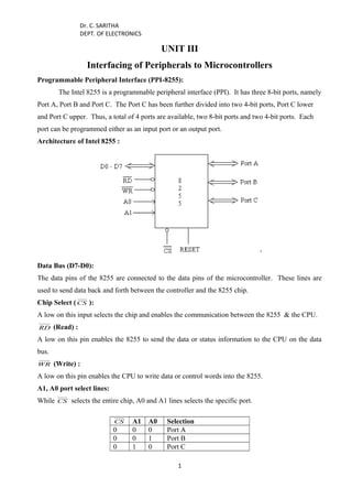
  • 1. Dr. C. SARITHA DEPT. OF ELECTRONICS UNIT III Interfacing of Peripherals to Microcontrollers Programmable Peripheral Interface (PPI-8255): The Intel 8255 is a programmable peripheral interface (PPI). It has three 8-bit ports, namely Port A, Port B and Port C. The Port C has been further divided into two 4-bit ports, Port C lower and Port C upper. Thus, a total of 4 ports are available, two 8-bit ports and two 4-bit ports. Each port can be programmed either as an input port or an output port. Architecture of Intel 8255 : ` Data Bus (D7-D0): The data pins of the 8255 are connected to the data pins of the microcontroller. These lines are used to send data back and forth between the controller and the 8255 chip. Chip Select (CS ): A low on this input selects the chip and enables the communication between the 8255 & the CPU. RD (Read) : A low on this pin enables the 8255 to send the data or status information to the CPU on the data bus. WR (Write) : A low on this pin enables the CPU to write data or control words into the 8255. A1, A0 port select lines: While CS selects the entire chip, A0 and A1 lines selects the specific port. CS A1 A0 Selection 0 0 0 Port A 0 0 1 Port B 0 1 0 Port C 1
  • 2. Dr. C. SARITHA DEPT. OF ELECTRONICS 0 1 1 Control Register 1 x x 8255 is not selected RESET: A high on this pin clears the control register and all ports (A, B & C) are initialized as input ports. PORTA: It is an 8 bit port, can be programmed as either input or output port. It can also be used as a bidirectional port. PORT B: It is an 8 bit port, can be programmed as either input or output port. PORT C: It is an 8 bit port, can be programmed as either input or output port. This port is again divided into two 4-bit ports and each 4 bit port can be programmed individually. Interfacing of 8255 with 8051: In the 8051, Port 0 and Port 2 provide the 16-bit address to access external memory. Among these two ports, P0 provides the lower 8 bit addresses A0-A7 and P2 provides the upper 8 bit addresses A8-A15. More importantly, P0 is also used to provide the 8-bit data bus D0-D7. In other words, pins P0.0 – P0.7 are used for both the address and data paths. This is called address/data multiplexing. To extract the addresses from the P0 pins, keep ALE=1 and connect a 74LS373 D latch to P0. Data lines are directly taken from the P0 by keeping ALE=0 in 8051. Only A1 and A0 lines are used to select the ports of 8255. Fig: Interfacing of 8255 with 8051 2
  • 3. Dr. C. SARITHA DEPT. OF ELECTRONICS As shown in the diagram the P0.0 (A0) and P0.1 (A1) are used to select the ports of 8255 and the remaining lines of P0.2- P0.7(A2-A7) are kept at 0. The P2 lines i.e., P2.0 to P2.6 (A8 to A14) are kept at 0 and the remaining line P2.7 (A15) is connected to the CS line of 8255 through a not gate. The P3.6 (WR ) and P3.7 ( RD) lines of P3 are connected to the WR and RD pins of 8255 respectively. According to the diagram, the addresses of Port A, Port B, Port C and control register are 8000H, 8001H, 8002H and 8003H respectively. By using these addresses a program is written for generating a square wave of 50 % duty cycle using PA0. MOV A,#80H ; Move control word to A MOV DPTR, #8003H ; Load control register address MOVX @DPTR, A ; Issue control word to control register MOV DPTR, #8000H ; DPTR points to Port A START: MOV A, #01H ; A=01H MOVX @DPTR,A ; PA0 =1 ACALL DELAY ; Call a delay for the ON time MOV A,#00H ; A=00H MOVX @DPTR,A ; PA0 = 0 ACALL DELAY ; Call delay for OFF time SJMP START ; Repeat to generate a continuous waveform Interfacing of ADC to the 8051 : An analog to digital converter is used to convert analog signals to digital quantity (binary word). The digital output is fed to the microcontroller for processing. The most popular method of analog to digital conversion is successive approximation method. A widely used ADC chip is ADC0809. Features of ADC 0809: · It is an 8-bit A/D converter with 8 channel analog multiplexer. · It is a National semiconductor make CMOS device. · It uses successive approximation as the conversion technique. · The device operates with single +5V power supply. · The conversion time is 100μs at 640 KHz. · The resolution is 8 bits 3
  • 4. Dr. C. SARITHA DEPT. OF ELECTRONICS · Error is ±1 LSB Interfacing diagram of ADC0809 with 8051: As shown in the diagram Port 1 of 8051 microcontroller is connected to the data lines of ADC0809. The address lines C, B, and A are grounded. So, Channel 0 is selected to apply the analog input. To deactivate the remaining channels, they are grounded. Vref(+), Vcc and OE all are connected to +5V. Vref (-) and GND pins are connected to ground. CLK must be applied to the 10th pin of ADC by using a clock source. SOC line is used to start the conversion and ALE line is used to latch the address. To start the conversion and latch the address make these lines high through the microcontroller. Then conversion begins. After some time EOC line becomes high, to indicate the conversion is completed and the equivalent digital word is at Port 1. The timing diagram shows the entire procedure of analog to digital conversion. Fig: Timing diagram for ADC 0809 4
  • 5. Dr. C. SARITHA DEPT. OF ELECTRONICS Program: START: SETB P3.4 ; Set SOC = 1, ALE = 1 ACALL DELAY ; Call for the delay CLR P3.4 ; Clear SOC and ALE HERE: JNB P3.5,HERE ; Check, for EOC = 1 MOV A, P1 ; Move the data from Port 1 to A SJMP START ; Continue the same Result : Analog input in Volts Digital output in Hex 0 1 2 3 4 5 00 33 66 99 CC FF Interfacing of DAC0800 with 8051 : Digital to analog converters are used to convert digital quantity to analog quantity. D/A converter produces an output proportional to the digital quantity (binary word) applied to its input. A most widely used DAC chip is DAC 0800. Features of DAC0800: · It is an 8-bit DAC · It has fast settling time : 100ns · The conversion technique used is R-2R ladder network method · It operates at +4.5V to +18V supply · Low cost · Full scale error: ±1 LSB · Low power consumption 5
  • 6. Dr. C. SARITHA DEPT. OF ELECTRONICS Interfacing diagram of DAC with 8051: As shown in the diagram Port 1of 8051 microcontroller is connected to the data lines of DAC. The supply V+ is connected to the +5V or +12V. V- is connected to the -12V. The DAC 0800 is a current output device. So, an op-amp is used, to convert the output of DAC i.e., current to voltage. One of the applications of an op amp is as a current to voltage converter. The output of the op amp is the actual analog voltage, which is equivalent to the applied digital word through the microcontroller. Program: START: MOV A, #DATA ; Move the digital input to A MOV P1, A ; Move data 80H to Port 1 SJMP START ; Continue the same Result : Digital input In Hex Analog output In volts 00 40 80 CC FF 0 2.5 5 7.5 10 6
  • 7. Dr. C. SARITHA DEPT. OF ELECTRONICS Digital Data transmission : The transmission of binary data across a link can be accomplished either in parallel mode or serial mode. Parallel transmission : In parallel transmission, multiple bits are sent at a time. The advantage of parallel transmission is speed. But, the disadvantage of this parallel transmission is cost. Because, it requires n channels to transmit n bits. So, Parallel transmission is usually limited to short distances. Examples of parallel transmission include connections between a computer and a printer. Serial transmission : In serial transmission one bit follows another. It needs only one communication channel. The advantage of serial communication is cost. Examples of serial transmission include connections between a computer and a modem using the RS-232 protocol . Serial communication occurs in one of two ways : Asynchronous and Synchronous. 7
  • 8. Dr. C. SARITHA DEPT. OF ELECTRONICS Asynchronous transmission : In asynchronous transmission, the timing of the signal is unimportant. In asynchronous transmission, we send one start bit (0) at the beginning and one or more stop bits (1s) at the end of each byte. There may be a gap between each byte. Synchronous transmission : In synchronous transmission, timing is important. In synchronous transmission, we send bits one after another without start/stop bits or gaps. It is the responsibility of the receiver to group the bits. Serial Communication – Modes : The transmission mode is used to define the direction of signal flow between two devices. There are three types of transmission modes : Simplex, half-duplex and full duplex. Simplex Mode : In simplex mode, the communication is unidirectional, as on a one way street. Only one of the two stations on a link can transmit, the other can only receive. Keyboards and traditional monitors are both examples of simplex devices. The keyboard can only introduce input, the monitor can only accept output. 8
  • 9. Dr. C. SARITHA DEPT. OF ELECTRONICS Half-duplex Mode : In half-duplex mode, each station can both transmit and receive, but not at the same time. When one device is sending, the other can only receive, and vice versa. The half-duplex mode is like a one-lane road with two directional traffic. Walkie-talkies and CB (Citizen’s Band) radios are both half duplex systems. Full-duplex Mode : In full-duplex mode (also called duplex), both stations can transmit and receive simultaneously. The full-duplex mode is like a two way street with traffic flowing in both directions at the same time. One common example of full duplex communication is the telephone network. Serial Communication Protocols : A variety of communication protocols have been developed based on serial communication in the past few decades. Some of them are: 1. RS-232 2. RS-423 3. RS-485 4. RS422 5. USB 6. Fire Wire 7. Ethernet 8. MIDI 9. PCI Express 10. SPI & SCI 11. I2C 12. IrDA 9
  • 10. Dr. C. SARITHA DEPT. OF ELECTRONICS RS-232 – Recommended Standard 232: RS-232 has been a standard for decades as an electrical interface between Data Terminal Equipment (DTE) and Data Circuit-Terminating Equipment (DCE). A DTE is any device that is source or destination for binary data. A DCE is any device that transmits or receives data in the form of an analog or digital signal through a network. RS-232 is the oldest and most popular serial communication standard. RS232 stands for Recommended Standard number 232. It is developed by EIA (Electronics Industries Association) in 1960. It is the standard used in PCs and various types of equipment. It is used to connect only two devices. This RS232 standard defines the interface as a 25 wire cable with male and a female DB 25 pin connector attached to either end. The length of the cable may not exceed 15 meters (50 feet). However, since the standard was set long before the advent of TTL logic family, its input and output voltage level are not TTL compatible. In RS232, a 1 bit is represented by -3 to -15V, while a 0 bit is represented by +3 to +15V, making -3 to +3 undefined. For this reason, to connect any RS232 to a microcontroller system , we must use voltage converters such as MAX 232 to convert the TTL logic levels to the RS232 voltage level, and vice-versa. 8051 connection to RS232 : The 8051 has two pins that are used specifically for transferring and receiving data serially. These two pins are called TxD and RxD and are part of the port 3 (P3.0 and P3.1). Pin 11 of the 8051 (P3.1) is assigned to TxD and pin 10 (P3.0) is designated as RxD. These pins are TTL compatible. Therefore, they require line driver to make them RS232 compatible. One such line driver is the MAX232 chip. 10
  • 11. Dr. C. SARITHA DEPT. OF ELECTRONICS The MAX232 has two sets of line drivers for transferring and receikving data. The line drivers used for TxD are called T1 and T2, while the line drivers for RxD are designated as R1 and R2. In many applications only one set is used. For example, T1 and R1 are used together for TxD and RxD of the 8051, and the second set is left unused. In MAX232 the T1 line driver has a designation of T1 in and T1 out on pin numbers 11 and 14, respectively. The T1 in pin is the TTL side and is connected to TxD of the microcontroller, while T1 out is the RS 232 side that is connected to the RxD pin of the RS232 DB connector. The R1 line driver has a designation of R1 in and R1 out on pin numbers 13 and 12 respectively. The R1 in (pin 13) is the RS232 side that is connected to the TxD pin of the RS232 DB connector, and R1 out (pin 12) is the TTL side that is connected to the RxD pin of the microcontroller. RS-485 : RS-485 is an improved RS-422 with the capability to connect up to 16 devices (transceivers) on one serial bus to form a network. Such a network can have a "daisy chain" topology where each device is connected to two other devices except for the devices on the ends. Only one device may drive data onto the bus at a time. The standard does not specify the rules for deciding who transmits and when on such a network. That is up to the system designer to define. RS-423 : RS-423 is similar to RS-232C except that it allows for higher baud rates and longer cable lengths because it tolerates ground voltage differences between sender and receiver. The maximum signal voltage levels are ±6 volts. Ground voltage differences can occur in electrically noisy environments where heavy electrical machinery is operating. RS-422 : RS-422, like RS-232, is used to connect only two systems. It uses differential, or "double ended" data transmission, which means that data is transmitted simultaneously on two wires between two stations independent of the ground wire. Each signal requires 2 wires with a ground present in the system. The advantage of this method over RS-232 is higher speeds and longer cable lengths - 4000 feet at a 100K baud rate, for example. 11
  • 12. Dr. C. SARITHA DEPT. OF ELECTRONICS SPI – Serial Peripheral Interface: It is a three-wire based communication system. One wire each for Master to slave and Vice-versa, and one for clock pulses. There is an additional SS (Slave Select) line, which is mostly used when we want to send/receive data between multiple ICs. I2C – Inter-Integrated Circuit: Pronounced eye-two-see or eye-square-see, this is an advanced form of USART. The transmission speeds can be as high as a whopping 400KHz. The I2C bus has two wires – one for clock, and the other is the data line, which is bi-directional – this being the reason it is also sometimes (not always – there are a few conditions) called Two Wire Interface (TWI). It is a pretty new and revolutionary technology invented by Philips. FireWire : Developed by Apple, they are high-speed buses capable of audio/video transmission. The bus contains a number of wires depending upon the port, which can be either a 4-pin one, or a 6-pin one, or an 8-pin one. Ethernet: Used mostly in LAN connections, the bus consists of 8 lines, or 4 Tx/Rx pairs. Universal serial bus (USB): This is the most popular of all. Is used for virtually all type of connections. The bus has 4 lines: VCC, Ground, Data+, and Data-. ××××× 12