This document summarizes research optimizing the threshold voltage (VTH) for a 65nm PMOS transistor using Silvaco TCAD simulation tools. The researchers varied three fabrication factors - gate oxide thickness, channel doping concentration, and channel implantation concentration - in the simulation. The simulation results showed a VTH value of -2.55427V for a 65nm PMOS transistor with a gate oxide thickness of 0.0025um, boron channel doping of 2x10¹⁵, and phosphorus implantation of 3.5x10¹³ atom/cm-1. Thicker gate oxides, higher channel doping, and increased implantation concentrations each caused higher VTH values in the simulation, consistent with theoretical expectations.
Performance Comparison of CMOS and Finfet Based Circuits At 45nm Technology U...IJERA Editor
According to the Moore’s Law, the number of transistors in a unit chip area double every two years. But the existing technology of integrated circuit formation is posing limitations to this law. CMOS technology shows certain limitations as the device is reduced more and more in the nanometer regime out of which power dissipation is an important issue. FinFET is evolving to be a promising technology in this regard. This paper aims to analyze and compare the characteristics of CMOS and FinFET circuits at 45nm technology. Inverter circuit is implemented in order to study the basic characteristics such as voltage transfer characteristics, leakage current and power dissipation. Further the efficiency of FinFET to reduce power as compared to CMOS is proved using SRAM circuit. The results show that the average power is reduced by 92.93% in read operation and by 97.8% in write operation.
Implementation of Three phase SPWM Inverter with Minimum Number of Power Elec...IJMTST Journal
In the past decades, the researchers have dealt with the conventional topology, which possesses sum switches of Multilevel Inverter is applied to PWM method. The present research work has been introduced a new method of multilevel inverter using reduced switches is applied with PWM technique. In introduction part the conventional new multilevel inverter & switching pattern are explained. In second part PWM technique of proposed work and circuits is explained. The width of this pulses are modulated in order to obtain inverter output voltage control and to reduce its harmonic content. Sinusoidal pulse width modulation or SPWM is the most common method in motor control and inverter application. Conventionally, to generate the signal, triangle wave as a carrier signal is compared with the sinusoidal wave, whose frequency is the desired frequency.
DESIGN OF A HIGH PRECISION, WIDE RANGED ANALOG CLOCK GENERATOR WITH FIELD PRO...VLSICS Design
This paper presents a circuit of a high-precision, wide ranged, analog clock generator with on-chip programmability feature using Floating-gate transistors. The programmable oscillator can attain a continuous range of time-periods lying in the programming precision range of Floating Gates. The circuit consists of two sub circuits: Current Generator circuit and Wave Generator circuit. The current of current generator circuit is programmable and mirrored to the wave generator to generate the desired square wave. The topology is well suited to applications like clocking high performance ADCs and DACs as well as used as the internal clock in structured analog CMOS designs. A simulation model of the circuit was built in T-Spice, 0.35µm CMOS process. The circuit results in finely tuned clock with programmability precision of about 13bit [1]. Simulation results show high amount of temperature insensitivity (0.507ns/°C) for a large range of thermal conditions. The proposed circuit can compensate any change in temperature. The circuit design can be operated at low supply voltage i.e., 1v.
High Performance and Low power VLSI CMOS Circuit Designs using ONOFIC Approach IJERA Editor
Leakage power dissipation a major concern for scaling down portable devices. Improving high performance with reduced power consumption and chip area are the main constraint for designing VLSI CMOS circuits. In this paper, high performance and low power ONOFIC approach for VLSI CMOS circuits have been implemented. Mostly the concentrated part in deep sub micron regime is the power dissipation. Many techniques have been proposed for reducing leakage current in deep sub micron but with some limitations they are not suitable for actual requirements. Here we discussed two techniques named LECTOR & ONOFIC. The proposed On/Off Logic (ONOFIC) serves the needs for deep sub micron with its reduced power dissipation and increased performance in VLSI circuits. Thus the proposed ONOFIC approach results have been compared with the LECTOR technique and observed that the proposed technique improves the performance and reduce the power dissipation.
Implementation of d space controlled dpwm basedeSAT Journals
Abstract The paper presents dSPACE controlled Induction motor drive fed through Discontinuous pulse width modulation (DPWM) algorithm based voltage source inverter. Two important performance measuring factors harmonic distortion in line current and dc bus utilization of the inverter can be improved with Discontinuous PWM approach in comparison with the popular conventional space vector (CSVPWM) approach; the paper contemplates on the implementation of DPWM algorithm for pulse generation which in turn are fed to intelligent power module that feeds the motor drive through DS1104 PPC603e / 250 MHz control desk. The results conclude the successful implementation of dSPACE Controlled induction motor drive. To validate the proposed work, numerical simulation including the experimental results is presented. Keywords:-DPWM, dSPACE, RTI
In this paper VLSI design have been introduce decrease the area and power CMOS 90 nm technology is used for designing nor gate. The power consumption and area of nor gate compared in this paper. The proposed design reduces the power consumption and area. The nor gate reduces power consumption by 46% and area by 67% .two design flow are implement, fully automatic and semicustom .the semicustom design better than fully automatic because in this design flow modification is done to minimize the power and area.
Design and Simulation of a soft switching scheme for a dc-dc Boost Converter ...CSCJournals
This paper presents the design of simple but powerful soft switching scheme for a DC-DC Boost Converter with a closed loop control. A new novel soft switching scheme is proposed with a single switch and minimum components which offers load independent operations. The only switch used in this converter is switched ON at zero current and switched OFF at zero voltage .The proposed Controller is used to improve the dynamic performance of DC-DC converter by achieving a robust output voltage against load disturbances. The duty cycle of the Boost converter is controlled by PI Controller. A 50W/50KHz soft switched PWM Boost converter is simulated and analyzed. The results are simulated using PSIM
Performance Improvement of Multi Level Inverter fed Vector Controlled Inducti...IJPEDS-IAES
In this paper, the analysis of space vector based multi level inverter (MLI) fed vector controlled induction motor drive for a low speed operation is presented. The performance of indirect field oriented controlled induction motor drive (IMD) is poor with two-level inverter for low speed operations (LSO). The reduction in performance and peak value of torque are mainly due to the non-linearity caused by stator voltage drop and inverter. Hence the performance factors of induction motor drive are analyzed with the multi level inverters under different operating conditions. In this approach, the steady state ripple content in the current and torque waveforms are reduced and that to ripple content of torque is reduced from 0.15 to 0.05 under steady state with five-level inverter. When there is a step change in the load torque, the momentary decrease in speed with five-level inverter is less when compared two and three-level inverters and the speed response reaches the reference value very quickly with five-level inverter during steady state and transient periods. So the overall performance of drive is improved with five- level inverter when compared to two-level and three- level inverters under low speed operations.
IJRET : International Journal of Research in Engineering and Technology is an international peer reviewed, online journal published by eSAT Publishing House for the enhancement of research in various disciplines of Engineering and Technology. The aim and scope of the journal is to provide an academic medium and an important reference for the advancement and dissemination of research results that support high-level learning, teaching and research in the fields of Engineering and Technology. We bring together Scientists, Academician, Field Engineers, Scholars and Students of related fields of Engineering and Technology
Synchronous flyback converter with synchronous buck post regulatoreSAT Publishing House
IJRET : International Journal of Research in Engineering and Technology is an international peer reviewed, online journal published by eSAT Publishing House for the enhancement of research in various disciplines of Engineering and Technology. The aim and scope of the journal is to provide an academic medium and an important reference for the advancement and dissemination of research results that support high-level learning, teaching and research in the fields of Engineering and Technology. We bring together Scientists, Academician, Field Engineers, Scholars and Students of related fields of Engineering and Technology
Low Power Design of Standard Digital Gate Design Using Novel Sleep Transisto...IJMER
In the nanometer range design technologies static power consumption is very important
issue in present peripheral devices. In the CMOS based VLSI circuits technology is scaling towards
down in respect of size and achieving higher operating speeds. We have also considered these
parameters such that we can control the leakage power. As process model design are getting smaller
the density of device increases and threshold voltage as well as oxide thickness decrease to maintain
the device performance. In this article two novel circuit techniques for reduction leakage current in
NAND and NOR inverters using novel sleepy and sleepy property are investigated. We have proposed a
design model that has significant reduction in power dissipation during inactive (standby) mode of
operation compared to classical power gating methods for these circuit techniques. The proposed
circuit techniques are applied to NAND and NOR inverters and the results are compared with earlier
inverter leakage minimization techniques. All low leakage models of inverters are designed and
simulated in Tanner Tool environment using 65 nm CMOS Technology (1volt) technologies. Average
power, Leakage power, sleep transistor
Comparative Study of Fuzzy Logic Based Speed Control of Multilevel Inverter f...IJPEDS-IAES
This paper presents a comparative analysis of speed control of brushless DC motor (BLDC) drive fed with conventional two-level, three and five level diode clamped multilevel inverter (DC-MLI). The performance of the drive system is successfully evaluated using Fuzzy Logic (FL) based speed controller. The control structure of the proposed drive system is described. The speed and torque characteristic of conventional two-level inverter is compared with the three and five-level multilevel inverter (MLI) for various operating conditions. The three and five level diode clamped multilevel inverters are simulated using IGBT’s and the mathematical model of BLDC motor has been developed in MATLAB/SIMULINK environment. The simulation results show that the Fuzzy based speed controller eliminate torque ripples and provides fast speed response. The developed Fuzzy Logic model has the ability to learn instantaneously and adapt its own controller parameters based on disturbances with minimum steady state error, overshoot and rise time of the output voltage.
Dual inverter fed induction motor drives provide more advantages in contrast with other multilevel inverter drives. Coupled PWM techniques provide good standard of output voltage than the decoupled PWM techniques for dual inverter configuration. In this paper analysis of open end winding induction motor by coupled random PWM signals and decoupled SVPWM signals was carried out. Induction motor by random PWM technique generate low acoustic noise and electromagnetic interference to near by systems. The performance evaluation of the drive wss implemented in MATLAB/simulink and the results were presented.
IJRET : International Journal of Research in Engineering and Technology is an international peer reviewed, online journal published by eSAT Publishing House for the enhancement of research in various disciplines of Engineering and Technology. The aim and scope of the journal is to provide an academic medium and an important reference for the advancement and dissemination of research results that support high-level learning, teaching and research in the fields of Engineering and Technology. We bring together Scientists, Academician, Field Engineers, Scholars and Students of related fields of Engineering and Technology
Design & characterization of high speed power efficient cmos comparatorIAEME Publication
In this paper authors have design the High Speed Power Efficient CMOS Voltage
Comparator which can be realized in A/D Converters. The simulation is carried out in 130nm
and 90nm technologies. The supply voltage for this comparator is 1v and 0.9v for 130nm and
90nm respectively. The Characterization of comparator is done in terms of offset, ICMR,
propagation delay, power dissipation in both the technologies and the result has been
compared for both the technologies. The simulation results shows that the speed of 1.92GHz
and 2.44GHz with the power dissipation of 9.19µW and 7.45µW was achieved in 130nm and
90nm technologies respectively.
Robust vibration control at critical resonant modes using indirect-driven sel...ISA Interchange
This paper presents an improved indirect-driven self-sensing actuation circuit for robust vibration control of piezoelectrically-actuated flexible structures in mechatronic systems. The circuit acts as a high-pass filter and provides better self-sensing strain signals with wider sensing bandwidth and higher signal-to-noise ratio. An adaptive non-model-based control is used to compensate for the structural vibrations using the strain signals from the circuit. The proposed scheme is implemented in a PZT-actuated suspension of a commercial dual-stage hard disk drive. Experimental results show improvements of 50% and 75% in the vibration suppression at 5.4kHz and21 kHz respectively, compared to the conventional PI control.
International Journal of Engineering Research and Applications (IJERA) is an open access online peer reviewed international journal that publishes research and review articles in the fields of Computer Science, Neural Networks, Electrical Engineering, Software Engineering, Information Technology, Mechanical Engineering, Chemical Engineering, Plastic Engineering, Food Technology, Textile Engineering, Nano Technology & science, Power Electronics, Electronics & Communication Engineering, Computational mathematics, Image processing, Civil Engineering, Structural Engineering, Environmental Engineering, VLSI Testing & Low Power VLSI Design etc.
Ultra-low power 0.45 mW 2.4 GHz CMOS low noise amplifier for wireless sensor ...journalBEEI
This paper describes the design topology of a ultra-low power low noise amplifier (LNA) for wireless sensor network (WSN) application. The proposed design of ultra-low power 2.4 GHz CMOS LNA is implemented using 0.13-μm Silterra technology. The LNA benefits of low power from forward body bias technique for first and second stages. Two stages are implemented in order to enhance the gain while obtaining low power consumption for overall circuit. The simulation results show that the total power consumed is only 0.45 mW at low supply voltage of 0.55 V. The power consumption is decreased about 36% as compared with the previous work. A gain of 15.1 dB, noise figure (NF) of 5.9 dB and input third order intercept point (IIP3) of -2 dBm are achieved. The input return loss (S11) and the output return loss (S22) is -17.6 dB and -12.3 dB, respectively. Meanwhile, the calculated figure of merit (FOM) is 7.19 mW-1.
Ground Bounce Noise Reduction in Vlsi CircuitsIJERA Editor
Scaling of devices in CMOS technology leads to increase in parameter like Ground bounce
noise, Leakage current, average power dissipation and short channel effect. FinFET are the promising substitute
to replace CMOS. Ground bounce noise is produced when power gating circuit goes from SLEEP to ACTIVE
mode transition. FinFET based designs are compared with MOSFET based designs on basis of different
parameter like Ground bounce noise, leakage current and average power dissipation. HSPICE is the software
tool used for simulation and circuit design.
Various and multilevel of wavelet transform for classification misalignment o...TELKOMNIKA JOURNAL
Induction motors have become a major part of the industry because of strong construction, cheap in purchasing and maintenance, high efficiency, and easy to operate. Preventive maintenance must always be carried out on all industrial equipment, including induction motors to last long and prevent further damage. Based on research in the industry, around 42%-50% or almost 50% is bearing damage. One reason is the occurrence of misalignment during the installation of the load on the induction motor. This study tries to identify the condition of the motor and classify the level of misalignment damage that occurs. In the process, the mother wavelet like as Daubechis, Symlet and Coiflet discrete wavelet transform (DWT) are selected as tools in processing motor vibration data. The level of DWT applied is 1st to 3rd level. Then, the three types of signal extraction, namely sum, range, and energy, which are obtained from a high-frequency signal of DWT, are used as input to Quadratic and Linear Discriminant Analysis. Then, discriminant analysis analyzes and classifies them into normal operation and two misalignments conditions. The simulation shows that 1st level of Daubechis DWT combined with quadratic discriminant analysis generates the best classification. It results 0% error of classification with Db3, Db4 and Db5, 4.17% error with Db1 and 8.33% error with Db2.
Effect of fiber and solenoid variation parameters on the elements of a correc...IJECEIAES
Controlling the polarization of the light output from single-mode fiber systems is very important for connecting it to polarization-dependent integrated optical circuits, while applications using a heterodyne detection system. Polarization controller using fiber squeezer is attractive for a lowloss, low-penalty coherent optical fiber trunk system. However, for polarization controllers using electromagnetic fiber squeezer, the stability problem due to the saturation of their magnetic circuit must be studied. In fact, in their conventional configuration, open-loop stability affects performance and limits applications. First at all, this effect has been analyzed and a feedback circuit with correctors has been proposed to improve stability performance. Then a simulation study is proposed to examine the influence of the system parameters on the corrector constants. The results of the simulation show that if the system parameters change the constants Kp, Ki and Kd of the PID corrector must be adjusted to keep an optimized dynamic response.
IOSR Journal of Humanities and Social Science is an International Journal edited by International Organization of Scientific Research (IOSR).The Journal provides a common forum where all aspects of humanities and social sciences are presented. IOSR-JHSS publishes original papers, review papers, conceptual framework, analytical and simulation models, case studies, empirical research, technical notes etc.
Synthesis and structural characterization of Al-CNT metal matrix composite us...IOSR Journals
In the present study Carbon nanotube(CNT) reinforced (Al) composite was synthesized by physical mixing method and CNT’s distribution within the matrix was traced and characterized. Ultrasonication was used to disperse the CNTs in Al nano powder followed by magnetic stirring. Samples of different weight percentage of CNT(0.5wt %, 1wt %, 1.5wt %, 2wt % of CNT) were obtained using this technique. Stuructural characteristics of the samples were explored using X-Ray diffraction(XRD),Scanning Electronic Microscope(SEM) and Transmission Electronic Microscope(TEM) technologies. Uniform distribution of CNTs within the matrix and the strength of metal/CNT interface were confirmed from SEM and TEM images. Along with the distribution of CNTs, XRD also validates the phase composition of the composite.
IOSR Journal of Electronics and Communication Engineering(IOSR-JECE) is an open access international journal that provides rapid publication (within a month) of articles in all areas of electronics and communication engineering and its applications. The journal welcomes publications of high quality papers on theoretical developments and practical applications in electronics and communication engineering. Original research papers, state-of-the-art reviews, and high quality technical notes are invited for publications.
Abstract: While designing a cellular network, the main issue for the network planning is to achieve maximum
capacity while maintaining an acceptable grade of service and good speech quality. Planning an immature
network does not allow future growth and expansion. Wise & calculative re-use of site location in the future
network structure will save money for the operator. For this reason, digital maps are one of the most essential
elements to the network engineers while they have to think about expanding their business. However, the digital
maps cost a lot of money. This problem can be mitigated if Google Earth is used.
In this paper, the procedure of how to design a cellular digitized map on Google Earth is shown. By
calculating the cell radius, implementing the single cell site, forming the 7-cell cluster and all the cells a low
cost digitized map is designed. It is necessary to have a digitized map in mobile communication because
ultimate goal includes efficient usage of RF wave, frequency reuse, total use of BW and last but not the least
cost reduction.
Keywords: Cellular digitized map, Cell radius, Google Earth.
IOSR Journal of Mechanical and Civil Engineering (IOSR-JMCE) is an open access international journal that provides rapid publication (within a month) of articles in all areas of mechanical and civil engineering and its applications. The journal welcomes publications of high quality papers on theoretical developments and practical applications in mechanical and civil engineering. Original research papers, state-of-the-art reviews, and high quality technical notes are invited for publications.
Design analysis and Commissioning Of High Mast Lighting PolesIOSR Journals
Along a major highway, luminaire pole structures may be seen every 101 of a mile.From documented
cases, it appears that these structures started to experience fatigue problems in the last three decades. The
general public might not be aware of the problem, because if such a failure occurs, the structure is replaced.
Those working in the fatigue area realize that this issue is a serious matter[15][16]. Clearly, the damage is
costly, costing up to thousands of dollars per occurrence. For this purpose, a high mast lighting poles are
fabricated using steel due to its high strength, ductilityproperty and wear resistance. The high mast structure
(HMS) has the characters of light weight and high cost efficiency. It possess large ratio of height (H) to least
horizontal dimension (D) that makes it more slender and wind-sensitive than any other structures[17].
Therefore, the purpose of this research is to design optimal high mast poles taking into account its specification,
environmental conditions for placement and economy. Initially, among various pole designs, the high mast pole
is considered to be in tapered section as it is more reliable and economical. Then, analysis is performed in solid
works by keeping the base section to be fixed and applying compressive load on the top section of the pole due
to heavy weight of cantilever mast arm and luminaire. This project illustrates the theoretical basis and the
analytical development of the high mast lighting poles
The effect of rotational speed variation on the velocity vectors in the singl...IOSR Journals
The current investigation is aimed to simulate the three-dimensional complex internal flow in a
centrifugal pump impeller with five twisted blades by using a specialized computational fluid dynamics (CFD)
software ANSYS /FLUENT 14code with a standard k-ε two-equation turbulence model.
A single blade passage will be modeled to give more accurate results for velocity vectors on (blade, hub, and
shroud). The potential consequences of velocity vectors associated with operating a centrifugal compressor in
variable rotation speed.
A numerical three-dimensional, through flow calculations to predict velocity vectors through a
centrifugal pump were presented to examined the effect of rotational speed variation on the velocity vectors of
the centrifugal pump . The contours of the velocity vectors of the blade, hub, and shroud indicates low velocity
vectors in the suction side at high rotational speed (over operation limits )and the velocity vectors increases
gradually until reach maximum value at the leading edge (2.63×10 m/s) of the blade
Stress Analysis of Automotive Chassis with Various ThicknessesIOSR Journals
Abstract : This paper presents, stress analysis of a ladder type low loader truck chassis structure consisting of
C-beams design for application of 7.5 tonne was performed by using FEM. The commercial finite element
package CATIA version 5 was used for the solution of the problem. To reduce the expenses of the chassis of the
trucks, the chassis structure design should be changed or the thickness should be decreased. Also determination
of the stresses of a truck chassis before manufacturing is important due to the design improvement. In order to
achieve a reduction in the magnitude of stress at critical point of the chassis frame, side member thickness,
cross member thickness and position of cross member from rear end were varied. Numerical results showed that
if the thickness change is not possible, changing the position of cross member may be a good alternative.
Computed results are then compared to analytical calculation, where it is found that the maximum deflection
agrees well with theoretical approximation but varies on the magnitude aspect.
Keywords - Stress analysis, fatigue life prediction and finite element method etc.
Documentaries use for the design of learning activitiesIOSR Journals
Abstract: Documentaries used in the training field constitute the rich sources of information. They have the
advantage to associate the elements of knowledge with events which request the episodic memory of the
learner.Thus, these documentaries increase the probability of retention of knowledge they convey. However, the
logical sequence of knowledge does not guarantee an efficient construction which can be mobilized in situations
of action. In this paper, we seek how to benefit from the potential of these documentaries to promote the
construction and mobilization of knowledge by the learner in an elearning platform. Particularly, we propose a
method allowing segmenting the contents of a documentary to design learning activities. Based on a case study
related to the field of mechatronics, we begin by segmenting the content of a documentary in terms of elements
of knowledge (facts, concepts, procedures, and rules) then we connect with each of these problems they seek to
find answers. We reorganize learning activities to promote the acquisition and mobilization of knowledge by the
learner. We conclude by proposing a pedagogical scenario to implement these activities in elearning platform.
Keywords: LMS, IMS-LD, Documentary, Design, Elearning
IOSR Journal of Business and Management (IOSR-JBM) is an open access international journal that provides rapid publication (within a month) of articles in all areas of business and managemant and its applications. The journal welcomes publications of high quality papers on theoretical developments and practical applications inbusiness and management. Original research papers, state-of-the-art reviews, and high quality technical notes are invited for publications.
IOSR Journal of Mathematics(IOSR-JM) is an open access international journal that provides rapid publication (within a month) of articles in all areas of mathemetics and its applications. The journal welcomes publications of high quality papers on theoretical developments and practical applications in mathematics. Original research papers, state-of-the-art reviews, and high quality technical notes are invited for publications.
Analysis of Commutation Torque Ripple Minimization for Brushless DC Motor Bas...IJERA Editor
Brushless DC Motors (BLDCM) are widely used in automated industrial applications like Computer Numerical Control (CNC) machinery, aerospace applications and in the field of robotics.But it still suffers from commutation torque which mainly depends on speed and transient line commutation interval. BLDC MOTOR torque ripple causes increased acoustic noise and undesirable speed fluctuation. This paper presents a new circuit topology and dc link voltage current in the control strategy to keep incoming and outgoing phase currents changing at the same rate during commutation. In this paper dc-dc single ended primary inductor converter (SEPIC) a switch selection circuit are employed in front of inverter. In order to obtain the desired commutation voltage resulting in reduced commutation torque ripple. Compared with simulation result conventional system and proposed method can obtain desired voltage much faster and minimize commutation torque ripple more efficiently
High performance novel dual stack gating technique for reduction of ground bo...eSAT Journals
Abstract The development of digital integrated circuits is challenged by higher power consumption. The combination of higher clock speeds, greater functional integration, and smaller process geometries has contributed to significant growth in power density. Today leakage power has become an increasingly important issue in processor hardware and software design. So to reduce the leakages in the circuit many low power strategies are identified and experiments are carried out. But the leakage due to ground connection to the active part of the circuit is very higher than all other leakages. As it is mainly due to the back EMF of the ground connection we are calling it as ground bounce noise. To reduce this noise, different methodologies are designed. In this paper, a number of critical considerations in the sleep transistor design and implementation includes header or footer switch selection, sleep transistor distribution choices and sleep transistor gate length, width and body bias optimization for area, leakage and efficiency. Novel dual stack technique is proposed that reduces not only the leakage power but also dynamic power. The previous techniques are summarized and compared with this new approach and comparison of both the techniques is done with the help of Digital Schematic( DSCH ) and Microwind low power tools. Stacking power gating technique has been analyzed and the conditions for the important design parameters (Minimum ground bounce noise) have been derived. The Monte-Carlo simulation is performed in Microwind to calculate the values of all the needed parameters for comparison. Index Terms: Ground Bounce Noise ,Power gating schemes ,Static power dissipation, Dynamic power dissipation, Power gating parameters, Sleep transistors, Novel dual stack approach, Transistor leakage power
A low-power 2-bit/step operation technique is proposed which uses dynamic threshold configuring comparator instead of multiple digital-to-analog converters (DACs). Power and area overhead is minimized by successively activated comparators. The comparator threshold is configured by simple Vcm biased current source, which keep the ADC free from power supply variations over 10%. To implement power efficient and high performance analog-to-digital converters the designers are urged to design an optimized dual tail comparator. In this paper, It is shown that in the proposed dual tail comparator both the power and delay time is significantly reduced.
Design and performance analysis of low phase noise LC-voltage controlled osci...TELKOMNIKA JOURNAL
Voltage controlled oscillator (VCO) offers the radio frequency (RF) system designer a freedom to select the required frequency. Today’s wireless communication system imposes a very stringent requirement in terms of phase noise generated in VCO. This study presents an inductive source degeneration technique to improve the phase noise performance of the inductance-capacitance (LC)-VCO. Double cross-coupled topology has been chosen for the proposed VCO. The post layout simulations with the parasitic resistance, inductance, capacitance (RLC) extracted view is carried out with united microelectronics corporations (UMC) 0.18 µm process by spectre simulator of cadence tools. The proposed VCO provides a phase noise
of -124.3 dBc/Hz @ 1 MHz. The tuning range obtained is 19.87% with a centre frequency of 2.46 GHz which makes it suitable for industrial, scientific, and medical (ISM) band applications. It consumes a power of 2.10 mW. Also, a good figure of merit of -189 is achieved. The total layout area occupied is 477×545 µm2.
International Journal of Engineering Research and Applications (IJERA) is an open access online peer reviewed international journal that publishes research and review articles in the fields of Computer Science, Neural Networks, Electrical Engineering, Software Engineering, Information Technology, Mechanical Engineering, Chemical Engineering, Plastic Engineering, Food Technology, Textile Engineering, Nano Technology & science, Power Electronics, Electronics & Communication Engineering, Computational mathematics, Image processing, Civil Engineering, Structural Engineering, Environmental Engineering, VLSI Testing & Low Power VLSI Design etc.
Analysis of leakage current calculation for nanoscale MOSFET and FinFETIJTET Journal
Abstract—This paper presents logic level estimators of leakage current for nanoscale digital standard cell circuits. Here the proposed estimation model is based on the characterization of internal node voltages of cells and the characterization of leakage current in a single Field-Effect Transistor (FET). Finally the estimation model allowed direct implementation of supply voltage variation impact on leakage current and output voltage drop (loading effect).The technique is feasible for implementation in Hardware Description Language (HDL) and HDL cell models supporting leakage estimation at simulation time.
EVALUATION OF OPTICALLY ILLUMINATED MOSFET CHARACTERISTICS BY TCAD SIMULATIONVLSICS Design
In this paper we report effect of optical illumination on Silicon MOSFET. The MOSFET has been studied in respect of current voltage, transconductance admittance and scattering parameters. Gain analysis of the Silicon MOSFET is done in dark and under optical illumination. The device is fabricated using ATHENA™ process simulator and the device simulation is performed using ATLAS™ from SILVACO international. The simulation results indicate potential of MOSFET as optically sensitive structure which can be used for increase in data transmission/reception rates, reduction of interconnect delays, elimination of clock skew, or as a photodetector for optoelectronic applications at low and radio frequency.
EVALUATION OF OPTICALLY ILLUMINATED MOSFET CHARACTERISTICS BY TCAD SIMULATIONVLSICS Design
In this paper we report effect of optical illumination on Silicon MOSFET. The MOSFET has been studied in
respect of current voltage, transconductance admittance and scattering parameters. Gain analysis of the
Silicon MOSFET is done in dark and under optical illumination. The device is fabricated using ATHENA™
process simulator and the device simulation is performed using ATLAS™ from SILVACO international.
The simulation results indicate potential of MOSFET as optically sensitive structure which can be used
for increase in data transmission/reception rates, reduction of interconnect delays, elimination of clock
skew, or as a photodetector for optoelectronic applications at low and radio frequency.
Circulating current suppression and natural voltage balancing using phase-shi...IJECEIAES
The challenge of achieving a balanced capacitor voltage is one of the factors affecting the efficient operation of modular multilevel converters (MMC). This paper investigates this challenge through a proposed method that utilizes a high carrier frequency phase-shifted pulse width modulation (PS-PWM) scheme. This method aims to achieve natural balancing without the need for any additional control mechanisms. Moreover, the number of output voltage levels is affected by the phase shift between the carriers of the upper and lower arms. When there is no phase shift, N+1 discrete levels are achieved, but when there is a phase shift, the number of discrete levels increases to 2N+1. The proportional-resonant (PR) controller and moving average filter (MAF) are employed to decrease the capacitor voltage ripples by suppressing the fourth and second harmonics in the circulating currents. The MMC inverter structure is modeled and simulated in the PLECS and MATLAB/Simulink environments to evaluate the impact of this control scheme on the converter’s performance.
Analysis of CMOS Comparator in 90nm Technology with Different Power Reduction...IJECEIAES
To reduce power consumption of regenerative comparator three different techniques are incorporated in this work. These techniques provide a way to achieve low power consumption through their mechanism that alters the operation of the circuit. These techniques are pseudo NMOS, CVSL (cascode voltage switch logic)/DCVS (differential cascode voltage switch) & power gating. Initially regenerative comparator is simulated at 90 nm CMOS technology with 0.7 V supply voltage. Results shows total power consumption of 15.02 µW with considerably large leakage current of 52.03 nA. Further, with pseudo NMOS technique total power consumption increases to 126.53 µW while CVSL shows total power consumption of 18.94 µW with leakage current of 1270.13 nA. More then 90% reduction is attained in total power consumption and leakage current by employing the power gating technique. Moreover, the variations in the power consumption with temperature is also recorded for all three reported techniques where power gating again show optimum variations with least power consumption. Four more conventional comparator circuits are also simulated in 90nm CMOS technology for comparison. Comparison shows better results for regenerative comparator with power gating technique. Simulations are executed by employing SPICE based on 90 nm CMOS technology.
Immunizing Image Classifiers Against Localized Adversary Attacksgerogepatton
This paper addresses the vulnerability of deep learning models, particularly convolutional neural networks
(CNN)s, to adversarial attacks and presents a proactive training technique designed to counter them. We
introduce a novel volumization algorithm, which transforms 2D images into 3D volumetric representations.
When combined with 3D convolution and deep curriculum learning optimization (CLO), itsignificantly improves
the immunity of models against localized universal attacks by up to 40%. We evaluate our proposed approach
using contemporary CNN architectures and the modified Canadian Institute for Advanced Research (CIFAR-10
and CIFAR-100) and ImageNet Large Scale Visual Recognition Challenge (ILSVRC12) datasets, showcasing
accuracy improvements over previous techniques. The results indicate that the combination of the volumetric
input and curriculum learning holds significant promise for mitigating adversarial attacks without necessitating
adversary training.
Courier management system project report.pdfKamal Acharya
It is now-a-days very important for the people to send or receive articles like imported furniture, electronic items, gifts, business goods and the like. People depend vastly on different transport systems which mostly use the manual way of receiving and delivering the articles. There is no way to track the articles till they are received and there is no way to let the customer know what happened in transit, once he booked some articles. In such a situation, we need a system which completely computerizes the cargo activities including time to time tracking of the articles sent. This need is fulfilled by Courier Management System software which is online software for the cargo management people that enables them to receive the goods from a source and send them to a required destination and track their status from time to time.
Welcome to WIPAC Monthly the magazine brought to you by the LinkedIn Group Water Industry Process Automation & Control.
In this month's edition, along with this month's industry news to celebrate the 13 years since the group was created we have articles including
A case study of the used of Advanced Process Control at the Wastewater Treatment works at Lleida in Spain
A look back on an article on smart wastewater networks in order to see how the industry has measured up in the interim around the adoption of Digital Transformation in the Water Industry.
Democratizing Fuzzing at Scale by Abhishek Aryaabh.arya
Presented at NUS: Fuzzing and Software Security Summer School 2024
This keynote talks about the democratization of fuzzing at scale, highlighting the collaboration between open source communities, academia, and industry to advance the field of fuzzing. It delves into the history of fuzzing, the development of scalable fuzzing platforms, and the empowerment of community-driven research. The talk will further discuss recent advancements leveraging AI/ML and offer insights into the future evolution of the fuzzing landscape.
Explore the innovative world of trenchless pipe repair with our comprehensive guide, "The Benefits and Techniques of Trenchless Pipe Repair." This document delves into the modern methods of repairing underground pipes without the need for extensive excavation, highlighting the numerous advantages and the latest techniques used in the industry.
Learn about the cost savings, reduced environmental impact, and minimal disruption associated with trenchless technology. Discover detailed explanations of popular techniques such as pipe bursting, cured-in-place pipe (CIPP) lining, and directional drilling. Understand how these methods can be applied to various types of infrastructure, from residential plumbing to large-scale municipal systems.
Ideal for homeowners, contractors, engineers, and anyone interested in modern plumbing solutions, this guide provides valuable insights into why trenchless pipe repair is becoming the preferred choice for pipe rehabilitation. Stay informed about the latest advancements and best practices in the field.
About
Indigenized remote control interface card suitable for MAFI system CCR equipment. Compatible for IDM8000 CCR. Backplane mounted serial and TCP/Ethernet communication module for CCR remote access. IDM 8000 CCR remote control on serial and TCP protocol.
• Remote control: Parallel or serial interface.
• Compatible with MAFI CCR system.
• Compatible with IDM8000 CCR.
• Compatible with Backplane mount serial communication.
• Compatible with commercial and Defence aviation CCR system.
• Remote control system for accessing CCR and allied system over serial or TCP.
• Indigenized local Support/presence in India.
• Easy in configuration using DIP switches.
Technical Specifications
Indigenized remote control interface card suitable for MAFI system CCR equipment. Compatible for IDM8000 CCR. Backplane mounted serial and TCP/Ethernet communication module for CCR remote access. IDM 8000 CCR remote control on serial and TCP protocol.
Key Features
Indigenized remote control interface card suitable for MAFI system CCR equipment. Compatible for IDM8000 CCR. Backplane mounted serial and TCP/Ethernet communication module for CCR remote access. IDM 8000 CCR remote control on serial and TCP protocol.
• Remote control: Parallel or serial interface
• Compatible with MAFI CCR system
• Copatiable with IDM8000 CCR
• Compatible with Backplane mount serial communication.
• Compatible with commercial and Defence aviation CCR system.
• Remote control system for accessing CCR and allied system over serial or TCP.
• Indigenized local Support/presence in India.
Application
• Remote control: Parallel or serial interface.
• Compatible with MAFI CCR system.
• Compatible with IDM8000 CCR.
• Compatible with Backplane mount serial communication.
• Compatible with commercial and Defence aviation CCR system.
• Remote control system for accessing CCR and allied system over serial or TCP.
• Indigenized local Support/presence in India.
• Easy in configuration using DIP switches.
TECHNICAL TRAINING MANUAL GENERAL FAMILIARIZATION COURSEDuvanRamosGarzon1
AIRCRAFT GENERAL
The Single Aisle is the most advanced family aircraft in service today, with fly-by-wire flight controls.
The A318, A319, A320 and A321 are twin-engine subsonic medium range aircraft.
The family offers a choice of engines
NO1 Uk best vashikaran specialist in delhi vashikaran baba near me online vas...Amil Baba Dawood bangali
Contact with Dawood Bhai Just call on +92322-6382012 and we'll help you. We'll solve all your problems within 12 to 24 hours and with 101% guarantee and with astrology systematic. If you want to take any personal or professional advice then also you can call us on +92322-6382012 , ONLINE LOVE PROBLEM & Other all types of Daily Life Problem's.Then CALL or WHATSAPP us on +92322-6382012 and Get all these problems solutions here by Amil Baba DAWOOD BANGALI
#vashikaranspecialist #astrologer #palmistry #amliyaat #taweez #manpasandshadi #horoscope #spiritual #lovelife #lovespell #marriagespell#aamilbabainpakistan #amilbabainkarachi #powerfullblackmagicspell #kalajadumantarspecialist #realamilbaba #AmilbabainPakistan #astrologerincanada #astrologerindubai #lovespellsmaster #kalajaduspecialist #lovespellsthatwork #aamilbabainlahore#blackmagicformarriage #aamilbaba #kalajadu #kalailam #taweez #wazifaexpert #jadumantar #vashikaranspecialist #astrologer #palmistry #amliyaat #taweez #manpasandshadi #horoscope #spiritual #lovelife #lovespell #marriagespell#aamilbabainpakistan #amilbabainkarachi #powerfullblackmagicspell #kalajadumantarspecialist #realamilbaba #AmilbabainPakistan #astrologerincanada #astrologerindubai #lovespellsmaster #kalajaduspecialist #lovespellsthatwork #aamilbabainlahore #blackmagicforlove #blackmagicformarriage #aamilbaba #kalajadu #kalailam #taweez #wazifaexpert #jadumantar #vashikaranspecialist #astrologer #palmistry #amliyaat #taweez #manpasandshadi #horoscope #spiritual #lovelife #lovespell #marriagespell#aamilbabainpakistan #amilbabainkarachi #powerfullblackmagicspell #kalajadumantarspecialist #realamilbaba #AmilbabainPakistan #astrologerincanada #astrologerindubai #lovespellsmaster #kalajaduspecialist #lovespellsthatwork #aamilbabainlahore #Amilbabainuk #amilbabainspain #amilbabaindubai #Amilbabainnorway #amilbabainkrachi #amilbabainlahore #amilbabaingujranwalan #amilbabainislamabad
Water scarcity is the lack of fresh water resources to meet the standard water demand. There are two type of water scarcity. One is physical. The other is economic water scarcity.
Sachpazis:Terzaghi Bearing Capacity Estimation in simple terms with Calculati...Dr.Costas Sachpazis
Terzaghi's soil bearing capacity theory, developed by Karl Terzaghi, is a fundamental principle in geotechnical engineering used to determine the bearing capacity of shallow foundations. This theory provides a method to calculate the ultimate bearing capacity of soil, which is the maximum load per unit area that the soil can support without undergoing shear failure. The Calculation HTML Code included.
Sachpazis:Terzaghi Bearing Capacity Estimation in simple terms with Calculati...
Optimization of Threshold Voltage for 65nm PMOS Transistor using Silvaco TCAD Tools
1. IOSR Journal of Electrical and Electronics Engineering (IOSR-JEEE)
e-ISSN: 2278-1676,p-ISSN: 2320-3331, Volume 6, Issue 1 (May. - Jun. 2013), PP 62-67
www.iosrjournals.org
www.iosrjournals.org 62 | Page
Optimization of Threshold Voltage for 65nm PMOS Transistor
using Silvaco TCAD Tools
Anil Kumar1
, Arpita Bharti2
, A.K.Jaiswal3
, Anjani Kumar4
1
(Assistant Prof. of ECE, SSET/ SHIATS, Allahabad, India)
2(M.Tech Student of ECE, SSET/ SHIATS, Allahabad, India)
3( Prof. of ECE, SSET/ SHIATS, Allahabad, India)
4(M.Tech Student of ECE, SSET/ SHIATS, Allahabad, India)
Abstract : In this paper, a 65nm scaled channel of PMOS is fabricated and studied its electrical
characteristics. Athena module of SILVACO software was use. The two characteristics such as Id – Vg and Id –
Vd reading Vth parameters for both characteristics for different process parameters like: gate oxide thickness,
channel doping and channel implantation. From the simulation result of VTH value is achieved -2.55427v for
65nm PMOS transistor. That is well known within ITRS(international technology roadmap for semiconductor)
for a 65nm PMOS transistor.
Keywords - Include 65nm PMOS, Threshold voltage, Channel length, Silvaco TCAD
I. INTRODUCTION
A MOSFET may also be referred to as a unipolar device due to the nature of its design. Specifically, the
majority carriers in the channel region can be of only one type (electrons or holes). The MOSFET with electrons
as the majority carriers in the channel is entitled an n-channel MOSFET or NMOS. Similarly, the MOSFET
with holes as the majority carriers in the channel is a p-channel MOSFET or PMOS.There are many reasons
why the MOSFET has been the most popular device for a vast array of applications. Since the 1970s the
MOSFET has been the prevailing device in microprocessors, memory circuits and logic applications of many
kinds . The fabrication process for MOSFET has become very mature over the 25 to 30 year lifetime of this
device [1]. These mature fabrication processes leads to less errors and discrepancies in circuit construction and
gives rise to a higher yield of good devices. This technology is now well-developed and similar processes of
MOSFET fabrication are widely used in industry throughout the world [2].
Structural physical downscaling of Complimentary Metal-Oxide Semiconductor (CMOS) started in the
early 1970s (Taur, 1995), and it has given us many challenges and technology discoveries. The speed of
downscaling has been showing exponential growth since then, as end users crave for more new technologies in
their daily life. One of the main complications in producing a smaller transistor is to control the threshold
voltage (VTH) [3]. To introduce the CMOS designer to the technology that is responsible for the semiconductor
devices that might be designed. The basics of semiconductor manufacturing are first introduced. Following this,
a number of enhancements to the basic CMOS technology are described. Next, layout design rules and the
nature of CMOS latch are introduced. Finally, CAD issues related to process technology are covered [4].
VTH is one of the important output parameter. It is one of a main factor in determining whether
transistor works or not [5]. The three fabrication factors selected and analyzed are gate oxide thickness, implant
doping concentration and channel doping concentration. The short channel effect and hot carrier reliability are
controlled by lightly doped drain (LDD) [6]. Besides that, light doped drain (LDD) is designed to smear out the
strong electric field between the channel and heavily doped source or drain, in order to reduce hot-carrier
generation. Retrograde well is a form of vertical channel engineering that used to improve SCE and to increase
surface channel mobility by creating a low surface channel concentration followed by a highly doped subsurface
region [5].
II. MATERIALS AND METHODS
Threshold Voltage: Threshold voltage is defined as the minimum voltage that required to make the transistor
ON. Transistor may be either nmos or pmos. For nmos the value of threshold voltage is positive value and for
pmos the value of threshold voltage is negative value. It is a minimum gate voltage in the transistor at which the
conduction of current begins. Threshold voltage(VTH) is the voltage level at which the transistor turns ON and
the drain to source (Ids) current starts conducting. Threshold voltage can be defined as the voltage required to
create a strong inversion.
Body Effect: The body effect describes the changes in the threshold voltage by the change in VSB, thets source-bulk
voltage. Since the body influences the threshold voltage (when it is not tied to the source), it can be thought of as a
2. Optimization of Threshold Voltage for 65nm PMOS Transistor using Silvaco TCAD Tools
www.iosrjournals.org 63 | Page
second gate, and is sometimes referred to as the "back gate", the body effect is sometimes called the "back-gate
effect”.
Channel Length: It is also called gate length. I am talking about the channel length of a typical MOS transistor.
However, there are 3 ways to measure gate length: 1) from the photo mask, 2) actual length between source and
drain edges, and 3) the effective gate length which takes into account encroachment and LDD features
underneath the gate.
Silvaco TCAD: TCAD refers to Technology Computer-Aided Design. This means that computer simulations are
used to develop and optimize semiconductor processing technologies and devices. As TCAD simulations solve
fundamental, physical partial differential equations, such as Poisson, Diffusion and Transport equations in a
semiconductor device. This deep physical approach gives TCAD simulation predictive accuracy. It is therefore
possible to substitute TCAD simulations for costly and time-consuming test wafer runs when developing and
characterizing a new semiconductor device or technology.
Process Technology of TCAD: Produce small layout test structures, and Then fabricate these structures using initial
guess values for unknown process parameters. Electrical device testing on complete structures are then perform to
determine if the device meet the device fabrication. If not, the cycle is repeated with new sets of estimated process
parameters. Usually, this whole cycle will be repeated for many times before the desired results are obtained [4].
Basically, Silvaco TCAD Tools consists of 2 Main branches.
They are the ATHENA process simulation and ATLAS device simulation.
All these simulators works in a integrated environment know as the Virtual Wafer Fab Interactive
Environment.
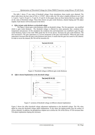
III. VAROATION FACTOR
There are three factors that influence the threshold voltage values (6). The purpose of this variation
factor that more dominant in determine Vth value. The variations values as follow:
Gate oxide thickness
i. Variation 1 – 0.0020um
ii. Variation 2 – 0.0025um
iii. Variation 3 – 0.0060um
Channel Implantation
i. Variation 1 – phos (1.0x10¹³ atom cm1)
ii. Variation 2 - phos (3.5x10¹³ atom cm-1)
iii. Variation 3 – phos (7.0x10¹³ atom cm1)
Channel doping
i. Variation 1 – Boron (1.0x10¹⁵
)
ii. Variation 2 – Boron (2.0x10¹⁵
)
iii. Variation 3 – Boron (4.0x10¹⁵
)
For all three factors above, variation 2 is taken from the simulation. Variation 1 is the half of the variation 2
value and variation 3 is double of the variation 2 value.
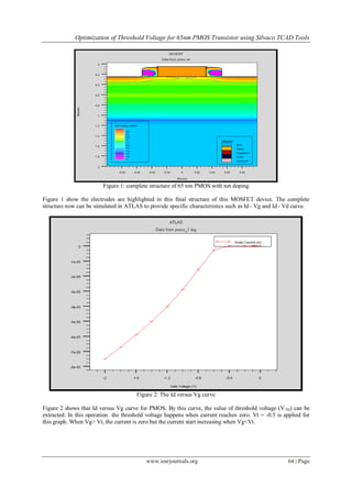
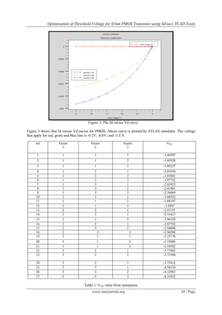
IV. RESULT AND DISCUSION
The results of the fabrication and simulation of 65 nm PMOS can be viewed in the Tony Plot is shown below.
3. Optimization of Threshold Voltage for 65nm PMOS Transistor using Silvaco TCAD Tools
www.iosrjournals.org 64 | Page
Figure 1: complete structure of 65 nm PMOS with net doping
Figure 1 show the electrodes are highlighted in this final structure of this MOSFET device. The complete
structure now can be simulated in ATLAS to provide specific characteristics such as Id - Vg and Id- Vd curve.
Figure 2: The Id versus Vg curve
Figure 2 shows that Id versus Vg curve for PMOS. By this curve, the value of threshold voltage (VTH) can be
extracted. In this operation the threshold voltage happens when current reaches zero. Vt = -0.5 is applied for
this graph. When Vg> Vt, the current is zero but the current start increasing when Vg<Vt.
4. Optimization of Threshold Voltage for 65nm PMOS Transistor using Silvaco TCAD Tools
www.iosrjournals.org 65 | Page
Figure 3: The Id versus Vd curve
Figure 3 shows that Id versus Vd curves for PMOS. Above curve is plotted by ATLAS simulator. The voltage
that apply for red, green and blue line is -0.2V, -0.8V, and -1.2 V.
Table 1: VTH value from simulation
set Factor
1
Factor
2
Factor
3
VTH
1 1 1 1 -1.46993
2 1 1 2 -1.45928
3 1 1 3 -1.45237
4 1 2 1 -2.01034
5 1 2 2 -1.97892
6 1 2 3 -1.97752
7 1 3 1 -2.41923
8 1 3 2 -2.41901
9 1 3 3 -2.56869
10 2 1 1 -1.68352
11 2 1 2 -1.68197
12 2 1 3 -1.6947
13 2 2 1 -2.47151
14 2 2 2 -2.55427
15 2 2 3 -2.46328
16 2 3 1 -2.97793
17 2 3 2 -2.94688
18 2 3 3 -2.94588
19 3 1 1 -2.23176
20 3 1 2 -2.19486
21 3 1 3 -2.18582
22 3 2 1 -3.77602
23 3 2 2 -3.73584
24 3 2 3 -3.73412
25 3 3 1 -4.34154
26 3 3 2 -4.32963
27 3 3 3 -4.31922
5. Optimization of Threshold Voltage for 65nm PMOS Transistor using Silvaco TCAD Tools
www.iosrjournals.org 66 | Page
The table 1 shows 27 sets value of threshold voltage. From simulations, these results were obtained. The
above table shows the best value of Vth is -2.55427. Above table, the Vth value is slightly different in set 2 and
3, 5 and 6, 7 and 8, 10 and 11, 17 and 18, 23 and 24. In this paper, there are three factors that have major effect
on the value of threshold voltage. These three factors are gate oxide thickness, channel doping and Vth adjust
implant. Each factors will be discussed in the below.
A. Effect of gate oxide thickness on threshold voltage
The figure 4 shows gate oxide thickness effect on threshold voltage. The first parameter was modified
which is gate oxide thickness . The threshold voltage is effected by some parameter like: oxidation time,
temperature and pressure. In this simulation the oxidation time and temperature was modified to gate the gate
oxide thickness Value in line with ITRS guide line for 65 nm device. Increases the gate oxide thickness, Vth
also increases(7). The gate capacitance is a reverse proportion of the gate oxide thickness. When the gate oxide
capacitance increases then the gate oxide thickness goes down. It means that the gate less control to the channel.
In order to invert the channel, the Vth will be increases (8).
Figure 4: Threshold voltage at different gate oxide thickness
B. Effect channel implantation to the threshold voltage
Figure 5: variation of threshold voltage at different channel implantation
Figure 5 shows the effect threshold voltage adjustment implantation to the threshold voltage. The Vth value
adjust by using the threshold voltage adjust implantation. It also alters the doping profile near the surface of
silicon substrate. In addition, the phosphorous implant acts to define the Vth of this device. If Vth increases then
Vth adjust implantation doping also increases.
6. Optimization of Threshold Voltage for 65nm PMOS Transistor using Silvaco TCAD Tools
www.iosrjournals.org 67 | Page
C. Effect channel doping to the threshold voltage
Figure 6: Threshold voltage at different channel doping
The figure 6 shows the channel doping increases then the threshold voltage increases, the Fermi potential
increases and the channel depletion charge also increasing, it takes more effort to deplete the whole channel.
Due to that region the Vth increases when the channel doping increases (8).
V. CONCLUSION
There are three factors that effect threshold voltage which is channel doping, gate oxide thickness and
channel implantation. VTH value of 2.55427 is achieved from this simulation. For 65 nm PMOS, the value is in
line with international technology roadmap for semiconductor (ITRS) guideline. Due to punch through effect,
the Id – Vd curve is not saturate.
ACKNOWLEDGEMENTS
I would like to express our sincere thanks to our guides Er. Anil Kumar, Department of Electronics
and Communication Engineering, SSET,SHIATS India, who have been the constant source of motivation for the
successful completion of this work.
I am thankful to Prof. A.K. Jaiswal, Department of Electronics and Communication Engineering,
SSET, SHIATS India, for his devoted encouragement towards the completion of this report. I am also grateful to
Anjani Kumar, Department of Electronics and Communication Engineering, SSET, SHIATS India, for his
support.
I am thankful to our parents and siblings for their emotional support and constant encouragement which
helped us strive and move forward.
REFERENCES
[1] Transistor matching in analog in CMOS applications, IEEE 1998, 34.1.1 - 34.1.4.
[2] Optimization of device performance using semiconductor tcad tools. Silvaco International, Product Description, Silvaco
International. www.silvaco.com/content/kbase/UMichigan_TCAD.pdf
[3] Statistical optimization for process parameters to reduce variability of 32 nm PMOS transistor threshold voltage, International
journal of the physics science vol 6(10), pp. 2372 – 2379, 18 may, 2011
[4] Chapter 3. CMOS Processing Technology, RUNG-Bin Lin,3.1- 3.45.
[5] Taib Ziad Mohamad, Ibrahim ahamd Taib Ziad Mohamad, Ibrahim ahamd, Azami Zaharim, (April 6-8, 2008). Optimum
Solution in FABRICATION 65NM nmos Transistor Using Taguchi Method
[6] Optimization in fabrication 90 nm NMOS transistor using silvaco, Proceeding of 2009 IEEE student conference on research and
development (SCOReD 2009) , 16- 18 Nov’ 09, UPN serdang, Malaysia
[7] 2009. H. Abdullah; J. Jurait; A. Lennie; Z.M. Nopiah; I. Ahmad. Simulation of fabrication process VDMOSFET transistor using
Silvaco software. European Journal
[8] Statistical Optimisation for process parameters to reduce variability of 32nm PMOS transistor threshold voltage, IJPS vol.(6), pp.
2372-2379.
[9] Optimization of process parameter variability in 45 nm PMOS device using Taguchi Method, Journal of Applied Science , ISSN
1812-5654
[10] Gate Engineering on the Analog Performance of DM-DG MOSFETs with High K Dielectrics, International Journal of Advanced
Science and Technology Vol. 25,December, 2010.