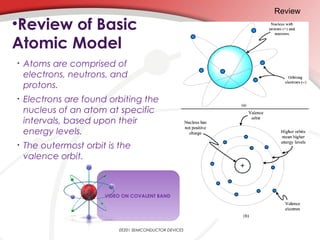
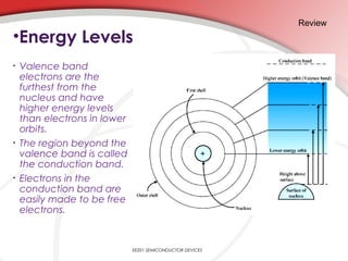
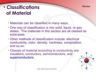
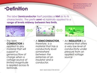
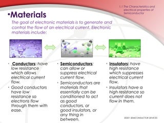
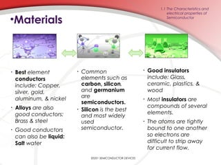
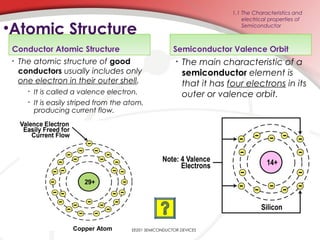
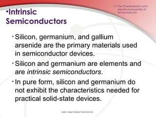
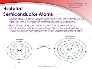
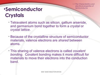
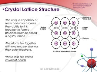
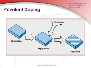
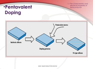
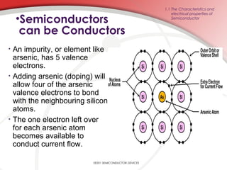
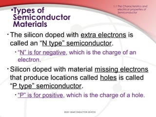
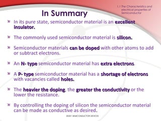
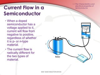
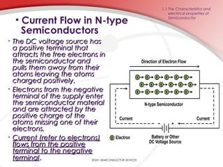
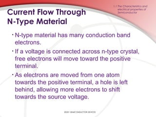
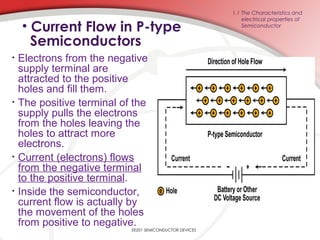
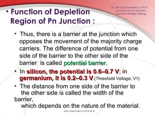
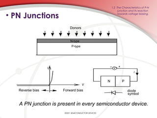
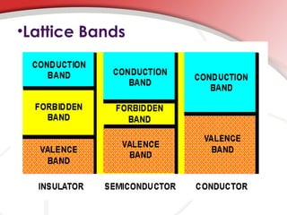
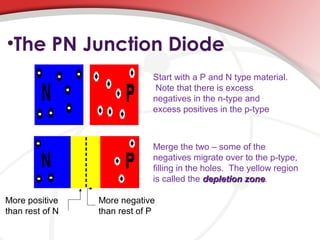
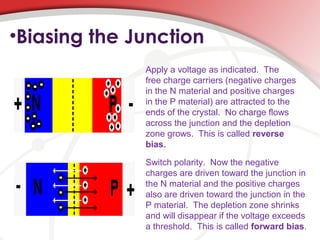
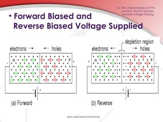
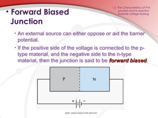
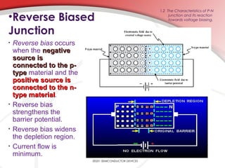
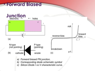
Topic 1: INTRODUCTION TO
SEMICONDUCTOR
EE201
SEMICONDUCTOR DEVICES
Reference’s Book:
“Electronic Devices and
Circuit Theory”
Robert L.Boylestad and Louis Nashelsky
Eight Edition
DEU 2BDEU 2B
LEARNING OUTCOMES
Upon completion of this
Topic 1.0 : Introduction to Semiconductor,
students should be able to:
Understand the Characteristics and electrical
properties of Semiconductors
Identify the effects when a PN junction is supplied with forward
biased voltage and reverse biased voltage
Explain why breakdown occurs when P-N junction is reverse
biased
1.1
Understand the characteristic of P-N junction and
Its reaction towards voltage biasing
1.2
1.2.4
1.2.2
1.2.3
Ilustrate the meaning of Forward biased voltage and
reverse biased voltage supplied across a P-N junction
EE201 SEMICONDUCTOR DEVICES
• A basic understanding of atomic activity
is necessary to understand the operation
and application of semiconductor
devices in electronic circuits.
• Semiconductor devices, such as
transistors and diodes, form the basis of
nearly all modern electronic systems.
• Basic Atomic
Theory
Review
EE201 SEMICONDUCTOR DEVICES
•Review of Basic
Atomic Model
• Atoms are comprised of
electrons, neutrons, and
protons.
• Electrons are found orbiting the
nucleus of an atom at specific
intervals, based upon their
energy levels.
• The outermost orbit is the
valence orbit.
Review
EE201 SEMICONDUCTOR DEVICES
VIDEO ON COVALENT BAND
•Energy Levels
• Valence band
electrons are the
furthest from the
nucleus and have
higher energy levels
than electrons in lower
orbits.
• The region beyond the
valence band is called
the conduction band.
• Electrons in the
conduction band are
easily made to be free
electrons.
Review
EE201 SEMICONDUCTOR DEVICES
• Classifications
of Material
• Materials can be classified in many ways.
• One way of classification is into solid, liquid, or gas
states. The materials in this section are all classed as
solid-state.
• Other methods of classification include: electrical
conductivity, color, density, hardness, composition,
and so on.
• Classes of material according to conductivity are:
insulators, conductors, semiconductors, and
superconductors.
Review
EE201 SEMICONDUCTOR DEVICES
• The term
CONDUCTOR is
applied to any
material that will
support a
generous flow of
charge when a
voltage source of
limited magnitude
is applied across its
terminals.
• A SEMICONDUCTOR,
therefore, is a
material that has a
conductivity level
somewhere
between the
extremes of an
insulator and a
conductor.
• An INSULATOR is a
material that offers
a very low level of
conductivity under
pressure from an
applied voltage
source
•Definition
The label Semiconductor itself provides a hint as to its
characteristic. The prefix semi –is normally applied to a
range of levels midway between two limits.
EE201 SEMICONDUCTOR DEVICES
1.1 The Characteristics and
electrical properties of
Semiconductor
• Conductors: have
low resistance
which allows
electrical current
flow.
• Good conductors
have low
resistance so
electrons flow
through them with
ease.
• Semiconductors:
can allow or
suppress electrical
current flow.
• Semiconductors are
materials that
essentially can be
conditioned to act
as good
conductors, or
good insulators, or
any thing in
between.
• Insulators: have
high resistance
which suppresses
electrical current
flow.
• Insulators have a
high resistance so
current does not
flow in them.
The goal of electronic materials is to generate and
control the flow of an electrical current. Electronic
materials include:
EE201 SEMICONDUCTOR DEVICES
•Materials
1.1 The Characteristics and
electrical properties of
Semiconductor
• Best element
conductors
include: Copper,
silver, gold,
aluminum, & nickel
• Alloys are also
good conductors:
Brass & steel
• Good conductors
can also be liquid:
Salt water
• Common
elements such as
carbon, silicon,
and germanium
are
semiconductors.
• Silicon is the best
and most widely
used
semiconductor.
• Good insulators
include: Glass,
ceramic, plastics, &
wood
• Most insulators are
compounds of several
elements.
• The atoms are tightly
bound to one another
so electrons are
difficult to strip away
for current flow.
EE201 SEMICONDUCTOR DEVICES
•Materials
1.1 The Characteristics and
electrical properties of
Semiconductor
Copper Atom
Conductor Atomic Structure
• The atomic structure of good
conductors usually includes only
one electron in their outer shell.
• It is called a valence electron.
• It is easily striped from the atom,
producing current flow.
• The main characteristic of a
semiconductor element is
that it has four electrons in its
outer or valence orbit.
Semiconductor Valence Orbit
•Atomic Structure
EE201 SEMICONDUCTOR DEVICES
1.1 The Characteristics and
electrical properties of
Semiconductor
•Intrinsic
Semiconductors
• Silicon, germanium, and gallium
arsenide are the primary materials used
in semiconductor devices.
• Silicon and germanium are elements and
are intrinsic semiconductors.
• In pure form, silicon and germanium do
not exhibit the characteristics needed for
practical solid-state devices.
1.1 The Characteristics and
electrical properties of
Semiconductor
EE201 SEMICONDUCTOR DEVICES
•Isolated
Semiconductor Atoms
• Silicon and Germanium are electrically neutral; that is, each
has the same number of orbiting electrons as protons.
• Both silicon and germanium have four valence band
electrons, and so they are referred to as tetravalent atoms.
This is an important characteristic of semiconductor atoms.
1.1 The Characteristics and
electrical properties of
Semiconductor
EE201 SEMICONDUCTOR DEVICES
•Semiconductor
Crystals
• Tetravalent atoms such as silicon, gallium arsenide,
and germanium bond together to form a crystal or
crystal lattice.
• Because of the crystalline structure of semiconductor
materials, valence electrons are shared between
atoms.
• This sharing of valence electrons is called covalent
bonding. Covalent bonding makes it more difficult for
materials to move their electrons into the conduction
band.
1.1 The Characteristics and
electrical properties of
Semiconductor
EE201 SEMICONDUCTOR DEVICES
•The unique capability of
semiconductor atoms is
their ability to link
together to form a
physical structure called
a crystal lattice
•The atoms link together
with one another sharing
their outer electrons.
•These links are called
covalent bonds
•Crystal Lattice Structure
EE201 SEMICONDUCTOR DEVICES
1.1 The Characteristics and
electrical properties of
Semiconductor
• If the material is pure semiconductor material like silicon,
the crystal lattice structure forms an excellent insulator
since all the atoms are bound to one another and are not
free for current flow.
• Good insulating semiconductor material is referred to as
intrinsic.
• Since the outer valence electrons of each atom are tightly
bound together with one another, the electrons
are difficult to get free for current flow.
• Silicon in this form is a great insulator.
• Semiconductor material is often used as an insulator.
•Semiconductors can
be Insulators
1.1 The Characteristics and
electrical properties of
Semiconductor
EE201 SEMICONDUCTOR DEVICES
Impurities are added to intrinsic
semiconductor materials to improve the
electrical properties of the material.
Impurities” are different elements.
This process is called doping and the
resulting material is called extrinsic
semiconductor.
There are two major classifications of
doping materials.
i. Trivalent - aluminum, gallium,boron
ii. Pentavalent - antimony, arsenic,
phosphorous
1.1 The Characteristics and
electrical properties of
SemiconductorSemiconductor
Doping
•Trivalent Doping
• SiliconSilicon is the most widely used semiconductor
material.
• By adding a trivalenttrivalent material to the crystal
structure, holesholes are introduced and provide a
mechanism for conduction.
• Because trivalent materials can accept an
additional electron, they are called acceptor
atoms.
• A silicon crystal doped with trivalent material is
called p-type material.
1.1 The Characteristics and
electrical properties of
Semiconductor
EE201 SEMICONDUCTOR DEVICES
•Trivalent Doping
1.1 The Characteristics and
electrical properties of
Semiconductor
EE201 SEMICONDUCTOR DEVICES
•Pentavalent
Doping
• Doping silicon with pentavalentpentavalent material results
in extra electronsextra electrons being available, improving
the conduction characteristics.
• Pentavalent materials donate electrons, and
therefore are called donor atoms.
• Once a silicon crystal has been doped with
pentavalent materials, it is called n-type
semiconductor material.
1.1 The Characteristics and
electrical properties of
Semiconductor
EE201 SEMICONDUCTOR DEVICES
•Pentavalent
Doping
EE201 SEMICONDUCTOR DEVICES
1.1 The Characteristics and
electrical properties of
Semiconductor
EE201 SEMICONDUCTOR DEVICES
•Semiconductors
can be Conductors
• An impurity, or element like
arsenic, has 5 valence
electrons.
• Adding arsenic (doping) will
allow four of the arsenic
valence electrons to bond
with the neighbouring silicon
atoms.
• The one electron left over
for each arsenic atom
becomes available to
conduct current flow.
1.1 The Characteristics and
electrical properties of
Semiconductor
•Types of
Semiconductor
Materials
EE201 SEMICONDUCTOR DEVICES
• The silicon doped with extra electrons is
called an “N type” semiconductor.
• “N” is for negative, which is the charge of an
electron.
• Silicon doped with material missing electrons
that produce locations called holes is called
“P type” semiconductor.
• “P” is for positive, which is the charge of a hole.
1.1 The Characteristics and
electrical properties of
Semiconductor
•Energy Levels
1.1 The Characteristics and
electrical properties of
Semiconductor
In Summary
In its pure state, semiconductor material is an excellentexcellent
insulator.insulator.
The commonly used semiconductor material is silicon.silicon.
Semiconductor materials can be dopedcan be doped with other atoms to add
or subtract electrons.
An N- typeN- type semiconductor material has extra electronsextra electrons.
A P- typeP- type semiconductor material has a shortage of electronsshortage of electrons
with vacancies called holes.holes.
The heavier the dopingheavier the doping, the greater the conductivitygreater the conductivity or the
lower the resistance.
By controlling the doping of silicon the semiconductor material
can be made as conductive as desired.
EE201 SEMICONDUCTOR DEVICES
1.1 The Characteristics and
electrical properties of
Semiconductor
EE201 SEMICONDUCTOR DEVICES
Current Flow in a
Semiconductor
• When a doped
semiconductor has a
voltage applied to it,
current will flow from
negative to positive,
regardless of whether
it is p- or n-type
material.
• The current flow is
radically different for
the two types of
material.
1.1 The Characteristics and
electrical properties of
Semiconductor
• Current Flow in N-type
Semiconductors
EE201 SEMICONDUCTOR DEVICES
• The DC voltage source hasThe DC voltage source has
a positive terminal thata positive terminal that
attracts the free electrons inattracts the free electrons in
the semiconductor andthe semiconductor and
pulls them away from theirpulls them away from their
atoms leaving the atomsatoms leaving the atoms
charged positively.charged positively.
• Electrons from the negativeElectrons from the negative
terminal of the supply enterterminal of the supply enter
the semiconductor materialthe semiconductor material
and are attracted by theand are attracted by the
positive charge of thepositive charge of the
atoms missing one of theiratoms missing one of their
electrons.electrons.
• Current (refer to electrons)Current (refer to electrons)
flows from the positiveflows from the positive
terminal to the negativeterminal to the negative
terminalterminal..
1.1 The Characteristics and
electrical properties of
Semiconductor
EE201 SEMICONDUCTOR DEVICES
Current Flow Through
N-Type Material
• N-type material has many conduction band
electrons.
• If a voltage is connected across n-type crystal,
free electrons will move toward the positive
terminal.
• As electrons are moved from one atom
towards the positive terminal, a hole is left
behind, allowing more electrons to shift
towards the source voltage.
1.1 The Characteristics and
electrical properties of
Semiconductor
• Current Flow in P-type
Semiconductors
EE201 SEMICONDUCTOR DEVICES
• Electrons from the negative
supply terminal are
attracted to the positive
holes and fill them.
• The positive terminal of the
supply pulls the electrons
from the holes leaving the
holes to attract more
electrons.
• Current (electrons) flows
from the negative terminal
to the positive terminal.
• Inside the semiconductor,
current flow is actually by
the movement of the holes
from positive to negative.
1.1 The Characteristics and
electrical properties of
Semiconductor
EE201 SEMICONDUCTOR DEVICES
Current Flow Through
P-Type Material
Current flow in p-type material causes the
shift of “holes” towards the negative terminal
because of the shifting of the covalent
electrons.
Hole flow moves from positive to negative in
a p-type semiconductor material.
Actual current flow is still electron current flow
from negative to positive.
1.1 The Characteristics and
electrical properties of
Semiconductor
EE201 SEMICONDUCTOR DEVICES
Electron versus
Hole Flow
• Electron flow in p-typeElectron flow in p-type
material occurs in thematerial occurs in the
valence bandvalence band;; electron
movement in n-type
material occurs in the
conduction band
• Electrons are the majority
carriers in n-type
material; they are holesthey are holes
in p-type material.in p-type material.
1.1 The Characteristics and
electrical properties of
Semiconductor
EE201 SEMICONDUCTOR DEVICES
1.2 The Characteristics of P-N
junction and its reaction
towards voltage biasing.
Semiconductor
Junctions
• When p-type
material meets
n-type material
within a single
silicon crystal, a PN
junction is formed.
EE201 SEMICONDUCTOR DEVICES
1.2 The Characteristics of P-N
junction and its reaction
towards voltage biasing.
Unbiased Junction
• The pn junction is formed in the process of
creating the semiconductor device.
• Before carrier migration, there are equal
numbers of holes and electrons on either side
of the junction.
• Because of random thermal energy, some
electrons will pass across the pn junction
mating with holes on the other side. This is
called recombinationrecombination.
•Formation Of Depletion
Region/Layer
EE201 SEMICONDUCTOR DEVICES
1.2 The Characteristics of P-N
junction and its reaction
towards voltage biasing.
• As soon as the junction is formed, free electrons
and holes cross through the junction by the
process of diffusion.
• During this process , the electrons crossing the
junction from N- region into P-region , recombine
with holes in the P-region very close to the
junction.
• Similarly holes crossing the junction from the P-
region into the N-region, recombine with electrons
in the N-region very close to the junction.
• Depletion Region/Layer
EE201 SEMICONDUCTOR DEVICES
1.2 The Characteristics of P-N
junction and its reaction
towards voltage biasing.
• After a time, the region will be depleted of
charge carriers because of the migration of
electrons and holes.
• This leaves an area known as the
depletion region/ layerdepletion region/ layer in the pn junction,
which does not have any mobile charge
very close to the junction.
EE201 SEMICONDUCTOR DEVICES
1.2 The Characteristics of P-N
junction and its reaction
towards voltage biasing.
In this region, on the left side of
the junction, the acceptoracceptor
atoms become negative ionsatoms become negative ions
(an atom gains electrons,(an atom gains electrons,
number of electrons exceednumber of electrons exceed
from the number of protonfrom the number of proton
and hence an atom getsand hence an atom gets
negatively charged)negatively charged)
and on the right side of the
junction, the donor atomsdonor atoms
become positive ionsbecome positive ions (an(an
atom looses electrons theatom looses electrons the
total number of protonstotal number of protons
become more than thebecome more than the
number of electrons and thenumber of electrons and the
atom becomes positivelyatom becomes positively
charged)charged)
• Depletion Region/Layer
• Function of Depletion
Region of Pn Junction :
EE201 SEMICONDUCTOR DEVICES
1.2 The Characteristics of P-N
junction and its reaction
towards voltage biasing.
• An electric field is set up, between the donor and
acceptor ions in the depletion layer of the pn
junction .
• The potential at the N-side is higher than the
potential at P-side.Therefore electrons in the N-
side are prevented to go to the lower potential of
P-side.
• Similarly, holes in the P-side find themselves at a
lower potential and are prevented to cross to the N-
side.
• Function of Depletion
Region of Pn Junction :
EE201 SEMICONDUCTOR DEVICES
1.2 The Characteristics of P-N
junction and its reaction
towards voltage biasing.
• Thus, there is a barrier at the junction which
opposes the movement of the majority charge
carriers. The difference of potential from one
side of the barrier to the other side of the
barrier is called potential barrier.potential barrier.
• In silicon, the potential is 0.6–0.7 Vsilicon, the potential is 0.6–0.7 V; in
germanium, it is 0.2–0.3 Vgermanium, it is 0.2–0.3 V.(Threshold Voltage, VT)
• The distance from one side of the barrier to
the other side is called the width of the
barrier,
which depends on the nature of the material.
A PN junction is present in every semiconductor device.
N-type
P-type
Donors
V
I
Reverse bias Forward bias
N P
V
I
diode
symbol
– +
• PN Junctions
1.2 The Characteristics of P-N
junction and its reaction
towards voltage biasing.
EE201 SEMICONDUCTOR DEVICES
•Lattice Bands
•Conduction
• In order for an electron to become free and
participate in current flow, it must gain enough
energy to jump over the forbidden band.
• For semiconductors at room temperature, there is
not enough energy to conduct.
• As temperature increases more electrons have the
energy to jump the forbidden band
• Resistivity decreasesResistivity decreases
• This is the opposite behavior of conductorsThis is the opposite behavior of conductors
•The PN Junction Diode
Start with a P and N type material.
Note that there is excess
negatives in the n-type and
excess positives in the p-type
Merge the two – some of the
negatives migrate over to the p-type,
filling in the holes. The yellow region
is called the depletion zonedepletion zone.
More positive
than rest of N
More negative
than rest of P
•Biasing the Junction
Apply a voltage as indicated. The
free charge carriers (negative charges
in the N material and positive charges
in the P material) are attracted to the
ends of the crystal. No charge flows
across the junction and the depletion
zone grows. This is called reverse
bias.
Switch polarity. Now the negative
charges are driven toward the junction in
the N material and the positive charges
also are driven toward the junction in the
P material. The depletion zone shrinks
and will disappear if the voltage exceeds
a threshold. This is called forward bias.
• Forward Biased and
Reverse Biased Voltage Supplied
EE201 SEMICONDUCTOR DEVICES
1.2 The Characteristics of P-N
junction and its reaction
towards voltage biasing.
EE201 SEMICONDUCTOR DEVICES
1.2 The Characteristics of P-N
junction and its reaction
towards voltage biasing.• Forward Biased
Junction
• An external source can either oppose or aid the barrier
potential.
• If the positive side of the voltage is connected to the p-
type material, and the negative side to the n-type
material, then the junction is said to be forward biasedforward biased.
EE201 SEMICONDUCTOR DEVICES
1.2 The Characteristics of P-N
junction and its reaction
towards voltage biasing.
• Forward Biased
Junction
• In a forward biased junction, the
following conditions exist:
• Forward bias overcomes barrier potential.
• Forward bias narrows the depletion region.
• There is maximum current flow with
forward bias.
EE201 SEMICONDUCTOR DEVICES
1.2 The Characteristics of P-N
junction and its reaction
towards voltage biasing.•Reverse Biased
Junction
• Reverse bias occurs
when the negativenegative
source issource is
connected to the p-connected to the p-
typetype material and the
positive source ispositive source is
connected to the n-connected to the n-
type materialtype material.
• Reverse bias
strengthens the
barrier potential.
• Reverse bias widens
the depletion region.
• Current flow is
minimum.
a) Forward biased PN junction,
b) Corresponding diode schematic symbol
c) Silicon Diode I vs V characteristic curve.
• Forward Biased
Junction
• Characteristics of
Reverse Bias PN Junction:
EE201 SEMICONDUCTOR DEVICES
1.2 The Characteristics of P-N
junction and its reaction
towards voltage biasing.
• From the characteristic curve, it can be concluded that,
as voltage is increased from zero, reverse current (Ir)
(in the order of microamperes) increases and reaches
the maximum value at a small value of reverse voltage
(Vr).
• When the voltage is further increased, the current is
almost independent of the reverse voltage up to a certain
critical value.
• This reverse current is known as the reverse saturation
current or leakage current.
• This current is due to the minority charge carriers, which
depends on junction temperature.
EE201 SEMICONDUCTOR DEVICES
1.2 The Characteristics of P-N
junction and its reaction
towards voltage biasing.
•Reverse Biased
Junction
• A reversed biased junction has zero current flow
(ideally).
• Reverse current is temperature dependent.
• If reverse biased is increased enough, the reverse
current increases dramatically.
• This breakdown is called junction breakdownjunction breakdown. The
voltage required to reach this point is the reversereverse
breakdown voltagebreakdown voltage..
• As the breakdown occurs, avalancheavalanche may occur and
destroy the device if uncontrolled.
EE201 SEMICONDUCTOR DEVICES
1.2 The Characteristics of P-N
junction and its reaction
towards voltage biasing.
•Review…..
• Breakdowns in Reverse
Biased
1.2 The Characteristics of P-N
junction and its reaction
towards voltage biasing.
• There are two mechanisms by which
breakdown can occur at a reverse biased P-N
junction : avalanche breakdown and
Zener/Tunneling breakdown.
Diode I vs V characteristic curve.)
EE201 SEMICONDUCTOR DEVICES
Junction Breakdown
A Zener diode is designed to operate in the breakdown
mode.
V
I
V
B
, breakdown
Forward Current
Small leakage
Current
voltage
1.2 The Characteristics of P-N
junction and its reaction
towards voltage biasing.
EE201 SEMICONDUCTOR DEVICES
Thanks…

Topic 1 ee201[1]

  • 1.
    Topic 1: INTRODUCTIONTO SEMICONDUCTOR EE201 SEMICONDUCTOR DEVICES Reference’s Book: “Electronic Devices and Circuit Theory” Robert L.Boylestad and Louis Nashelsky Eight Edition DEU 2BDEU 2B
  • 2.
    LEARNING OUTCOMES Upon completionof this Topic 1.0 : Introduction to Semiconductor, students should be able to: Understand the Characteristics and electrical properties of Semiconductors Identify the effects when a PN junction is supplied with forward biased voltage and reverse biased voltage Explain why breakdown occurs when P-N junction is reverse biased 1.1 Understand the characteristic of P-N junction and Its reaction towards voltage biasing 1.2 1.2.4 1.2.2 1.2.3 Ilustrate the meaning of Forward biased voltage and reverse biased voltage supplied across a P-N junction EE201 SEMICONDUCTOR DEVICES
  • 3.
    • A basicunderstanding of atomic activity is necessary to understand the operation and application of semiconductor devices in electronic circuits. • Semiconductor devices, such as transistors and diodes, form the basis of nearly all modern electronic systems. • Basic Atomic Theory Review EE201 SEMICONDUCTOR DEVICES
  • 4.
    •Review of Basic AtomicModel • Atoms are comprised of electrons, neutrons, and protons. • Electrons are found orbiting the nucleus of an atom at specific intervals, based upon their energy levels. • The outermost orbit is the valence orbit. Review EE201 SEMICONDUCTOR DEVICES VIDEO ON COVALENT BAND
  • 5.
    •Energy Levels • Valenceband electrons are the furthest from the nucleus and have higher energy levels than electrons in lower orbits. • The region beyond the valence band is called the conduction band. • Electrons in the conduction band are easily made to be free electrons. Review EE201 SEMICONDUCTOR DEVICES
  • 6.
    • Classifications of Material •Materials can be classified in many ways. • One way of classification is into solid, liquid, or gas states. The materials in this section are all classed as solid-state. • Other methods of classification include: electrical conductivity, color, density, hardness, composition, and so on. • Classes of material according to conductivity are: insulators, conductors, semiconductors, and superconductors. Review EE201 SEMICONDUCTOR DEVICES
  • 7.
    • The term CONDUCTORis applied to any material that will support a generous flow of charge when a voltage source of limited magnitude is applied across its terminals. • A SEMICONDUCTOR, therefore, is a material that has a conductivity level somewhere between the extremes of an insulator and a conductor. • An INSULATOR is a material that offers a very low level of conductivity under pressure from an applied voltage source •Definition The label Semiconductor itself provides a hint as to its characteristic. The prefix semi –is normally applied to a range of levels midway between two limits. EE201 SEMICONDUCTOR DEVICES 1.1 The Characteristics and electrical properties of Semiconductor
  • 8.
    • Conductors: have lowresistance which allows electrical current flow. • Good conductors have low resistance so electrons flow through them with ease. • Semiconductors: can allow or suppress electrical current flow. • Semiconductors are materials that essentially can be conditioned to act as good conductors, or good insulators, or any thing in between. • Insulators: have high resistance which suppresses electrical current flow. • Insulators have a high resistance so current does not flow in them. The goal of electronic materials is to generate and control the flow of an electrical current. Electronic materials include: EE201 SEMICONDUCTOR DEVICES •Materials 1.1 The Characteristics and electrical properties of Semiconductor
  • 9.
    • Best element conductors include:Copper, silver, gold, aluminum, & nickel • Alloys are also good conductors: Brass & steel • Good conductors can also be liquid: Salt water • Common elements such as carbon, silicon, and germanium are semiconductors. • Silicon is the best and most widely used semiconductor. • Good insulators include: Glass, ceramic, plastics, & wood • Most insulators are compounds of several elements. • The atoms are tightly bound to one another so electrons are difficult to strip away for current flow. EE201 SEMICONDUCTOR DEVICES •Materials 1.1 The Characteristics and electrical properties of Semiconductor
  • 10.
    Copper Atom Conductor AtomicStructure • The atomic structure of good conductors usually includes only one electron in their outer shell. • It is called a valence electron. • It is easily striped from the atom, producing current flow. • The main characteristic of a semiconductor element is that it has four electrons in its outer or valence orbit. Semiconductor Valence Orbit •Atomic Structure EE201 SEMICONDUCTOR DEVICES 1.1 The Characteristics and electrical properties of Semiconductor
  • 11.
    •Intrinsic Semiconductors • Silicon, germanium,and gallium arsenide are the primary materials used in semiconductor devices. • Silicon and germanium are elements and are intrinsic semiconductors. • In pure form, silicon and germanium do not exhibit the characteristics needed for practical solid-state devices. 1.1 The Characteristics and electrical properties of Semiconductor EE201 SEMICONDUCTOR DEVICES
  • 12.
    •Isolated Semiconductor Atoms • Siliconand Germanium are electrically neutral; that is, each has the same number of orbiting electrons as protons. • Both silicon and germanium have four valence band electrons, and so they are referred to as tetravalent atoms. This is an important characteristic of semiconductor atoms. 1.1 The Characteristics and electrical properties of Semiconductor EE201 SEMICONDUCTOR DEVICES
  • 13.
    •Semiconductor Crystals • Tetravalent atomssuch as silicon, gallium arsenide, and germanium bond together to form a crystal or crystal lattice. • Because of the crystalline structure of semiconductor materials, valence electrons are shared between atoms. • This sharing of valence electrons is called covalent bonding. Covalent bonding makes it more difficult for materials to move their electrons into the conduction band. 1.1 The Characteristics and electrical properties of Semiconductor EE201 SEMICONDUCTOR DEVICES
  • 14.
    •The unique capabilityof semiconductor atoms is their ability to link together to form a physical structure called a crystal lattice •The atoms link together with one another sharing their outer electrons. •These links are called covalent bonds •Crystal Lattice Structure EE201 SEMICONDUCTOR DEVICES 1.1 The Characteristics and electrical properties of Semiconductor
  • 15.
    • If thematerial is pure semiconductor material like silicon, the crystal lattice structure forms an excellent insulator since all the atoms are bound to one another and are not free for current flow. • Good insulating semiconductor material is referred to as intrinsic. • Since the outer valence electrons of each atom are tightly bound together with one another, the electrons are difficult to get free for current flow. • Silicon in this form is a great insulator. • Semiconductor material is often used as an insulator. •Semiconductors can be Insulators 1.1 The Characteristics and electrical properties of Semiconductor EE201 SEMICONDUCTOR DEVICES
  • 16.
    EE201 SEMICONDUCTOR DEVICES Impuritiesare added to intrinsic semiconductor materials to improve the electrical properties of the material. Impurities” are different elements. This process is called doping and the resulting material is called extrinsic semiconductor. There are two major classifications of doping materials. i. Trivalent - aluminum, gallium,boron ii. Pentavalent - antimony, arsenic, phosphorous 1.1 The Characteristics and electrical properties of SemiconductorSemiconductor Doping
  • 17.
    •Trivalent Doping • SiliconSiliconis the most widely used semiconductor material. • By adding a trivalenttrivalent material to the crystal structure, holesholes are introduced and provide a mechanism for conduction. • Because trivalent materials can accept an additional electron, they are called acceptor atoms. • A silicon crystal doped with trivalent material is called p-type material. 1.1 The Characteristics and electrical properties of Semiconductor EE201 SEMICONDUCTOR DEVICES
  • 18.
    •Trivalent Doping 1.1 TheCharacteristics and electrical properties of Semiconductor EE201 SEMICONDUCTOR DEVICES
  • 19.
    •Pentavalent Doping • Doping siliconwith pentavalentpentavalent material results in extra electronsextra electrons being available, improving the conduction characteristics. • Pentavalent materials donate electrons, and therefore are called donor atoms. • Once a silicon crystal has been doped with pentavalent materials, it is called n-type semiconductor material. 1.1 The Characteristics and electrical properties of Semiconductor EE201 SEMICONDUCTOR DEVICES
  • 20.
    •Pentavalent Doping EE201 SEMICONDUCTOR DEVICES 1.1The Characteristics and electrical properties of Semiconductor
  • 21.
    EE201 SEMICONDUCTOR DEVICES •Semiconductors canbe Conductors • An impurity, or element like arsenic, has 5 valence electrons. • Adding arsenic (doping) will allow four of the arsenic valence electrons to bond with the neighbouring silicon atoms. • The one electron left over for each arsenic atom becomes available to conduct current flow. 1.1 The Characteristics and electrical properties of Semiconductor
  • 22.
    •Types of Semiconductor Materials EE201 SEMICONDUCTORDEVICES • The silicon doped with extra electrons is called an “N type” semiconductor. • “N” is for negative, which is the charge of an electron. • Silicon doped with material missing electrons that produce locations called holes is called “P type” semiconductor. • “P” is for positive, which is the charge of a hole. 1.1 The Characteristics and electrical properties of Semiconductor
  • 23.
    •Energy Levels 1.1 TheCharacteristics and electrical properties of Semiconductor
  • 24.
    In Summary In itspure state, semiconductor material is an excellentexcellent insulator.insulator. The commonly used semiconductor material is silicon.silicon. Semiconductor materials can be dopedcan be doped with other atoms to add or subtract electrons. An N- typeN- type semiconductor material has extra electronsextra electrons. A P- typeP- type semiconductor material has a shortage of electronsshortage of electrons with vacancies called holes.holes. The heavier the dopingheavier the doping, the greater the conductivitygreater the conductivity or the lower the resistance. By controlling the doping of silicon the semiconductor material can be made as conductive as desired. EE201 SEMICONDUCTOR DEVICES 1.1 The Characteristics and electrical properties of Semiconductor
  • 25.
    EE201 SEMICONDUCTOR DEVICES CurrentFlow in a Semiconductor • When a doped semiconductor has a voltage applied to it, current will flow from negative to positive, regardless of whether it is p- or n-type material. • The current flow is radically different for the two types of material. 1.1 The Characteristics and electrical properties of Semiconductor
  • 26.
    • Current Flowin N-type Semiconductors EE201 SEMICONDUCTOR DEVICES • The DC voltage source hasThe DC voltage source has a positive terminal thata positive terminal that attracts the free electrons inattracts the free electrons in the semiconductor andthe semiconductor and pulls them away from theirpulls them away from their atoms leaving the atomsatoms leaving the atoms charged positively.charged positively. • Electrons from the negativeElectrons from the negative terminal of the supply enterterminal of the supply enter the semiconductor materialthe semiconductor material and are attracted by theand are attracted by the positive charge of thepositive charge of the atoms missing one of theiratoms missing one of their electrons.electrons. • Current (refer to electrons)Current (refer to electrons) flows from the positiveflows from the positive terminal to the negativeterminal to the negative terminalterminal.. 1.1 The Characteristics and electrical properties of Semiconductor
  • 27.
    EE201 SEMICONDUCTOR DEVICES CurrentFlow Through N-Type Material • N-type material has many conduction band electrons. • If a voltage is connected across n-type crystal, free electrons will move toward the positive terminal. • As electrons are moved from one atom towards the positive terminal, a hole is left behind, allowing more electrons to shift towards the source voltage. 1.1 The Characteristics and electrical properties of Semiconductor
  • 28.
    • Current Flowin P-type Semiconductors EE201 SEMICONDUCTOR DEVICES • Electrons from the negative supply terminal are attracted to the positive holes and fill them. • The positive terminal of the supply pulls the electrons from the holes leaving the holes to attract more electrons. • Current (electrons) flows from the negative terminal to the positive terminal. • Inside the semiconductor, current flow is actually by the movement of the holes from positive to negative. 1.1 The Characteristics and electrical properties of Semiconductor
  • 29.
    EE201 SEMICONDUCTOR DEVICES CurrentFlow Through P-Type Material Current flow in p-type material causes the shift of “holes” towards the negative terminal because of the shifting of the covalent electrons. Hole flow moves from positive to negative in a p-type semiconductor material. Actual current flow is still electron current flow from negative to positive. 1.1 The Characteristics and electrical properties of Semiconductor
  • 30.
    EE201 SEMICONDUCTOR DEVICES Electronversus Hole Flow • Electron flow in p-typeElectron flow in p-type material occurs in thematerial occurs in the valence bandvalence band;; electron movement in n-type material occurs in the conduction band • Electrons are the majority carriers in n-type material; they are holesthey are holes in p-type material.in p-type material. 1.1 The Characteristics and electrical properties of Semiconductor
  • 31.
    EE201 SEMICONDUCTOR DEVICES 1.2The Characteristics of P-N junction and its reaction towards voltage biasing. Semiconductor Junctions • When p-type material meets n-type material within a single silicon crystal, a PN junction is formed.
  • 32.
    EE201 SEMICONDUCTOR DEVICES 1.2The Characteristics of P-N junction and its reaction towards voltage biasing. Unbiased Junction • The pn junction is formed in the process of creating the semiconductor device. • Before carrier migration, there are equal numbers of holes and electrons on either side of the junction. • Because of random thermal energy, some electrons will pass across the pn junction mating with holes on the other side. This is called recombinationrecombination.
  • 33.
    •Formation Of Depletion Region/Layer EE201SEMICONDUCTOR DEVICES 1.2 The Characteristics of P-N junction and its reaction towards voltage biasing. • As soon as the junction is formed, free electrons and holes cross through the junction by the process of diffusion. • During this process , the electrons crossing the junction from N- region into P-region , recombine with holes in the P-region very close to the junction. • Similarly holes crossing the junction from the P- region into the N-region, recombine with electrons in the N-region very close to the junction.
  • 34.
    • Depletion Region/Layer EE201SEMICONDUCTOR DEVICES 1.2 The Characteristics of P-N junction and its reaction towards voltage biasing. • After a time, the region will be depleted of charge carriers because of the migration of electrons and holes. • This leaves an area known as the depletion region/ layerdepletion region/ layer in the pn junction, which does not have any mobile charge very close to the junction.
  • 35.
    EE201 SEMICONDUCTOR DEVICES 1.2The Characteristics of P-N junction and its reaction towards voltage biasing. In this region, on the left side of the junction, the acceptoracceptor atoms become negative ionsatoms become negative ions (an atom gains electrons,(an atom gains electrons, number of electrons exceednumber of electrons exceed from the number of protonfrom the number of proton and hence an atom getsand hence an atom gets negatively charged)negatively charged) and on the right side of the junction, the donor atomsdonor atoms become positive ionsbecome positive ions (an(an atom looses electrons theatom looses electrons the total number of protonstotal number of protons become more than thebecome more than the number of electrons and thenumber of electrons and the atom becomes positivelyatom becomes positively charged)charged) • Depletion Region/Layer
  • 36.
    • Function ofDepletion Region of Pn Junction : EE201 SEMICONDUCTOR DEVICES 1.2 The Characteristics of P-N junction and its reaction towards voltage biasing. • An electric field is set up, between the donor and acceptor ions in the depletion layer of the pn junction . • The potential at the N-side is higher than the potential at P-side.Therefore electrons in the N- side are prevented to go to the lower potential of P-side. • Similarly, holes in the P-side find themselves at a lower potential and are prevented to cross to the N- side.
  • 37.
    • Function ofDepletion Region of Pn Junction : EE201 SEMICONDUCTOR DEVICES 1.2 The Characteristics of P-N junction and its reaction towards voltage biasing. • Thus, there is a barrier at the junction which opposes the movement of the majority charge carriers. The difference of potential from one side of the barrier to the other side of the barrier is called potential barrier.potential barrier. • In silicon, the potential is 0.6–0.7 Vsilicon, the potential is 0.6–0.7 V; in germanium, it is 0.2–0.3 Vgermanium, it is 0.2–0.3 V.(Threshold Voltage, VT) • The distance from one side of the barrier to the other side is called the width of the barrier, which depends on the nature of the material.
  • 38.
    A PN junctionis present in every semiconductor device. N-type P-type Donors V I Reverse bias Forward bias N P V I diode symbol – + • PN Junctions 1.2 The Characteristics of P-N junction and its reaction towards voltage biasing. EE201 SEMICONDUCTOR DEVICES
  • 39.
  • 40.
    •Conduction • In orderfor an electron to become free and participate in current flow, it must gain enough energy to jump over the forbidden band. • For semiconductors at room temperature, there is not enough energy to conduct. • As temperature increases more electrons have the energy to jump the forbidden band • Resistivity decreasesResistivity decreases • This is the opposite behavior of conductorsThis is the opposite behavior of conductors
  • 41.
    •The PN JunctionDiode Start with a P and N type material. Note that there is excess negatives in the n-type and excess positives in the p-type Merge the two – some of the negatives migrate over to the p-type, filling in the holes. The yellow region is called the depletion zonedepletion zone. More positive than rest of N More negative than rest of P
  • 42.
    •Biasing the Junction Applya voltage as indicated. The free charge carriers (negative charges in the N material and positive charges in the P material) are attracted to the ends of the crystal. No charge flows across the junction and the depletion zone grows. This is called reverse bias. Switch polarity. Now the negative charges are driven toward the junction in the N material and the positive charges also are driven toward the junction in the P material. The depletion zone shrinks and will disappear if the voltage exceeds a threshold. This is called forward bias.
  • 43.
    • Forward Biasedand Reverse Biased Voltage Supplied EE201 SEMICONDUCTOR DEVICES 1.2 The Characteristics of P-N junction and its reaction towards voltage biasing.
  • 44.
    EE201 SEMICONDUCTOR DEVICES 1.2The Characteristics of P-N junction and its reaction towards voltage biasing.• Forward Biased Junction • An external source can either oppose or aid the barrier potential. • If the positive side of the voltage is connected to the p- type material, and the negative side to the n-type material, then the junction is said to be forward biasedforward biased.
  • 45.
    EE201 SEMICONDUCTOR DEVICES 1.2The Characteristics of P-N junction and its reaction towards voltage biasing. • Forward Biased Junction • In a forward biased junction, the following conditions exist: • Forward bias overcomes barrier potential. • Forward bias narrows the depletion region. • There is maximum current flow with forward bias.
  • 46.
    EE201 SEMICONDUCTOR DEVICES 1.2The Characteristics of P-N junction and its reaction towards voltage biasing.•Reverse Biased Junction • Reverse bias occurs when the negativenegative source issource is connected to the p-connected to the p- typetype material and the positive source ispositive source is connected to the n-connected to the n- type materialtype material. • Reverse bias strengthens the barrier potential. • Reverse bias widens the depletion region. • Current flow is minimum.
  • 47.
    a) Forward biasedPN junction, b) Corresponding diode schematic symbol c) Silicon Diode I vs V characteristic curve. • Forward Biased Junction
  • 48.
    • Characteristics of ReverseBias PN Junction: EE201 SEMICONDUCTOR DEVICES 1.2 The Characteristics of P-N junction and its reaction towards voltage biasing. • From the characteristic curve, it can be concluded that, as voltage is increased from zero, reverse current (Ir) (in the order of microamperes) increases and reaches the maximum value at a small value of reverse voltage (Vr). • When the voltage is further increased, the current is almost independent of the reverse voltage up to a certain critical value. • This reverse current is known as the reverse saturation current or leakage current. • This current is due to the minority charge carriers, which depends on junction temperature.
  • 49.
    EE201 SEMICONDUCTOR DEVICES 1.2The Characteristics of P-N junction and its reaction towards voltage biasing. •Reverse Biased Junction • A reversed biased junction has zero current flow (ideally). • Reverse current is temperature dependent. • If reverse biased is increased enough, the reverse current increases dramatically. • This breakdown is called junction breakdownjunction breakdown. The voltage required to reach this point is the reversereverse breakdown voltagebreakdown voltage.. • As the breakdown occurs, avalancheavalanche may occur and destroy the device if uncontrolled.
  • 50.
    EE201 SEMICONDUCTOR DEVICES 1.2The Characteristics of P-N junction and its reaction towards voltage biasing. •Review…..
  • 51.
    • Breakdowns inReverse Biased 1.2 The Characteristics of P-N junction and its reaction towards voltage biasing. • There are two mechanisms by which breakdown can occur at a reverse biased P-N junction : avalanche breakdown and Zener/Tunneling breakdown. Diode I vs V characteristic curve.) EE201 SEMICONDUCTOR DEVICES
  • 52.
    Junction Breakdown A Zenerdiode is designed to operate in the breakdown mode. V I V B , breakdown Forward Current Small leakage Current voltage 1.2 The Characteristics of P-N junction and its reaction towards voltage biasing. EE201 SEMICONDUCTOR DEVICES
  • 54.