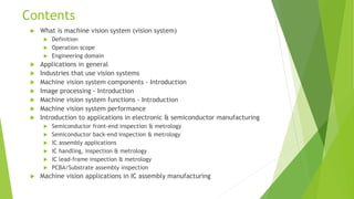
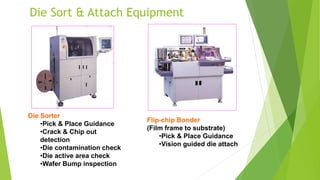
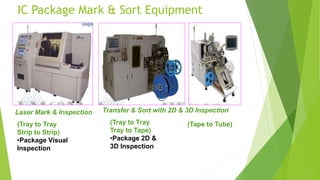
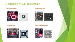
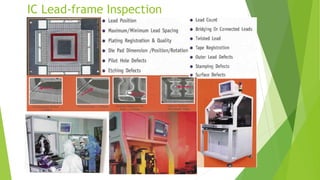
Machine Vision Systems &
Applications In Semiconductor
Manufacturing
Francy Abraham, MSEE, MBA
Sr. Member IEEE
Sr. Member SME-MVA
francy.abraham@gmail.com
Contents
 What is machine vision system (vision system)
 Definition
 Operation scope
 Engineering domain
 Applications in general
 Industries that use vision systems
 Machine vision system components - Introduction
 Image processing - Introduction
 Machine vision system functions - Introduction
 Machine vision system performance
 Introduction to applications in electronic & semiconductor manufacturing
 Semiconductor front-end inspection & metrology
 Semiconductor back-end inspection & metrology
 IC assembly applications
 IC handling, inspection & metrology
 IC lead-frame inspection & metrology
 PCBA/Substrate assembly inspection
 Machine vision applications in IC assembly manufacturing
Machine Vision - Introduction
What is machine vision system?
A device & technique for automatic non-
contact acquisition and analysis of images
to obtain desired data for use in
controlling a process or activity
- Perry West
Operation Scope
 Operate beyond Human Vision
IR
UV/DUV
X-ray
Radio UV X-rays Gamma RaysMicrowave Infrared
Human Eye
103
10-12
10nm1500um
Machine Eye
400nm700nm
Sun Light
~250nm~20um
Electromagnetic Spectrum
Machine Vision: Engineering Domain
•Optics/Electro-optics
•Illumination
•CCD/CMOS Cameras
•Frame Grabber
•Computer
•Precision Mechanical Scan
•Precision stages
•Absolute Encoders
•Motion Control
•Image Processing (Software)
•Pixel Count
•Correlation/NC
•Blob Analysis
•Pattern Matching/GP
•Decision Matrix
•Neural Networks
•Fuzzy Logic
•Many more …
Multimedia
Scientific
Imaging
Image
Processing
Machine
Vision
Electronic Imaging
Industries That Use Machine Vision Systems
 Semiconductor
 PCB/A
 Automotive
 Pharmaceutical
 Packaging
 Military
 Electronic Components
 Food Processing
 Medical Device
 Glass
 Primary Metals
(Partial List)
Machine Vision System Applications
 Quality Assurance
 Metrology
 Flaw Detection
 Defect Detection
 Foreign Particles
 Contamination
 Test & Calibration
 Sensor calibration
 Real-Time Process Control
 Optical fiber drawing
 Hot steel strip rolling
 Data Collection & Sorting
 Mail Sort
 Machine Monitoring
 Operation monitoring
 Material Handling
 - Storage, Retrieval, Routing
 Gauging/Metrology
 - Not contact measurement
 Robotic/Machine Guidance
 - Recognize, Locate, Guide
 ID Tracking
 - OCR, 1D & 2D barcode
 Counting
 - Counting bottles Or cans in
a conveyor
 Safety
 - Detect Obstacles and alarm
or stop
 Law Enforcement
 Vehicle tracking
 Electronic Road Pricing
Machine Vision System Components
 Single or array of sensors to detect
electromagnetic energy, usually 2D array
 Mechanism to collect
reflected/transmitted energy
 Image formation hardware/electro-opto-
mechanical assemblies
 Image acquisition hardware
 Image processing hardware & software
 I/O interfaces & User Interfaces
 Data communication
Images in Machine Vision Systems
 Two dimensional array
 Each element is called a pixel
 Each pixel is a representation of
 surface information – 2D
 Height information – 3D (Voxel)
 The information can be
 Visual
 Non Visual
 Each pixel normally has a integer value (0 - 255) for 8
bit
 There are images with 10bit, 12bit, 16bit or 24 bit pixel
resolutions
 The co-ordinate system has origin at top left corner
Image Processing Methods
 Pixel Counting
 Thresholding
 Connectivity & segmentation
 Blob analysis
 Edge Detection
 Template Matching
 Pattern Recognition
 Optical Character Recognition (OCR)
 Barcode Reading – 1D, 2D codes
Machine Vision System Functions
 Location &
Orientation
 Gauging/Metrology
 Inspection/ Flaw
Detection
 Verification
 Identification
 Recognition
 Tracking & Guidance
Machine Vision System Performance
 Perform Beyond Human Vision
 High Speed
 High Magnification/Resolution
 Highly Repeatable in controlled environment
 No fatigue - 24/7
 Reliable
 Cheaper
 Good for unsafe and hazardous environment
 Operate well in space constrained environments
Semiconductor: Front-end Applications
•SEM
•Ellipsometer
•Reflectometer
•X-ray Fluroscence
•Interferometer
•Wave-front Sensing
•Dark Field Imaging
Semiconductor: Macro-inspection Applications
• On-the-fly inspection
• Template matching, blob Analysis, pixel counting
• Laser triangulation
• High speed con-focal Imaging
• Interferometer
Applications In IC Assembly Manufacturing
Auto-alignment
Auto Pick-n-Place
Inspection
2D DM Reader
Die Sort & Attach Equipment
Die Sorter
•Pick & Place Guidance
•Crack & Chip out
detection
•Die contamination check
•Die active area check
•Wafer Bump inspection
Flip-chip Bonder
(Film frame to substrate)
•Pick & Place Guidance
•Vision guided die attach
Die Bonder & Wire Bonder
Die Bonder
•Pad Location &
alignment
•Glue Metrology
•Die placement
•Die position check
Wire Bonder
•Locate and align die
pad and leadframe pad
position
IC Package Mark & Sort Equipment
Laser Mark & Inspection Transfer & Sort with 2D & 3D Inspection
(Tray to Tray
Strip to Strip)
•Package Visual
Inspection
(Tray to Tray
Tray to Tape)
•Package 2D &
3D Inspection
(Tape to Tube)
IC Package Visual Inspection
IC Package, Lead, Ball Inspection
•Contamination
•Package size
•Pin1 marking
•Orientation
•OCV
•Cracks
•Chip out
•Warpage
•Lead pitch/bend
•Sweep
•Lead co-planarity
•Lead length
•Lead width
•Stand off
•Missing Ball
•Over sized ball
•Under sized ball
•Extra ball
•Ball residue
•Ball Height
•Co planarity
IC Lead-frame Inspection
PCBA/Substrate Inspection
Thank You
francy.abraham@gmail.com

Machine Vision Systems And Applications

  • 1.
    Machine Vision Systems& Applications In Semiconductor Manufacturing Francy Abraham, MSEE, MBA Sr. Member IEEE Sr. Member SME-MVA francy.abraham@gmail.com
  • 2.
    Contents  What ismachine vision system (vision system)  Definition  Operation scope  Engineering domain  Applications in general  Industries that use vision systems  Machine vision system components - Introduction  Image processing - Introduction  Machine vision system functions - Introduction  Machine vision system performance  Introduction to applications in electronic & semiconductor manufacturing  Semiconductor front-end inspection & metrology  Semiconductor back-end inspection & metrology  IC assembly applications  IC handling, inspection & metrology  IC lead-frame inspection & metrology  PCBA/Substrate assembly inspection  Machine vision applications in IC assembly manufacturing
  • 3.
    Machine Vision -Introduction What is machine vision system? A device & technique for automatic non- contact acquisition and analysis of images to obtain desired data for use in controlling a process or activity - Perry West
  • 4.
    Operation Scope  Operatebeyond Human Vision IR UV/DUV X-ray Radio UV X-rays Gamma RaysMicrowave Infrared Human Eye 103 10-12 10nm1500um Machine Eye 400nm700nm Sun Light ~250nm~20um Electromagnetic Spectrum
  • 5.
    Machine Vision: EngineeringDomain •Optics/Electro-optics •Illumination •CCD/CMOS Cameras •Frame Grabber •Computer •Precision Mechanical Scan •Precision stages •Absolute Encoders •Motion Control •Image Processing (Software) •Pixel Count •Correlation/NC •Blob Analysis •Pattern Matching/GP •Decision Matrix •Neural Networks •Fuzzy Logic •Many more … Multimedia Scientific Imaging Image Processing Machine Vision Electronic Imaging
  • 6.
    Industries That UseMachine Vision Systems  Semiconductor  PCB/A  Automotive  Pharmaceutical  Packaging  Military  Electronic Components  Food Processing  Medical Device  Glass  Primary Metals (Partial List)
  • 7.
    Machine Vision SystemApplications  Quality Assurance  Metrology  Flaw Detection  Defect Detection  Foreign Particles  Contamination  Test & Calibration  Sensor calibration  Real-Time Process Control  Optical fiber drawing  Hot steel strip rolling  Data Collection & Sorting  Mail Sort  Machine Monitoring  Operation monitoring  Material Handling  - Storage, Retrieval, Routing  Gauging/Metrology  - Not contact measurement  Robotic/Machine Guidance  - Recognize, Locate, Guide  ID Tracking  - OCR, 1D & 2D barcode  Counting  - Counting bottles Or cans in a conveyor  Safety  - Detect Obstacles and alarm or stop  Law Enforcement  Vehicle tracking  Electronic Road Pricing
  • 8.
    Machine Vision SystemComponents  Single or array of sensors to detect electromagnetic energy, usually 2D array  Mechanism to collect reflected/transmitted energy  Image formation hardware/electro-opto- mechanical assemblies  Image acquisition hardware  Image processing hardware & software  I/O interfaces & User Interfaces  Data communication
  • 9.
    Images in MachineVision Systems  Two dimensional array  Each element is called a pixel  Each pixel is a representation of  surface information – 2D  Height information – 3D (Voxel)  The information can be  Visual  Non Visual  Each pixel normally has a integer value (0 - 255) for 8 bit  There are images with 10bit, 12bit, 16bit or 24 bit pixel resolutions  The co-ordinate system has origin at top left corner
  • 10.
    Image Processing Methods Pixel Counting  Thresholding  Connectivity & segmentation  Blob analysis  Edge Detection  Template Matching  Pattern Recognition  Optical Character Recognition (OCR)  Barcode Reading – 1D, 2D codes
  • 11.
    Machine Vision SystemFunctions  Location & Orientation  Gauging/Metrology  Inspection/ Flaw Detection  Verification  Identification  Recognition  Tracking & Guidance
  • 12.
    Machine Vision SystemPerformance  Perform Beyond Human Vision  High Speed  High Magnification/Resolution  Highly Repeatable in controlled environment  No fatigue - 24/7  Reliable  Cheaper  Good for unsafe and hazardous environment  Operate well in space constrained environments
  • 13.
    Semiconductor: Front-end Applications •SEM •Ellipsometer •Reflectometer •X-rayFluroscence •Interferometer •Wave-front Sensing •Dark Field Imaging
  • 14.
    Semiconductor: Macro-inspection Applications •On-the-fly inspection • Template matching, blob Analysis, pixel counting • Laser triangulation • High speed con-focal Imaging • Interferometer
  • 15.
    Applications In ICAssembly Manufacturing Auto-alignment Auto Pick-n-Place Inspection 2D DM Reader
  • 16.
    Die Sort &Attach Equipment Die Sorter •Pick & Place Guidance •Crack & Chip out detection •Die contamination check •Die active area check •Wafer Bump inspection Flip-chip Bonder (Film frame to substrate) •Pick & Place Guidance •Vision guided die attach
  • 17.
    Die Bonder &Wire Bonder Die Bonder •Pad Location & alignment •Glue Metrology •Die placement •Die position check Wire Bonder •Locate and align die pad and leadframe pad position
  • 18.
    IC Package Mark& Sort Equipment Laser Mark & Inspection Transfer & Sort with 2D & 3D Inspection (Tray to Tray Strip to Strip) •Package Visual Inspection (Tray to Tray Tray to Tape) •Package 2D & 3D Inspection (Tape to Tube)
  • 19.
  • 20.
    IC Package, Lead,Ball Inspection •Contamination •Package size •Pin1 marking •Orientation •OCV •Cracks •Chip out •Warpage •Lead pitch/bend •Sweep •Lead co-planarity •Lead length •Lead width •Stand off •Missing Ball •Over sized ball •Under sized ball •Extra ball •Ball residue •Ball Height •Co planarity
  • 21.
  • 22.
  • 23.