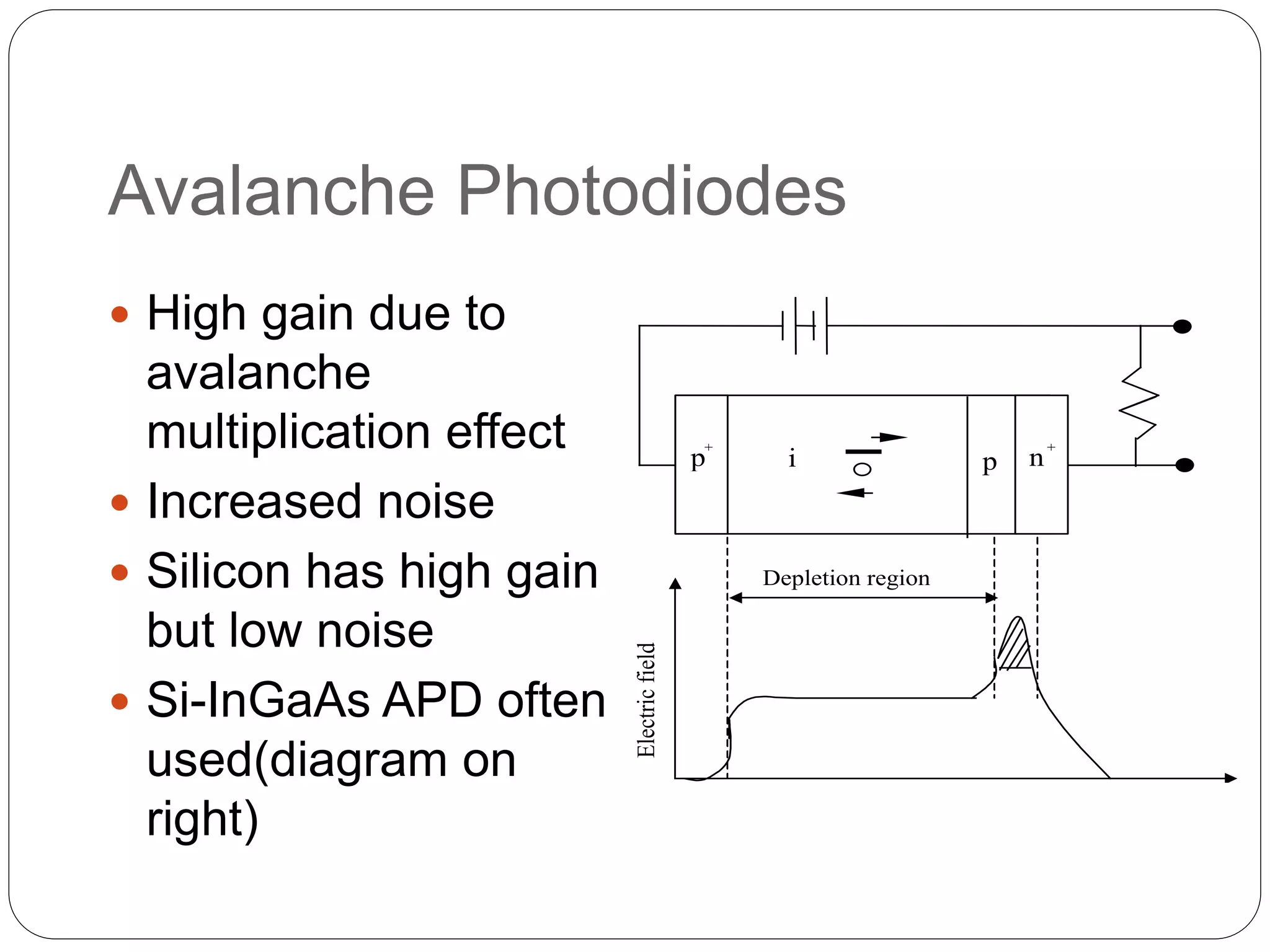
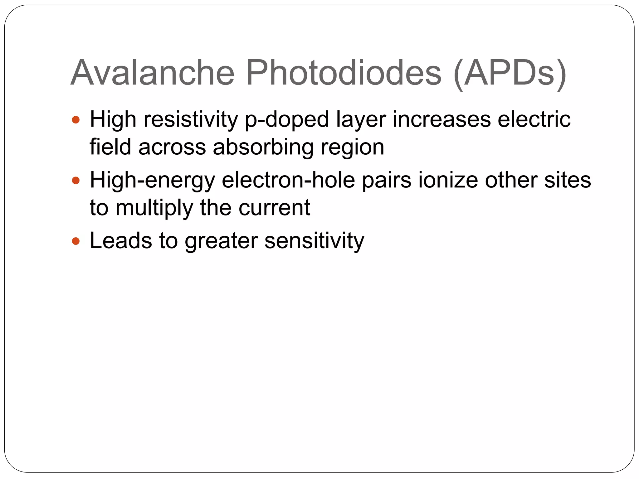
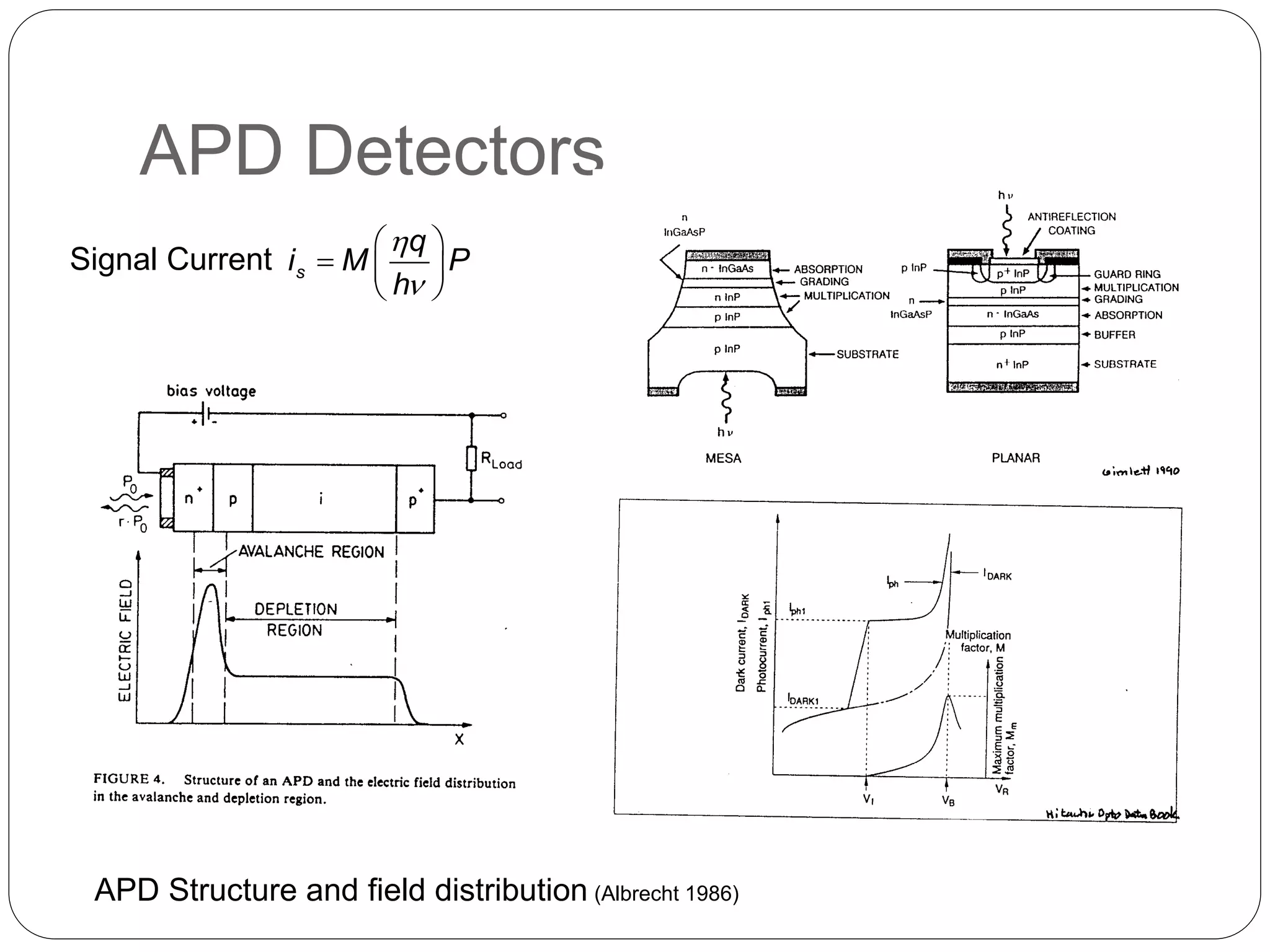
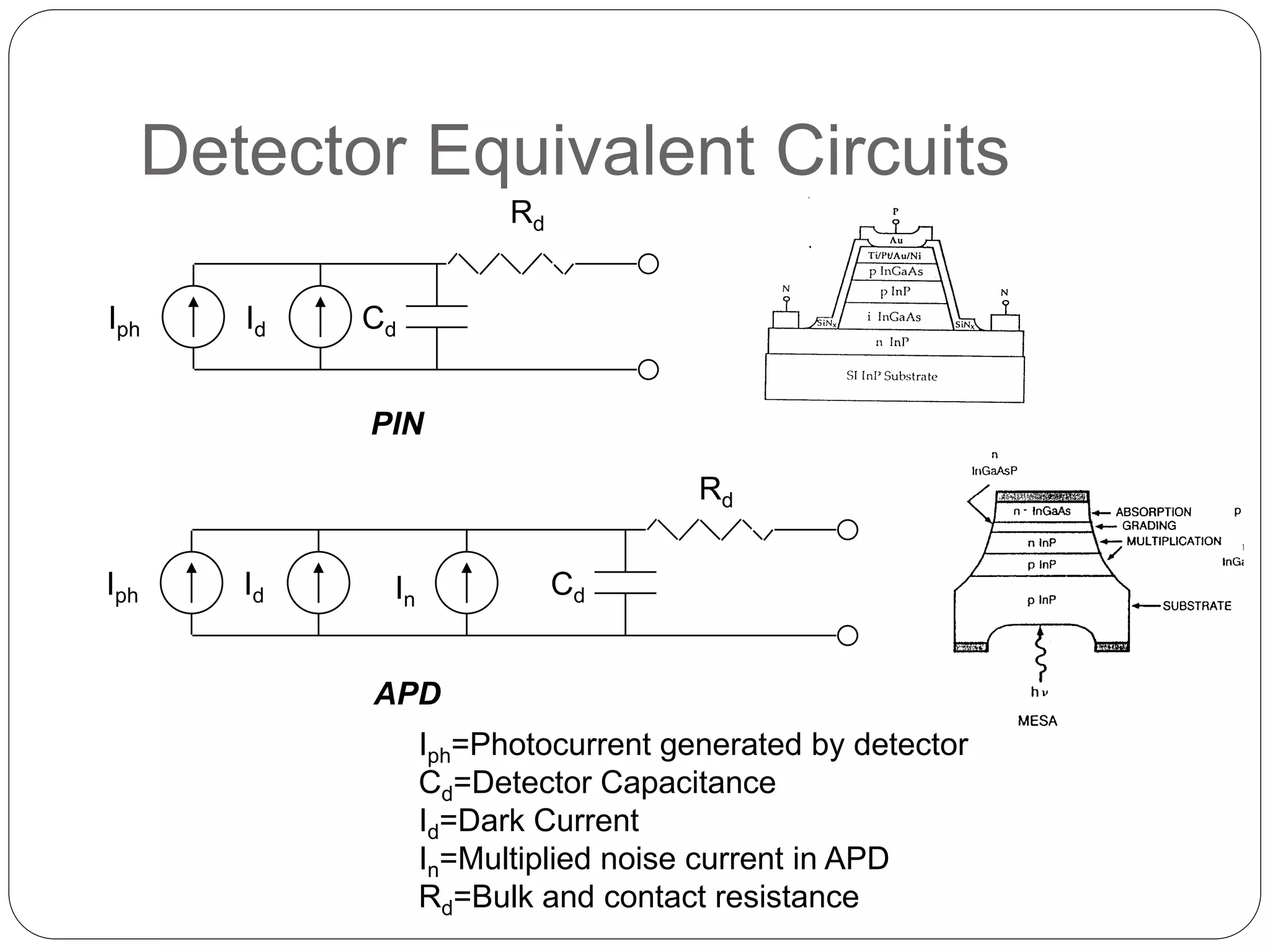
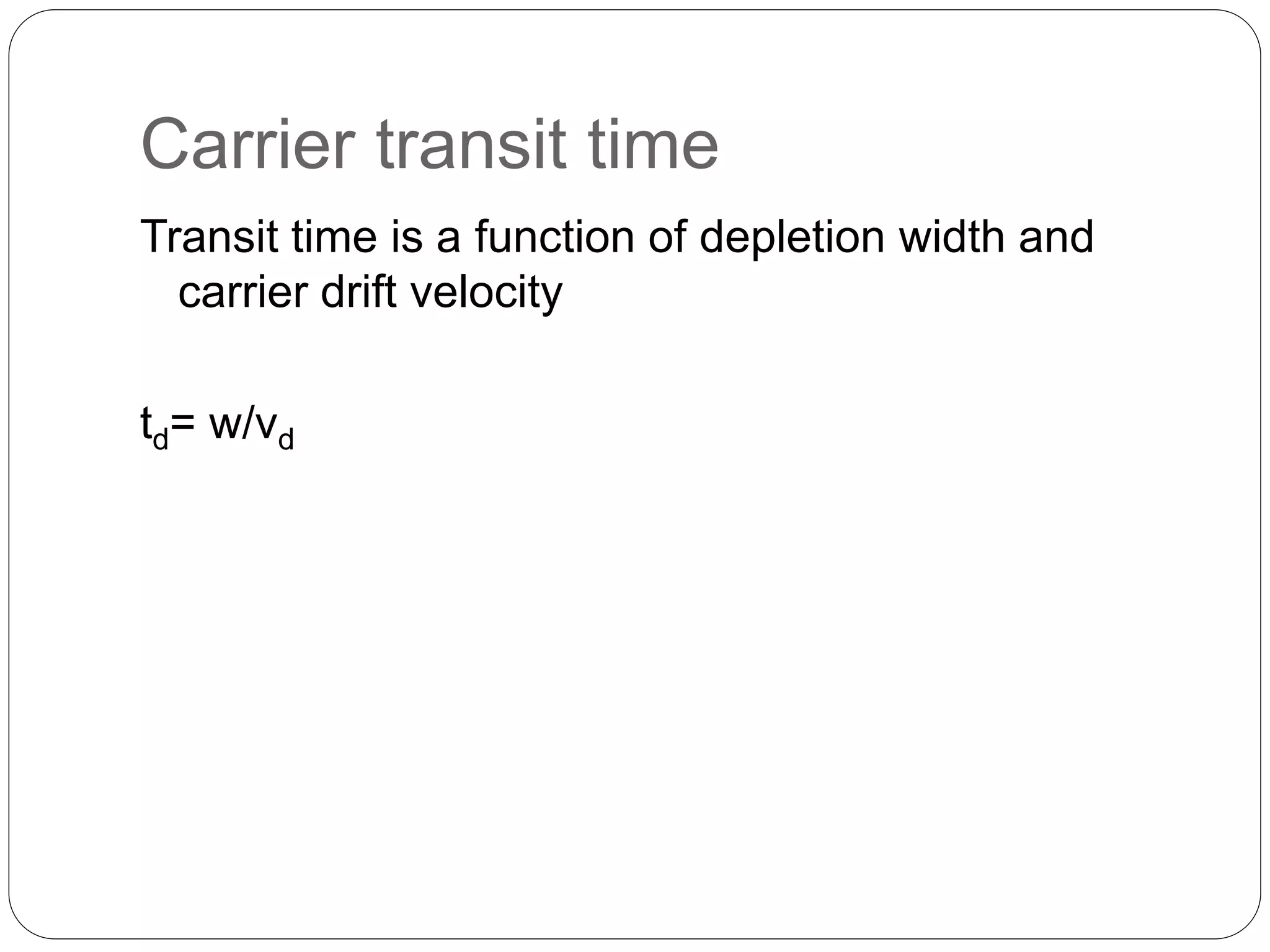
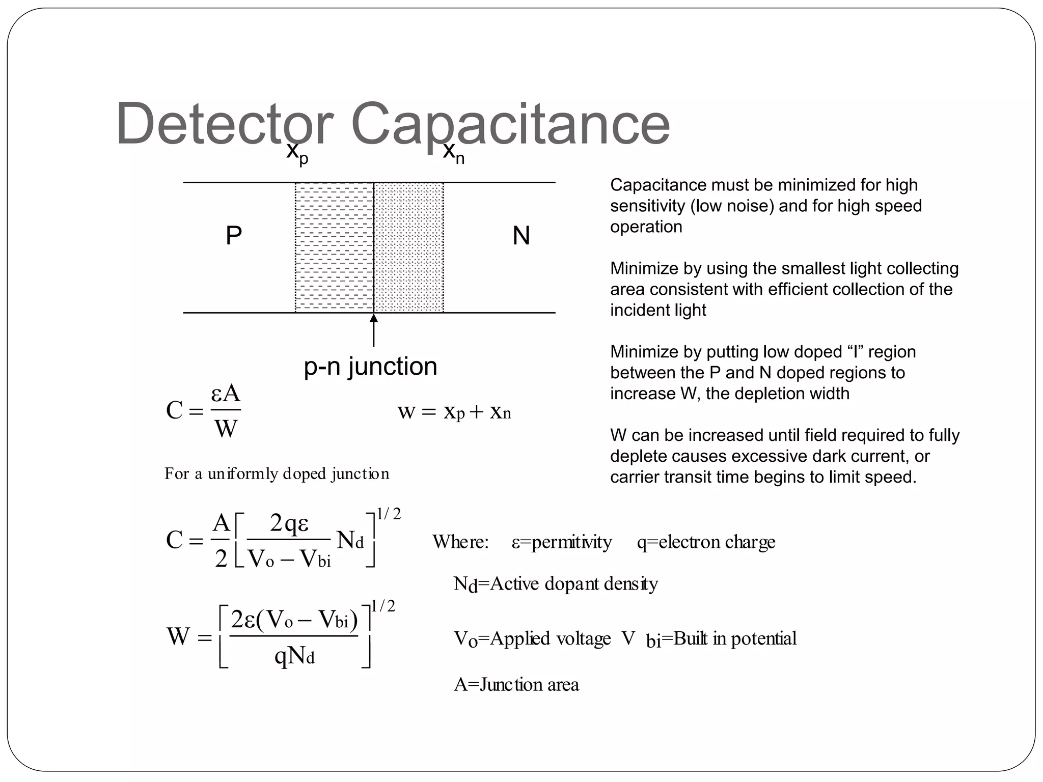
PRESENTED BY:-
BHUPESH SHARMA
ROLL NO : 15S/EL017
AVALANCHE PHOTODIODE &
THERE BANDWIDTH
INTRODUCTION
 The performance of Avalanche photo diode depends upon
the efficiency.
 It convert light energy in to electrical signal.
PRINCIPLE
 Designed to operate in reverse bias condition.
 Photo electric effect:
Avalanche Photodiodes
 High gain due to
avalanche
multiplication effect
 Increased noise
 Silicon has high gain
but low noise
 Si-InGaAs APD often
used(diagram on
right)
n
+
p
+
pi
Electricfield
Depletion region
Avalanche Photodiodes (APDs)
 High resistivity p-doped layer increases electric
field across absorbing region
 High-energy electron-hole pairs ionize other sites
to multiply the current
 Leads to greater sensitivity
APD Detectors
Signal Current


 
  
 
s
q
i M P
h
APD Structure and field distribution (Albrecht 1986)
Detector Equivalent Circuits
Iph
Rd
Id Cd
PIN
Iph
Rd
Id Cd
APD
In
Iph=Photocurrent generated by detector
Cd=Detector Capacitance
Id=Dark Current
In=Multiplied noise current in APD
Rd=Bulk and contact resistance
Carrier transit time
Transit time is a function of depletion width and
carrier drift velocity
td= w/vd
Detector Capacitance
p-n junction
xp xn
For a uniformly doped junction
Where: =permitivity q=electron charge
Nd=Active dopant density
Vo=Applied voltage V bi=Built in potential
A=Junction area
C 
A
W
w  xp  xn
C 
A
2
2q
Vo  Vbi
Nd




1/ 2
W 
2(Vo  Vbi)
qNd




1/2
P N
Capacitance must be minimized for high
sensitivity (low noise) and for high speed
operation
Minimize by using the smallest light collecting
area consistent with efficient collection of the
incident light
Minimize by putting low doped “I” region
between the P and N doped regions to
increase W, the depletion width
W can be increased until field required to fully
deplete causes excessive dark current, or
carrier transit time begins to limit speed.
Bandwidth limit
C=0K A/w
where K is dielectric constant, A is area, w is
depletion width, and 0 is the permittivity of free
space (8.85 pF/m)
B = 1/2RC
MERITS
 APD
 Large gain
 Greater level of sensitivity
 High speed
DEMERITS
 Much higher operating voltage required
 Much higher level of noise
 Output is not linear
 Requires high reverse bias for operation
 Not as widely used due to low reliability
APPLICATION
 Level of gain is of importance for high voltage
requirement.
 Laser range finders
 Fast receiver modules for data communications
 High speed laser scanner (2D bar code reader)
 Speed gun

Avalanche photodiode & there bandwidth

  • 1.
    PRESENTED BY:- BHUPESH SHARMA ROLLNO : 15S/EL017 AVALANCHE PHOTODIODE & THERE BANDWIDTH
  • 2.
    INTRODUCTION  The performanceof Avalanche photo diode depends upon the efficiency.  It convert light energy in to electrical signal.
  • 3.
    PRINCIPLE  Designed tooperate in reverse bias condition.  Photo electric effect:
  • 4.
    Avalanche Photodiodes  Highgain due to avalanche multiplication effect  Increased noise  Silicon has high gain but low noise  Si-InGaAs APD often used(diagram on right) n + p + pi Electricfield Depletion region
  • 5.
    Avalanche Photodiodes (APDs) High resistivity p-doped layer increases electric field across absorbing region  High-energy electron-hole pairs ionize other sites to multiply the current  Leads to greater sensitivity
  • 6.
    APD Detectors Signal Current         s q i M P h APD Structure and field distribution (Albrecht 1986)
  • 7.
    Detector Equivalent Circuits Iph Rd IdCd PIN Iph Rd Id Cd APD In Iph=Photocurrent generated by detector Cd=Detector Capacitance Id=Dark Current In=Multiplied noise current in APD Rd=Bulk and contact resistance
  • 8.
    Carrier transit time Transittime is a function of depletion width and carrier drift velocity td= w/vd
  • 9.
    Detector Capacitance p-n junction xpxn For a uniformly doped junction Where: =permitivity q=electron charge Nd=Active dopant density Vo=Applied voltage V bi=Built in potential A=Junction area C  A W w  xp  xn C  A 2 2q Vo  Vbi Nd     1/ 2 W  2(Vo  Vbi) qNd     1/2 P N Capacitance must be minimized for high sensitivity (low noise) and for high speed operation Minimize by using the smallest light collecting area consistent with efficient collection of the incident light Minimize by putting low doped “I” region between the P and N doped regions to increase W, the depletion width W can be increased until field required to fully deplete causes excessive dark current, or carrier transit time begins to limit speed.
  • 10.
    Bandwidth limit C=0K A/w whereK is dielectric constant, A is area, w is depletion width, and 0 is the permittivity of free space (8.85 pF/m) B = 1/2RC
  • 11.
    MERITS  APD  Largegain  Greater level of sensitivity  High speed
  • 12.
    DEMERITS  Much higheroperating voltage required  Much higher level of noise  Output is not linear  Requires high reverse bias for operation  Not as widely used due to low reliability
  • 13.
    APPLICATION  Level ofgain is of importance for high voltage requirement.  Laser range finders  Fast receiver modules for data communications  High speed laser scanner (2D bar code reader)  Speed gun