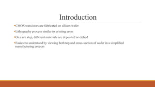
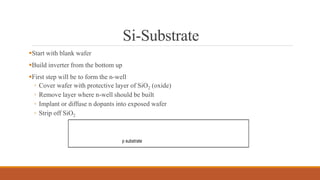
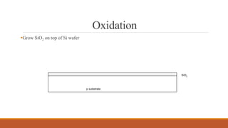
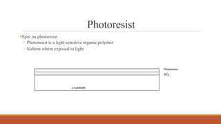
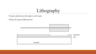
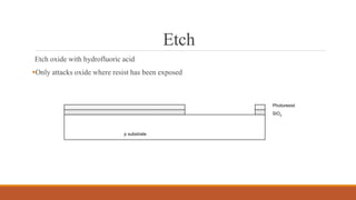
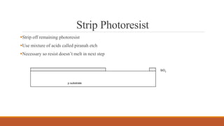
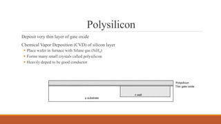
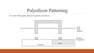
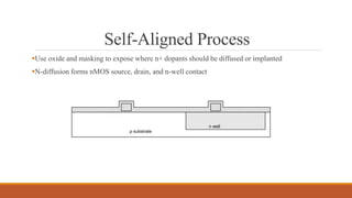
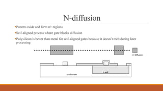
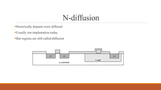
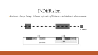
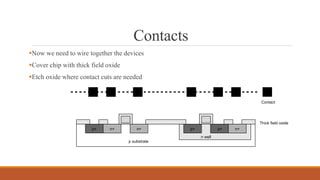
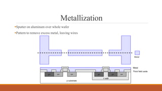
CMOS Fabrication
T.KANAGARAJ
ASSISTANT PROFESSOR / ECE
KIT - KALAIGNARKARUNANIDHI INSTITUTE OF TECHNOLOGY
Introduction
CMOS transistors are fabricated on silicon wafer
Lithography process similar to printing press
On each step, different materials are deposited or etched
Easiest to understand by viewing both top and cross-section of wafer in a simplified
manufacturing process
Si-Substrate
Start with blank wafer
Build inverter from the bottom up
First step will be to form the n-well
◦ Cover wafer with protective layer of SiO2 (oxide)
◦ Remove layer where n-well should be built
◦ Implant or diffuse n dopants into exposed wafer
◦ Strip off SiO2
p substrate
Oxidation
Grow SiO2 on top of Si wafer
p substrate
SiO2
Photoresist
Spin on photoresist
◦ Photoresist is a light-sensitive organic polymer
◦ Softens where exposed to light
p substrate
SiO2
Photoresist
Lithography
Expose photoresist through n-well mask
Strip off exposed photoresist
p substrate
SiO2
Photoresist
Etch
Etch oxide with hydrofluoric acid
Only attacks oxide where resist has been exposed
p substrate
SiO2
Photoresist
Strip Photoresist
Strip off remaining photoresist
Use mixture of acids called piranah etch
Necessary so resist doesn’t melt in next step
p substrate
SiO2
n-well
n-well is formed with diffusion or ion implantation
Diffusion
 Place wafer in furnace with arsenic gas
 Heat until As atoms diffuse into exposed Si
Ion Implanatation
 Blast wafer with beam of As ions
 Ions blocked by SiO2, only enter exposed Si
n well
SiO2
Strip Oxide
Strip off the remaining oxide using HF
Back to bare wafer with n-well
Subsequent steps involve similar series of steps
p substrate
n well
Polysilicon
Deposit very thin layer of gate oxide
Chemical Vapor Deposition (CVD) of silicon layer
 Place wafer in furnace with Silane gas (SiH4)
 Forms many small crystals called polysilicon
 Heavily doped to be good conductor
Thin gate oxide
Polysilicon
p substrate
n well
Polysilicon Patterning
Use same lithography process to pattern polysilicon
Polysilicon
p substrate
Thin gate oxide
Polysilicon
n well
Self-Aligned Process
Use oxide and masking to expose where n+ dopants should be diffused or implanted
N-diffusion forms nMOS source, drain, and n-well contact
p substrate
n well
N-diffusion
Pattern oxide and form n+ regions
Self-aligned process where gate blocks diffusion
Polysilicon is better than metal for self-aligned gates because it doesn’t melt during later
processing
p substrate
n well
n+ Diffusion
N-diffusion
Historically dopants were diffused
Usually ion implantation today
But regions are still called diffusion
n well
p substrate
n+n+ n+
P-Diffusion
Similar set of steps form p+ diffusion regions for pMOS source and drain and substrate contact
p+ Diffusion
p substrate
n well
n+n+ n+p+p+p+
Contacts
Now we need to wire together the devices
Cover chip with thick field oxide
Etch oxide where contact cuts are needed
p substrate
Thick field oxide
n well
n+n+ n+p+p+p+
Contact
Metallization
Sputter on aluminum over whole wafer
Pattern to remove excess metal, leaving wires
p substrate
Metal
Thick field oxide
n well
n+n+ n+p+p+p+
Metal
Summary
MOS Transistors are stack of gate, oxide, silicon
Can be viewed as electrically controlled switches
Build logic gates out of switches
Draw masks to specify layout of transistors
Thank You..

Cmos fabrication

  • 1.
    CMOS Fabrication T.KANAGARAJ ASSISTANT PROFESSOR/ ECE KIT - KALAIGNARKARUNANIDHI INSTITUTE OF TECHNOLOGY
  • 2.
    Introduction CMOS transistors arefabricated on silicon wafer Lithography process similar to printing press On each step, different materials are deposited or etched Easiest to understand by viewing both top and cross-section of wafer in a simplified manufacturing process
  • 3.
    Si-Substrate Start with blankwafer Build inverter from the bottom up First step will be to form the n-well ◦ Cover wafer with protective layer of SiO2 (oxide) ◦ Remove layer where n-well should be built ◦ Implant or diffuse n dopants into exposed wafer ◦ Strip off SiO2 p substrate
  • 4.
    Oxidation Grow SiO2 ontop of Si wafer p substrate SiO2
  • 5.
    Photoresist Spin on photoresist ◦Photoresist is a light-sensitive organic polymer ◦ Softens where exposed to light p substrate SiO2 Photoresist
  • 6.
    Lithography Expose photoresist throughn-well mask Strip off exposed photoresist p substrate SiO2 Photoresist
  • 7.
    Etch Etch oxide withhydrofluoric acid Only attacks oxide where resist has been exposed p substrate SiO2 Photoresist
  • 8.
    Strip Photoresist Strip offremaining photoresist Use mixture of acids called piranah etch Necessary so resist doesn’t melt in next step p substrate SiO2
  • 9.
    n-well n-well is formedwith diffusion or ion implantation Diffusion  Place wafer in furnace with arsenic gas  Heat until As atoms diffuse into exposed Si Ion Implanatation  Blast wafer with beam of As ions  Ions blocked by SiO2, only enter exposed Si n well SiO2
  • 10.
    Strip Oxide Strip offthe remaining oxide using HF Back to bare wafer with n-well Subsequent steps involve similar series of steps p substrate n well
  • 11.
    Polysilicon Deposit very thinlayer of gate oxide Chemical Vapor Deposition (CVD) of silicon layer  Place wafer in furnace with Silane gas (SiH4)  Forms many small crystals called polysilicon  Heavily doped to be good conductor Thin gate oxide Polysilicon p substrate n well
  • 12.
    Polysilicon Patterning Use samelithography process to pattern polysilicon Polysilicon p substrate Thin gate oxide Polysilicon n well
  • 13.
    Self-Aligned Process Use oxideand masking to expose where n+ dopants should be diffused or implanted N-diffusion forms nMOS source, drain, and n-well contact p substrate n well
  • 14.
    N-diffusion Pattern oxide andform n+ regions Self-aligned process where gate blocks diffusion Polysilicon is better than metal for self-aligned gates because it doesn’t melt during later processing p substrate n well n+ Diffusion
  • 15.
    N-diffusion Historically dopants werediffused Usually ion implantation today But regions are still called diffusion n well p substrate n+n+ n+
  • 16.
    P-Diffusion Similar set ofsteps form p+ diffusion regions for pMOS source and drain and substrate contact p+ Diffusion p substrate n well n+n+ n+p+p+p+
  • 17.
    Contacts Now we needto wire together the devices Cover chip with thick field oxide Etch oxide where contact cuts are needed p substrate Thick field oxide n well n+n+ n+p+p+p+ Contact
  • 18.
    Metallization Sputter on aluminumover whole wafer Pattern to remove excess metal, leaving wires p substrate Metal Thick field oxide n well n+n+ n+p+p+p+ Metal
  • 19.
    Summary MOS Transistors arestack of gate, oxide, silicon Can be viewed as electrically controlled switches Build logic gates out of switches Draw masks to specify layout of transistors
  • 20.