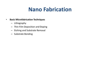
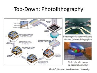
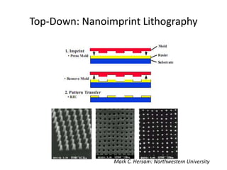
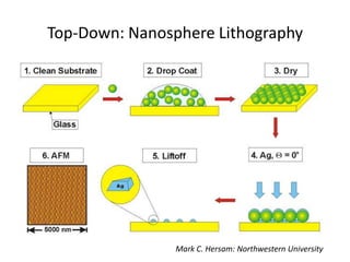
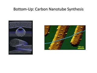
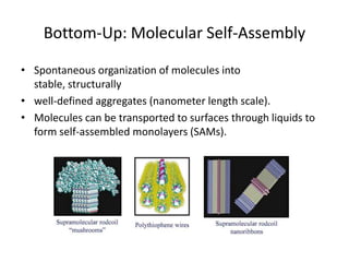
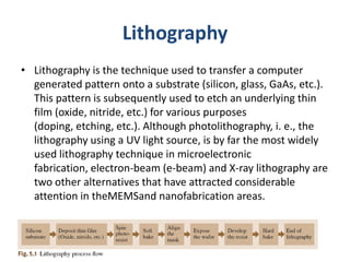
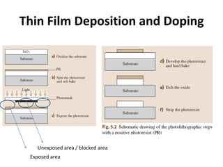
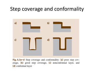
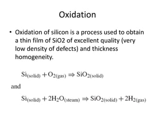
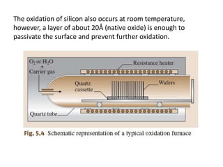
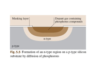
ETE444/544 :: Lecture 5Introduction to Micro FabricationChapter 5Springer Handbook of Nanotechnology (Page 147-)
IntroductionRecent innovations in the area of micro fabrication have created a unique opportunity for manufacturing structures in the nanometer–millimeter range. We can fabricate novel electronic, optical, magnetic, mechanical, and chemical/biological devices with applications ranging from sensors to computation and control.
NanoFabricationBasic Microfabrication TechniquesLithographyThin Film Deposition and DopingEtching and Substrate RemovalSubstrate Bonding
FabricationTop-down: Chisel away material to make nanoscale objectsBottom-up: Assemble nanoscale objects out of even smaller units (e.g., atoms and molecules)Ultimate Goal: Dial in the properties that you want by designing and building at the scale of nature (i.e., the nanoscale)
Top-Down: PhotolithographyMark C. Hersam: Northwestern University
Top-Down: Nanoimprint LithographyMark C. Hersam: Northwestern University
Top-Down: Nanosphere LithographyMark C. Hersam: Northwestern University
Bottom-Up: Carbon Nanotube Synthesis
Bottom-Up: Molecular Self-AssemblySpontaneous organization of molecules into stable, structurallywell-defined aggregates (nanometer length scale).Molecules can be transported to surfaces through liquids to form self-assembled monolayers (SAMs).
 Merging of two approaches: Top-down and bottom-up machining methodologiesMost human manufacturing methods of small devices involve top-down approaches. Starting from larger blocks of material we make smaller and smaller things. Nature works the other way, i.e., from the bottom-up. All living things are made atom by atom , molecule by molecule; from the small to the large. As manufacturing of very small things with top-down techniques  (NEMS or nano mechanical devices) become too expensive or hit other barriers we are looking at nature for guidance (biomimetics).Further miniaturization might be inspired by biology but will most likely be different again from nature  -- the drivers for  human and natural manufacturing techniques are very different.
 Merging of two approaches: Top-down and bottom-up machining methodologies --NEMSMEMS’ little brother is NEMS, the top-down approach to nano devices. This biomimetic approach to nano devices  I like to call nanochemistry. To succeed in the latter we will need  :
self-assembly and directed assembly (e.,g, using electrical fields -see next viewgraph)
massive parallelism
understanding of molecular mechanisms--chemomechanics
engineers/scientists who understand ‘wet’ and ‘dry’ disciplines
Example nano chemistry approaches:
Natural polymers: e.g., NAs and proteins not only as sensors but also as actuators and building blocks (Genetic engineer NA’s and proteins-rely on extremophiles for guidance)
Mechanosynthesis
NEMS/biology hybrids --to learn onlySeemanEiglerDaunert - MadouMontemagno
LithographyLithography is the technique used to transfer a computer generated pattern onto a substrate (silicon, glass, GaAs, etc.). This pattern is subsequently used to etch an underlying thin film (oxide, nitride, etc.) for various purposes (doping, etching, etc.). Although photolithography, i. e., the lithography using a UV light source, is by far the most widely used lithography technique in microelectronic fabrication, electron-beam (e-beam) and X-ray lithography are two other alternatives that have attracted considerable attention in theMEMSand nanofabrication areas.
exposure systemsDepending on the separation between the mask and the wafer, three different exposure systems are available:Contact : gives better resolution than proximity.ProximityProjectionuses a dual lens optical system to project the mask image onto the wafer. Widely used system in microfabrication and can yield superior resolutions compared to contact and proximity methods
Thin Film Deposition and DopingUnexposed area / blocked areaExposed area
Step coverage and conformality
OxidationOxidation of silicon is a process used to obtain a thin film of SiO2 of excellent quality (very low density of defects) and thickness homogeneity.
The oxidation of silicon also occurs at room temperature, however, a layer of about 20Å (native oxide) is enough to passivate the surface and prevent further oxidation.
DopingThe introduction of certain impurities in a semiconductor can change its electrical, chemical, and even mechanical properties. Typical impurities, or dopants, used in silicon include boron (to form p-type regions) and phosphorous or arsenic (to form n-type regions). Doping is the main process used in the microelectronic industry to fabricate major components such as diodes and transistors.
Chemical Vapor Deposition and EpitaxyReaction of chemicals in a gas phase to form the deposited thin filmLPCVD (lowpressureCVD) PECVD (plasma enhanced CVD).
LPCVDLPCVD process is typically carried out in electrically heated tubes, similar to the oxidation tubes, equipped with pumping capabilities to achieve the needed low pressures (0.1 to 1.0 torr). A large number of wafers can be processed simultaneously, and the material is deposited in both sides of the wafers. The process temperatures depend on the material to be deposited, but generally are in the range of 550 to 900 ◦C. As in the oxidation, high temperatures and contamination issues can restrict the type of processes used prior to the LPCVD. Typical materials deposited by LPCVD include silicon oxide (e.g., SiCl2H2 + 2N2O⇒SiO2+2N2+2HCl at 900 ◦C)
PECVDThe PECVD process is performed in plasma systems such as the one represented in Fig. The use of RF energy to create highly reactive species in the plasma allows for the use of lower temperatures at the substrates (150 to 350 ◦C). Parallel-plate plasma reactors normally used in microfabrication can only process a limited number of wafers per batch. The wafers are positioned horizontally on top of the lower electrode, so only one side gets deposited. Typical materials deposited with PECVD include silicon oxide, nitride, and amorphous silicon. Conformality is good for low-aspect-ratio structures, but becomes very poor for deep trenches (20% of the surface thickness inside through-wafer holes with aspect ratio of ten).
Epitaxial growthIn this process, a single crystalline material is grown as an extension of the crystal structure of the substrate.It is possible to grow dissimilar materials if the crystal structures are somehow similar (lattice-matched).Silicon-on-sapphire (SOS) substrates and some heterostructures are fabricated in this way.

ETE444-lec5-micro-fabrication.pptx

  • 1.
    ETE444/544 :: Lecture5Introduction to Micro FabricationChapter 5Springer Handbook of Nanotechnology (Page 147-)
  • 2.
    IntroductionRecent innovations inthe area of micro fabrication have created a unique opportunity for manufacturing structures in the nanometer–millimeter range. We can fabricate novel electronic, optical, magnetic, mechanical, and chemical/biological devices with applications ranging from sensors to computation and control.
  • 3.
    NanoFabricationBasic Microfabrication TechniquesLithographyThinFilm Deposition and DopingEtching and Substrate RemovalSubstrate Bonding
  • 4.
    FabricationTop-down: Chisel awaymaterial to make nanoscale objectsBottom-up: Assemble nanoscale objects out of even smaller units (e.g., atoms and molecules)Ultimate Goal: Dial in the properties that you want by designing and building at the scale of nature (i.e., the nanoscale)
  • 5.
    Top-Down: PhotolithographyMark C.Hersam: Northwestern University
  • 6.
    Top-Down: Nanoimprint LithographyMarkC. Hersam: Northwestern University
  • 7.
    Top-Down: Nanosphere LithographyMarkC. Hersam: Northwestern University
  • 8.
  • 9.
    Bottom-Up: Molecular Self-AssemblySpontaneousorganization of molecules into stable, structurallywell-defined aggregates (nanometer length scale).Molecules can be transported to surfaces through liquids to form self-assembled monolayers (SAMs).
  • 10.
    Merging oftwo approaches: Top-down and bottom-up machining methodologiesMost human manufacturing methods of small devices involve top-down approaches. Starting from larger blocks of material we make smaller and smaller things. Nature works the other way, i.e., from the bottom-up. All living things are made atom by atom , molecule by molecule; from the small to the large. As manufacturing of very small things with top-down techniques (NEMS or nano mechanical devices) become too expensive or hit other barriers we are looking at nature for guidance (biomimetics).Further miniaturization might be inspired by biology but will most likely be different again from nature -- the drivers for human and natural manufacturing techniques are very different.
  • 11.
    Merging oftwo approaches: Top-down and bottom-up machining methodologies --NEMSMEMS’ little brother is NEMS, the top-down approach to nano devices. This biomimetic approach to nano devices I like to call nanochemistry. To succeed in the latter we will need :
  • 12.
    self-assembly and directedassembly (e.,g, using electrical fields -see next viewgraph)
  • 13.
  • 14.
    understanding of molecularmechanisms--chemomechanics
  • 15.
    engineers/scientists who understand‘wet’ and ‘dry’ disciplines
  • 16.
  • 17.
    Natural polymers: e.g.,NAs and proteins not only as sensors but also as actuators and building blocks (Genetic engineer NA’s and proteins-rely on extremophiles for guidance)
  • 18.
  • 19.
    NEMS/biology hybrids --tolearn onlySeemanEiglerDaunert - MadouMontemagno
  • 20.
    LithographyLithography is thetechnique used to transfer a computer generated pattern onto a substrate (silicon, glass, GaAs, etc.). This pattern is subsequently used to etch an underlying thin film (oxide, nitride, etc.) for various purposes (doping, etching, etc.). Although photolithography, i. e., the lithography using a UV light source, is by far the most widely used lithography technique in microelectronic fabrication, electron-beam (e-beam) and X-ray lithography are two other alternatives that have attracted considerable attention in theMEMSand nanofabrication areas.
  • 21.
    exposure systemsDepending onthe separation between the mask and the wafer, three different exposure systems are available:Contact : gives better resolution than proximity.ProximityProjectionuses a dual lens optical system to project the mask image onto the wafer. Widely used system in microfabrication and can yield superior resolutions compared to contact and proximity methods
  • 22.
    Thin Film Depositionand DopingUnexposed area / blocked areaExposed area
  • 23.
    Step coverage andconformality
  • 24.
    OxidationOxidation of siliconis a process used to obtain a thin film of SiO2 of excellent quality (very low density of defects) and thickness homogeneity.
  • 25.
    The oxidation ofsilicon also occurs at room temperature, however, a layer of about 20Å (native oxide) is enough to passivate the surface and prevent further oxidation.
  • 26.
    DopingThe introduction ofcertain impurities in a semiconductor can change its electrical, chemical, and even mechanical properties. Typical impurities, or dopants, used in silicon include boron (to form p-type regions) and phosphorous or arsenic (to form n-type regions). Doping is the main process used in the microelectronic industry to fabricate major components such as diodes and transistors.
  • 28.
    Chemical Vapor Depositionand EpitaxyReaction of chemicals in a gas phase to form the deposited thin filmLPCVD (lowpressureCVD) PECVD (plasma enhanced CVD).
  • 29.
    LPCVDLPCVD process istypically carried out in electrically heated tubes, similar to the oxidation tubes, equipped with pumping capabilities to achieve the needed low pressures (0.1 to 1.0 torr). A large number of wafers can be processed simultaneously, and the material is deposited in both sides of the wafers. The process temperatures depend on the material to be deposited, but generally are in the range of 550 to 900 ◦C. As in the oxidation, high temperatures and contamination issues can restrict the type of processes used prior to the LPCVD. Typical materials deposited by LPCVD include silicon oxide (e.g., SiCl2H2 + 2N2O⇒SiO2+2N2+2HCl at 900 ◦C)
  • 30.
    PECVDThe PECVD processis performed in plasma systems such as the one represented in Fig. The use of RF energy to create highly reactive species in the plasma allows for the use of lower temperatures at the substrates (150 to 350 ◦C). Parallel-plate plasma reactors normally used in microfabrication can only process a limited number of wafers per batch. The wafers are positioned horizontally on top of the lower electrode, so only one side gets deposited. Typical materials deposited with PECVD include silicon oxide, nitride, and amorphous silicon. Conformality is good for low-aspect-ratio structures, but becomes very poor for deep trenches (20% of the surface thickness inside through-wafer holes with aspect ratio of ten).
  • 32.
    Epitaxial growthIn thisprocess, a single crystalline material is grown as an extension of the crystal structure of the substrate.It is possible to grow dissimilar materials if the crystal structures are somehow similar (lattice-matched).Silicon-on-sapphire (SOS) substrates and some heterostructures are fabricated in this way.