Downloaded 439 times
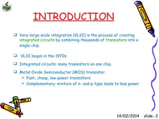
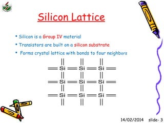
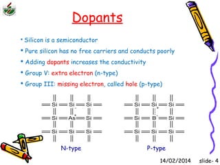
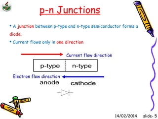
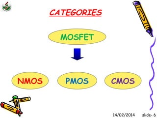
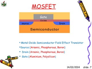

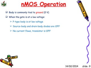

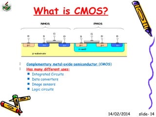
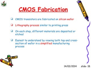


This document is an introduction to CMOS VLSI design and fabrication presented as a slideshow. It begins with an overview of VLSI and MOS transistors, explaining how transistors are built on a silicon substrate and doped to create n-type and p-type semiconductors. It then covers p-n junctions, MOSFET structure, and the operation of nMOS and pMOS transistors. The document introduces CMOS logic gates like inverters built from combinations of nMOS and pMOS transistors. It concludes with an overview of the CMOS fabrication process using lithography and various deposition and etching steps.


