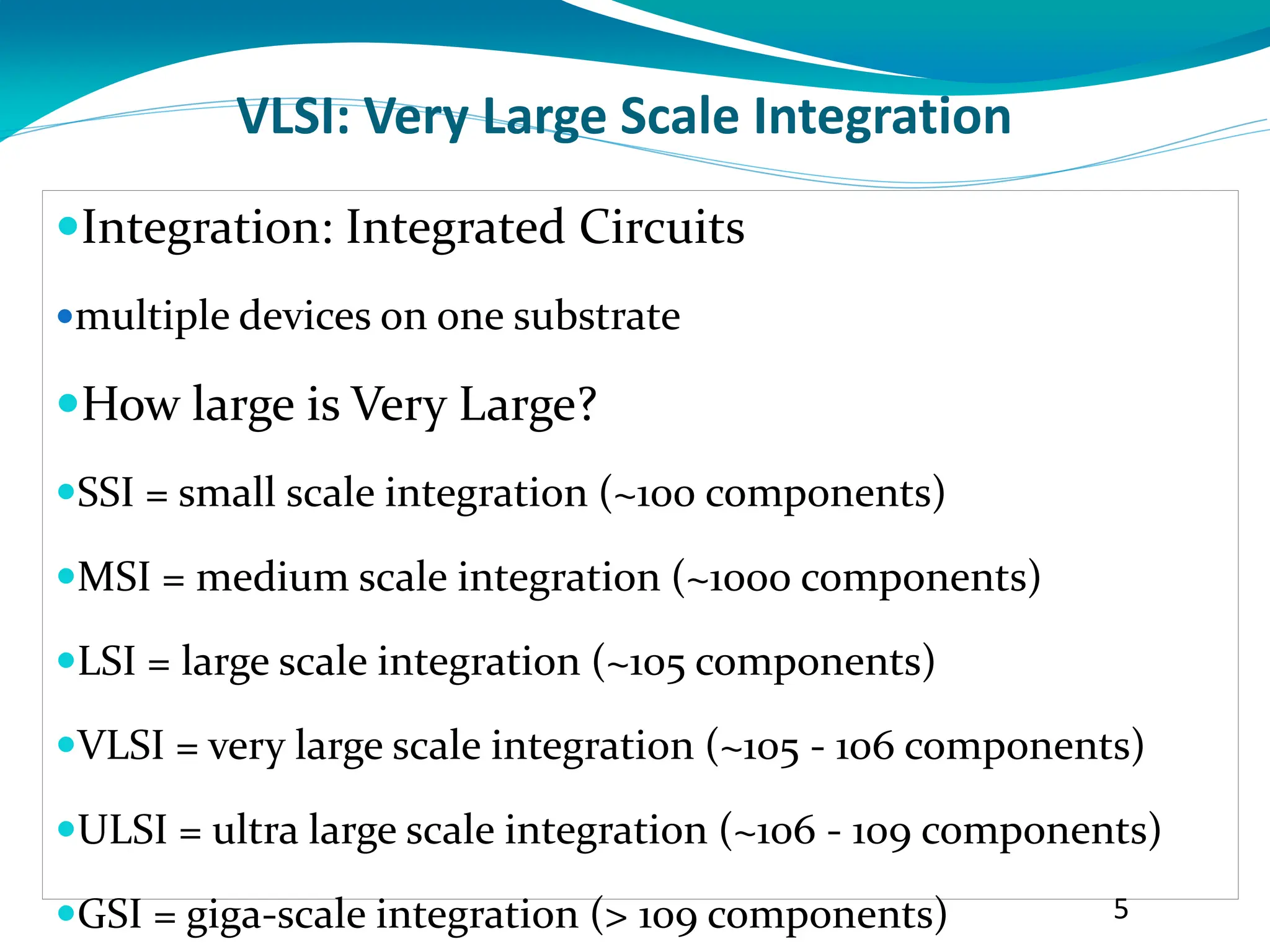
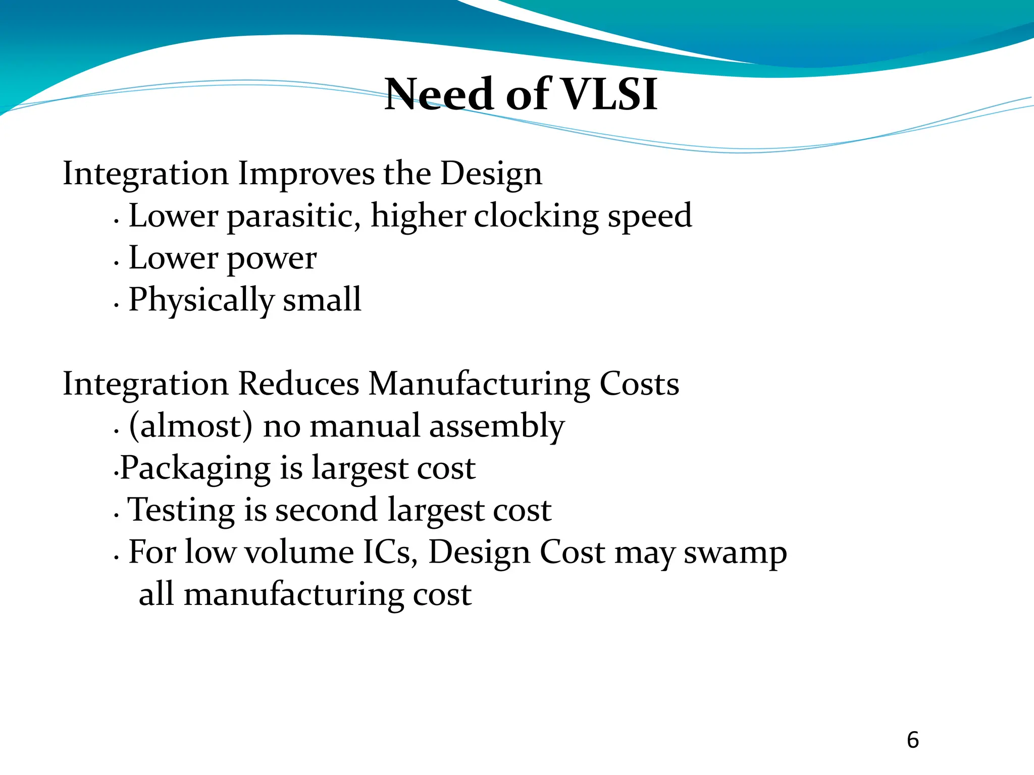
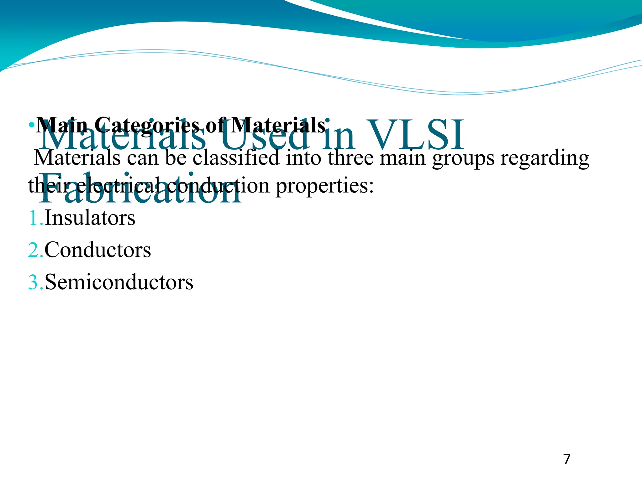
VLSI Technology
Course Syllabus
Unit 1
Cleanroom technology - Clean room concept – Growth of
single crystal Si, surface contamination, Chemical
Mechanical Polishing, wafer preparation, DI water, RCA and
Chemical Cleaning. Processing considerations: Chemical
cleaning, getting the thermal Stress factors etc...
Epitaxy [T1]
Physical Vapour Deposition,phase Epitaxy Basic Transport
processes & reaction kinetics, doping & auto doping,
equipments, & safety considerations, buried layers, epitaxial
defects, molecular beam epitaxy, equipment used, film
characteristics, SOI structure.
Unit 2
• Oxidation [T1]
Growth mechanism & kinetics, Silicon oxidation model,
interface considerations, orientation dependence of 2
Course Syllabus
Diffusion [T1]
Diffusion from a chemical source in vapor form at high
temperature, diffusion from doped oxide source, Ion Implantation,
Annealing and diffusion from an ion implanted layer .
Unit 3
Lithography [T1]
Optical Lithography: optical resists, contact & proximity printing,
projection printing, electron lithography: resists, mask generation.
Electron optics: roster scans & vector scans, variable beam shape.
X-ray lithography: resists & printing, X ray sources & masks. Ion
lithography.
3
Text and Reference Books
Unit 4
Etching [T1]
Reactive plasma etching, AC & DC plasma excitation,
plasma properties, chemistry & surface interactions,
feature size control & apostrophic etching, ion enhanced &
induced etching, properties of etch processing. Reactive
Ion Beam etching, Specific etches processes, Trench
etching.
Metallization
Text Books 4
VLSI: Very Large Scale Integration
Integration: Integrated Circuits
multiple devices on one substrate
How large is Very Large?
SSI = small scale integration (~100 components)
MSI = medium scale integration (~1000 components)
LSI = large scale integration (~105 components)
VLSI = very large scale integration (~105 - 106 components)
ULSI = ultra large scale integration (~106 - 109 components)
GSI = giga-scale integration (> 109 components) 5
Integration Improves the Design
• Lower parasitic, higher clocking speed
• Lower power
• Physically small
Integration Reduces Manufacturing Costs
• (almost) no manual assembly
•Packaging is largest cost
• Testing is second largest cost
• For low volume ICs, Design Cost may swamp
all manufacturing cost
Need of VLSI
6
Materials Used in VLSI
Fabrication
•Main Categories of Materials
Materials can be classified into three main groups regarding
their electrical conduction properties:
1.Insulators
2.Conductors
3.Semiconductors
7
Conductors
•Conductors are used in IC design for electrical connectivity.
The following are good conducting elements:
1.Silver
2.Gold
3.Copper
4.Aluminum
5.Platinum
8
insulators
•Insulators are used to isolate conducting and/or semi-
conducting materials from each other.
•MOS devices and Capacitors rely on an insulator for
their physical operation.
•The choice of the insulators (and the conductors) in IC
design depends heavily on how the materials interact
with each other, especially with the semiconductors.
9
Semiconductors
What are semiconductors?
Materials with electrical conductivities between
conductors and insulators are called semiconductors e.g.Si,
Ge, GaAs, SiC etc.
These are found in group IV and neighboring columns of
the periodic table.
Column IV semiconductors are called elemental as they
are composed of single species of atoms.
Atoms of column III &V, II&VI form compound
semiconductors.
10
Si Material
•The basic semiconductor material used in device
fabrication is Silicon
The success of this material is due to:
•Physical characteristics
•Abundance in nature and very low cost
•Relatively easy to process
•Reliable high volume fabrication
Continued….
Semiconductors may be classified in several
ways.
According to structure they may be
amorphous, polycrystalline or single
crystalline.
Semiconductors may also be classified as
elemental and compound semiconductors.
The electronic and optical properties of
semiconductor materials are strongly
affected by impurities, which may be added
in precisely controlled amounts. These 12
Advantages of Si over Ge
Si has a larger band gap(1.1 eV for Si versus 0.66 eV for
Ge)
Si devices can operate at a higher temperature (150oC
vs100oC)
Intrinsic resistivity is higher (2.3 x 10⁵Ω-cm vs 47 Ω-cm)
SiO2 is more stable than GeO2.
SiO2 is less costly
13
Types of solids
Solids are of three types:-
Amorphous:- which have no periodic structure.
Single crystal:-geometrical periodicity throughout the
material.
Polycrystalline:-with multiple single crystal regions (called
grains) separated by grain boundary.
14
Crystal Structure
Lattice:- A regular periodic array of lattice points in space to
represent the structure of a single crystal.
An important concept:
15
crystal structure = lattice + basis
lattice: a periodic array of points in space. The
environment surrounding each lattice point is
identical.
16
basis: the atom or group of atoms “attached” to each
lattice point in order generate the crystal
structure.
Silicon Disadvantages
Low carrier mobility (m) => slower circuits (compared to
GaAs)
• Indirect band gap: 17
Fabrication Process Flowchart
Growth
Wafer
Film Formation
Lithography
Etching
Diffusion/Ion Implantation
Metallization
Packaging
Impurity Doping
18
Crystal Growth and Wafer
Preparation
19
Wafer
A large wafer diameter enables producing more
Semiconductor devices on a single wafer,
enhancing productivity and efficiency.
Any Silicon’s Die Per Wafer
Flow chart for starting material to
Wafer
Raw Material
Polycrystalline Si
Single Crystal Si
Wafer
Distillation & Reduction
Crystal Growth
Grind, Saw, Polish
Silicon wafer Preparation
Creation of Electronic Grade
Silicon
The process begins with the purification of the starting
material, raw silicon dioxide (silica).
Due to the introduction of impurities in the later stages of
wafer preparation, the refinement of electronic grade silicon
(EGS) from natural silicon dioxide requires the number of
impurities to be reduced to less than one (ppb).
•Refinement process include two methods:-
1. Reduction.
2.Purification.
Sand to Silicon
Reduction: The sand that is used to produce silicon wafers is compose
of mainly silicon dioxide. This can be made to react with carbon at very
high temperatures.(1500-2000˚c)
The carbon replaces silicon to form silicon and carbon monoxide and
carbon dioxide.
The silicon oxygen bond is very strong so a very high temperature
process is needed for this carbon reducing reaction.
This process generates polycrystalline silicon with about 98% purity
and is called “crude silicon” or “metallurgical grade silicon” (MGS).
Crude silicon has a very high impurity concentration and so needs
further refining for use in the semiconductor industry.
2 2 2
Heat
SiO C Si CO
 
 
Reduction
The first step in the refining process involves
reducing the silica (silicon dioxide) into silicon and
carbon monoxide.
This is achieved by heating the raw silica in a furnace
containing an appropriate amount of carbon,
typically in the form of coal, coke, or wood.
98% pure Si is obtained.
Reduction of Silica
Silicon Purification
•Purification of silicon has several steps. First the
crude silicon is ground into a fine powder. The
powder is then fed into a reactor along with HCL
vapour. At ~300ºC trichlorosilane (TCS, SiHCL3)
is produced.
•This TCS vapour is then put through a series of
filters, condensers and purifiers to produce ultra
high purity TCS liquid.
2
3
)
300
(
3 H
SiHCL
HCL
Si C
Heat




 

 
HCL
Si
H
SiHCL C
Heat
3
)
1100
(
2
3 



 

 
Semiconductor-Grade Silicon
Steps to Obtaining Semiconductor Grade Silicon (SGS)
Step Description of Process Reaction
1
Produce metallurgical grade
silicon (MGS) by heating
silica with carbon
SiC (s) + SiO2 (s)  Si (l) + SiO(g) + CO (g)
2
Purify MG silicon through a
chemical reaction to produce
a silicon-bearing gas of
trichlorosilane (SiHCl3)
Si (s) + 3HCl (g)  SiHCl3 (g) + H2 (g) + heat
3
SiHCl3 and hydrogen react in
a process called Siemens to
obtain pure semiconductor-
grade silicon (SGS)
2SiHCl3 (g) + 2H2 (g)  2Si (s) + 6HCl (g)
Crystal Pulling
Two things are necessary to turn the EGS into a single
crystal ingot, these are:
1.High Temperature
2.Single Crystal Silicon Seed
With these two items, molten silicon is produced that can
be made to condense with the same crystal structure as the
seed silicon.
30
Creation of Single Crystal Silicon
•There are two methods commonly used to
produce single crystal silicon:
1.The Czochralski Method (CZ)
2.The Floating Zone method (FZ)
•Since only the CZ method can be used to
make wafers with diameter greater than
200mm and it is a relatively low cost
process, it is the most popular production
method.
Czochralski (CZ) crystal
growing
•Here the high purity EGS is melted in a slowly rotating
quartz crucible at 1415ºC (just above the melting point of
silicon 1414ºC).
•A single crystal silicon seed rod is then mounted on a slowly
rotating chuck and lowered into the molten silicon.
•The surface of the crystal begins to melt when it is
submerged, however the seed crystal temperature is precisely
controlled to be just below that of molten silicon.
•When the system reaches thermal stability the seed crystal is
withdrawn very slowly, dragging some molten silicon to re-
condense around it (with the same crystal orientation). 32
CRYSTAL GROWTH
Czochralski Process is a
Technique in Making
Single-Crystal Silicon
A Solid Seed Crystal is
Rotated and Slowly
Extracted from a Pool of
Molten Si
Requires Careful Control
to Give Crystals Desired
Purity and Dimensions
Crystal seed
Molten
polysilicon
Heat shield
Water jacket
Single
crystal
silicon
Quartz
crucible
Carbon heating
element
Crystal puller
and rotation
mechanism
CZ Crystal Puller
Silicon Ingot Grown by CZ
Method
Comparison of the CZ and FZ
Growth Methods
RF
Gas inlet (inert)
Molten zone
Traveling
RF coil
Polycrystalline
rod (silicon)
Seed crystal
Inert gas out
Chuck
Chuck
Float Zone Crystal Growth
Wafer Diameter Trends
300 mm
200 mm
150 mm
125 mm
100 mm
75 mm
3    
Wafer Dimensions & Attributes
Diameter
(mm)
Thickness
(mm)
Area
(cm2
)
Weight
(grams/lbs)
Weight/25
Wafers (lbs)
150 675  20 176.71 28 / 0.06 1.5
200 725  20 314.16 53.08 / 0.12 3
300 775  20 706.86 127.64 / 0.28 7
400 825  20 1256.64 241.56 / 0.53 13
Increase in Number of Chips
on Larger Wafer Diameter
88 die
200-mm wafer
232 die
300-mm wafer
Yield =
66 good die
88 total die
= 75%
Yield of a Wafer
CYLINDER OF
MONOCRYSTALLINE
The Silicon Cylinder is
Known as an Ingot
Typical Ingot is About 1 or 2
Meters in Length
Can be Sliced into Hundreds
of Smaller Circular Pieces
Called Wafers
Each Wafer Yields Hundreds
or Thousands of Integrated
Circuits
Evaluation of Ingot
After the growth of the single crystal ingot is complete,
every inch of the ingot is evaluated for deviations in size,
shape, resistivity and level of Impurities.
 Both ends of the ingot are then removed, along with any
imperfections that were found during the evaluation.
46
Shaping of Ingot
In order to convert the shape of the ingot from its rough,
non-uniform diameter into a perfect cylinder, a grinding
operation is performed.
 Using an industrial grade diamond edge saw, excess
material is removed from the outer edge of the ingot to form
the necessary cylindrical shape.
Once completed, the grinding operation is followed by an
etching step which removes the work damage associated
with the grinding saw.
47
Flat grind
Diameter
grind
Notched grind
48
Creation of Flats
To identify the orientation of the crystal structure, at least one
side of the cylinder is flattened by running a grinding saw along
the length of the ingot.
 This primary flat serves as both a reference and a guide to the
automated manufacturing machinery, which rely on the flat edge
for alignment.
 Additional smaller flats, called secondary flats, may also be
ground into the ingot to identify the conductivity type of the
silicon material.
49
50
P-type (111) P-type (100)
N-type (111) N-type (100)
Sawing the Shaped Ingot
Once mounted, the ingot is typically sliced into individual wafers
with an inner diameter (ID) saw.
With an ID saw, the ingot is run along the inner diameter of a circular
diamond covered blade.
This type of saw is advantageous, since the cut produced is typically
smoother than a conventional saw.
51
Internal diameter
wafer saw
Wafer Labeling
•Wafers are frequently labeled once they have been
separated so that they can be identified and, if needed, traced
back to the manufacturer.
•One technique that is commonly employed uses a laser to
mark an 18 character identification code next to the primary
flat which specifies the wafer manufacturer, conductivity
type, resistivity, flatness, device type, and wafer number.
• This type of identification can later be read off of the wafer
automatically, allowing the fabricator to track the wafer's
status during the fabrication process.
52
Wafer Polishing
After the slicing process is complete, the wafers are quite
rough. A series of polishing steps are required to create a
uniform wafer thickness and prepare one side of the wafer
for fabrication.
It is important that all handling during these final steps be
restricted to a dust-free, clean room.
53
Lapping & Grinding
•The first step of polishing uses a process called lapping and
grinding to address the varying wafer thickness.
•After the individual wafers are mounted in the lapping machine,
a combination of Al2O3 and glycerin is applied to both sides of
the wafer before they are repeatedly lapped.
•For each iteration of lapping, a finer polishing is used. Upon
completion, this lapping and grinding step will have reduced the
deviations in the wafer’s thickness down to a mere 2
micrometers or less.
54
Lapping machine
55
Edge Shaping
The second step focuses on shaping the edge of the wafer
to increase its mechanical strength and minimize the
possibility of chipping during normal handling.
 A grinding machine is used for this process which converts
the initially flat, brittle edges, into stronger, rounded ones.
56
Etching
•After the lapping and edge shaping, the surface of the
wafer will contain excessive work damage and will have
to be removed.
•This is achieved through a chemical process known as
wet etching.
•By submitting the surface to a series of acid baths
(typically hydrofluoric, nitric and acetic) the damaged
surface layer is chemically etched away, leaving behind a
pure, unfinished surface.
57
Chemical-Mechanical Polishing
•The final polishing step utilizes both mechanical and chemical processes to
transform one side of the wafer into a highly reflective, scratch free surface.
• First, the wafer is mounted in a large polishing machine where large pads
are continually brushed against the wafer's surface.
•Next, a chemical solution of sodium hydroxide and silicon dioxide is
spread across the surface of the wafer.
• As the polishing solution is subjected to a large amount of frictional heat,
the sodium hydroxide begins to oxidize the surface of the silicon wafer.
• This layer is then removed by the silicon dioxide, leaving behind a highly
polished surface.
•Finally, once the polishing is complete, the wafers are subjected to several
chemical cleaning baths to remove any leftover polishing solution.
58
CMP Machine
59
WAFER MANUFACTURING
The Silicon Crystal is Sliced by Using a Diamond-Tipped Saw into
Thin Wafers
Sorted by Thickness
Damaged Wafers Removed During Lapping
Etch Wafers in Chemical to Remove any Remaining Crystal
Damage
Polishing Smoothes Uneven Surface Left by Sawing Process
Polished Wafer Edge
Chemical Etch of Wafer Surface
to Remove Damage
Double-Sided Wafer Polish
Upper polishing pad
Lower polishing pad
Wafer
Slurry
Quality Measures
Physical dimensions
Flatness
Microroughness
Oxygen content
Crystal defects
Particles
Bulk resistivity

VLSI Technology.pptx

  • 1.
  • 2.
    Course Syllabus Unit 1 Cleanroomtechnology - Clean room concept – Growth of single crystal Si, surface contamination, Chemical Mechanical Polishing, wafer preparation, DI water, RCA and Chemical Cleaning. Processing considerations: Chemical cleaning, getting the thermal Stress factors etc... Epitaxy [T1] Physical Vapour Deposition,phase Epitaxy Basic Transport processes & reaction kinetics, doping & auto doping, equipments, & safety considerations, buried layers, epitaxial defects, molecular beam epitaxy, equipment used, film characteristics, SOI structure. Unit 2 • Oxidation [T1] Growth mechanism & kinetics, Silicon oxidation model, interface considerations, orientation dependence of 2
  • 3.
    Course Syllabus Diffusion [T1] Diffusionfrom a chemical source in vapor form at high temperature, diffusion from doped oxide source, Ion Implantation, Annealing and diffusion from an ion implanted layer . Unit 3 Lithography [T1] Optical Lithography: optical resists, contact & proximity printing, projection printing, electron lithography: resists, mask generation. Electron optics: roster scans & vector scans, variable beam shape. X-ray lithography: resists & printing, X ray sources & masks. Ion lithography. 3
  • 4.
    Text and ReferenceBooks Unit 4 Etching [T1] Reactive plasma etching, AC & DC plasma excitation, plasma properties, chemistry & surface interactions, feature size control & apostrophic etching, ion enhanced & induced etching, properties of etch processing. Reactive Ion Beam etching, Specific etches processes, Trench etching. Metallization Text Books 4
  • 5.
    VLSI: Very LargeScale Integration Integration: Integrated Circuits multiple devices on one substrate How large is Very Large? SSI = small scale integration (~100 components) MSI = medium scale integration (~1000 components) LSI = large scale integration (~105 components) VLSI = very large scale integration (~105 - 106 components) ULSI = ultra large scale integration (~106 - 109 components) GSI = giga-scale integration (> 109 components) 5
  • 6.
    Integration Improves theDesign • Lower parasitic, higher clocking speed • Lower power • Physically small Integration Reduces Manufacturing Costs • (almost) no manual assembly •Packaging is largest cost • Testing is second largest cost • For low volume ICs, Design Cost may swamp all manufacturing cost Need of VLSI 6
  • 7.
    Materials Used inVLSI Fabrication •Main Categories of Materials Materials can be classified into three main groups regarding their electrical conduction properties: 1.Insulators 2.Conductors 3.Semiconductors 7
  • 8.
    Conductors •Conductors are usedin IC design for electrical connectivity. The following are good conducting elements: 1.Silver 2.Gold 3.Copper 4.Aluminum 5.Platinum 8
  • 9.
    insulators •Insulators are usedto isolate conducting and/or semi- conducting materials from each other. •MOS devices and Capacitors rely on an insulator for their physical operation. •The choice of the insulators (and the conductors) in IC design depends heavily on how the materials interact with each other, especially with the semiconductors. 9
  • 10.
    Semiconductors What are semiconductors? Materialswith electrical conductivities between conductors and insulators are called semiconductors e.g.Si, Ge, GaAs, SiC etc. These are found in group IV and neighboring columns of the periodic table. Column IV semiconductors are called elemental as they are composed of single species of atoms. Atoms of column III &V, II&VI form compound semiconductors. 10
  • 11.
    Si Material •The basicsemiconductor material used in device fabrication is Silicon The success of this material is due to: •Physical characteristics •Abundance in nature and very low cost •Relatively easy to process •Reliable high volume fabrication
  • 12.
    Continued…. Semiconductors may beclassified in several ways. According to structure they may be amorphous, polycrystalline or single crystalline. Semiconductors may also be classified as elemental and compound semiconductors. The electronic and optical properties of semiconductor materials are strongly affected by impurities, which may be added in precisely controlled amounts. These 12
  • 13.
    Advantages of Siover Ge Si has a larger band gap(1.1 eV for Si versus 0.66 eV for Ge) Si devices can operate at a higher temperature (150oC vs100oC) Intrinsic resistivity is higher (2.3 x 10⁵Ω-cm vs 47 Ω-cm) SiO2 is more stable than GeO2. SiO2 is less costly 13
  • 14.
    Types of solids Solidsare of three types:- Amorphous:- which have no periodic structure. Single crystal:-geometrical periodicity throughout the material. Polycrystalline:-with multiple single crystal regions (called grains) separated by grain boundary. 14
  • 15.
    Crystal Structure Lattice:- Aregular periodic array of lattice points in space to represent the structure of a single crystal. An important concept: 15 crystal structure = lattice + basis
  • 16.
    lattice: a periodicarray of points in space. The environment surrounding each lattice point is identical. 16 basis: the atom or group of atoms “attached” to each lattice point in order generate the crystal structure.
  • 17.
    Silicon Disadvantages Low carriermobility (m) => slower circuits (compared to GaAs) • Indirect band gap: 17
  • 18.
    Fabrication Process Flowchart Growth Wafer FilmFormation Lithography Etching Diffusion/Ion Implantation Metallization Packaging Impurity Doping 18
  • 19.
    Crystal Growth andWafer Preparation 19
  • 20.
    Wafer A large waferdiameter enables producing more Semiconductor devices on a single wafer, enhancing productivity and efficiency.
  • 21.
  • 22.
    Flow chart forstarting material to Wafer Raw Material Polycrystalline Si Single Crystal Si Wafer Distillation & Reduction Crystal Growth Grind, Saw, Polish
  • 23.
  • 24.
    Creation of ElectronicGrade Silicon The process begins with the purification of the starting material, raw silicon dioxide (silica). Due to the introduction of impurities in the later stages of wafer preparation, the refinement of electronic grade silicon (EGS) from natural silicon dioxide requires the number of impurities to be reduced to less than one (ppb). •Refinement process include two methods:- 1. Reduction. 2.Purification.
  • 25.
    Sand to Silicon Reduction:The sand that is used to produce silicon wafers is compose of mainly silicon dioxide. This can be made to react with carbon at very high temperatures.(1500-2000˚c) The carbon replaces silicon to form silicon and carbon monoxide and carbon dioxide. The silicon oxygen bond is very strong so a very high temperature process is needed for this carbon reducing reaction. This process generates polycrystalline silicon with about 98% purity and is called “crude silicon” or “metallurgical grade silicon” (MGS). Crude silicon has a very high impurity concentration and so needs further refining for use in the semiconductor industry. 2 2 2 Heat SiO C Si CO    
  • 26.
    Reduction The first stepin the refining process involves reducing the silica (silicon dioxide) into silicon and carbon monoxide. This is achieved by heating the raw silica in a furnace containing an appropriate amount of carbon, typically in the form of coal, coke, or wood. 98% pure Si is obtained.
  • 27.
  • 28.
    Silicon Purification •Purification ofsilicon has several steps. First the crude silicon is ground into a fine powder. The powder is then fed into a reactor along with HCL vapour. At ~300ºC trichlorosilane (TCS, SiHCL3) is produced. •This TCS vapour is then put through a series of filters, condensers and purifiers to produce ultra high purity TCS liquid. 2 3 ) 300 ( 3 H SiHCL HCL Si C Heat          HCL Si H SiHCL C Heat 3 ) 1100 ( 2 3         
  • 29.
    Semiconductor-Grade Silicon Steps toObtaining Semiconductor Grade Silicon (SGS) Step Description of Process Reaction 1 Produce metallurgical grade silicon (MGS) by heating silica with carbon SiC (s) + SiO2 (s)  Si (l) + SiO(g) + CO (g) 2 Purify MG silicon through a chemical reaction to produce a silicon-bearing gas of trichlorosilane (SiHCl3) Si (s) + 3HCl (g)  SiHCl3 (g) + H2 (g) + heat 3 SiHCl3 and hydrogen react in a process called Siemens to obtain pure semiconductor- grade silicon (SGS) 2SiHCl3 (g) + 2H2 (g)  2Si (s) + 6HCl (g)
  • 30.
    Crystal Pulling Two thingsare necessary to turn the EGS into a single crystal ingot, these are: 1.High Temperature 2.Single Crystal Silicon Seed With these two items, molten silicon is produced that can be made to condense with the same crystal structure as the seed silicon. 30
  • 31.
    Creation of SingleCrystal Silicon •There are two methods commonly used to produce single crystal silicon: 1.The Czochralski Method (CZ) 2.The Floating Zone method (FZ) •Since only the CZ method can be used to make wafers with diameter greater than 200mm and it is a relatively low cost process, it is the most popular production method.
  • 32.
    Czochralski (CZ) crystal growing •Herethe high purity EGS is melted in a slowly rotating quartz crucible at 1415ºC (just above the melting point of silicon 1414ºC). •A single crystal silicon seed rod is then mounted on a slowly rotating chuck and lowered into the molten silicon. •The surface of the crystal begins to melt when it is submerged, however the seed crystal temperature is precisely controlled to be just below that of molten silicon. •When the system reaches thermal stability the seed crystal is withdrawn very slowly, dragging some molten silicon to re- condense around it (with the same crystal orientation). 32
  • 33.
    CRYSTAL GROWTH Czochralski Processis a Technique in Making Single-Crystal Silicon A Solid Seed Crystal is Rotated and Slowly Extracted from a Pool of Molten Si Requires Careful Control to Give Crystals Desired Purity and Dimensions
  • 34.
    Crystal seed Molten polysilicon Heat shield Waterjacket Single crystal silicon Quartz crucible Carbon heating element Crystal puller and rotation mechanism CZ Crystal Puller
  • 36.
    Silicon Ingot Grownby CZ Method
  • 37.
    Comparison of theCZ and FZ Growth Methods
  • 38.
    RF Gas inlet (inert) Moltenzone Traveling RF coil Polycrystalline rod (silicon) Seed crystal Inert gas out Chuck Chuck Float Zone Crystal Growth
  • 41.
    Wafer Diameter Trends 300mm 200 mm 150 mm 125 mm 100 mm 75 mm 3    
  • 42.
    Wafer Dimensions &Attributes Diameter (mm) Thickness (mm) Area (cm2 ) Weight (grams/lbs) Weight/25 Wafers (lbs) 150 675  20 176.71 28 / 0.06 1.5 200 725  20 314.16 53.08 / 0.12 3 300 775  20 706.86 127.64 / 0.28 7 400 825  20 1256.64 241.56 / 0.53 13
  • 43.
    Increase in Numberof Chips on Larger Wafer Diameter 88 die 200-mm wafer 232 die 300-mm wafer
  • 44.
    Yield = 66 gooddie 88 total die = 75% Yield of a Wafer
  • 45.
    CYLINDER OF MONOCRYSTALLINE The SiliconCylinder is Known as an Ingot Typical Ingot is About 1 or 2 Meters in Length Can be Sliced into Hundreds of Smaller Circular Pieces Called Wafers Each Wafer Yields Hundreds or Thousands of Integrated Circuits
  • 46.
    Evaluation of Ingot Afterthe growth of the single crystal ingot is complete, every inch of the ingot is evaluated for deviations in size, shape, resistivity and level of Impurities.  Both ends of the ingot are then removed, along with any imperfections that were found during the evaluation. 46
  • 47.
    Shaping of Ingot Inorder to convert the shape of the ingot from its rough, non-uniform diameter into a perfect cylinder, a grinding operation is performed.  Using an industrial grade diamond edge saw, excess material is removed from the outer edge of the ingot to form the necessary cylindrical shape. Once completed, the grinding operation is followed by an etching step which removes the work damage associated with the grinding saw. 47
  • 48.
  • 49.
    Creation of Flats Toidentify the orientation of the crystal structure, at least one side of the cylinder is flattened by running a grinding saw along the length of the ingot.  This primary flat serves as both a reference and a guide to the automated manufacturing machinery, which rely on the flat edge for alignment.  Additional smaller flats, called secondary flats, may also be ground into the ingot to identify the conductivity type of the silicon material. 49
  • 50.
    50 P-type (111) P-type(100) N-type (111) N-type (100)
  • 51.
    Sawing the ShapedIngot Once mounted, the ingot is typically sliced into individual wafers with an inner diameter (ID) saw. With an ID saw, the ingot is run along the inner diameter of a circular diamond covered blade. This type of saw is advantageous, since the cut produced is typically smoother than a conventional saw. 51 Internal diameter wafer saw
  • 52.
    Wafer Labeling •Wafers arefrequently labeled once they have been separated so that they can be identified and, if needed, traced back to the manufacturer. •One technique that is commonly employed uses a laser to mark an 18 character identification code next to the primary flat which specifies the wafer manufacturer, conductivity type, resistivity, flatness, device type, and wafer number. • This type of identification can later be read off of the wafer automatically, allowing the fabricator to track the wafer's status during the fabrication process. 52
  • 53.
    Wafer Polishing After theslicing process is complete, the wafers are quite rough. A series of polishing steps are required to create a uniform wafer thickness and prepare one side of the wafer for fabrication. It is important that all handling during these final steps be restricted to a dust-free, clean room. 53
  • 54.
    Lapping & Grinding •Thefirst step of polishing uses a process called lapping and grinding to address the varying wafer thickness. •After the individual wafers are mounted in the lapping machine, a combination of Al2O3 and glycerin is applied to both sides of the wafer before they are repeatedly lapped. •For each iteration of lapping, a finer polishing is used. Upon completion, this lapping and grinding step will have reduced the deviations in the wafer’s thickness down to a mere 2 micrometers or less. 54
  • 55.
  • 56.
    Edge Shaping The secondstep focuses on shaping the edge of the wafer to increase its mechanical strength and minimize the possibility of chipping during normal handling.  A grinding machine is used for this process which converts the initially flat, brittle edges, into stronger, rounded ones. 56
  • 57.
    Etching •After the lappingand edge shaping, the surface of the wafer will contain excessive work damage and will have to be removed. •This is achieved through a chemical process known as wet etching. •By submitting the surface to a series of acid baths (typically hydrofluoric, nitric and acetic) the damaged surface layer is chemically etched away, leaving behind a pure, unfinished surface. 57
  • 58.
    Chemical-Mechanical Polishing •The finalpolishing step utilizes both mechanical and chemical processes to transform one side of the wafer into a highly reflective, scratch free surface. • First, the wafer is mounted in a large polishing machine where large pads are continually brushed against the wafer's surface. •Next, a chemical solution of sodium hydroxide and silicon dioxide is spread across the surface of the wafer. • As the polishing solution is subjected to a large amount of frictional heat, the sodium hydroxide begins to oxidize the surface of the silicon wafer. • This layer is then removed by the silicon dioxide, leaving behind a highly polished surface. •Finally, once the polishing is complete, the wafers are subjected to several chemical cleaning baths to remove any leftover polishing solution. 58
  • 59.
  • 60.
    WAFER MANUFACTURING The SiliconCrystal is Sliced by Using a Diamond-Tipped Saw into Thin Wafers Sorted by Thickness Damaged Wafers Removed During Lapping Etch Wafers in Chemical to Remove any Remaining Crystal Damage Polishing Smoothes Uneven Surface Left by Sawing Process
  • 61.
  • 62.
    Chemical Etch ofWafer Surface to Remove Damage
  • 63.
    Double-Sided Wafer Polish Upperpolishing pad Lower polishing pad Wafer Slurry
  • 64.
    Quality Measures Physical dimensions Flatness Microroughness Oxygencontent Crystal defects Particles Bulk resistivity