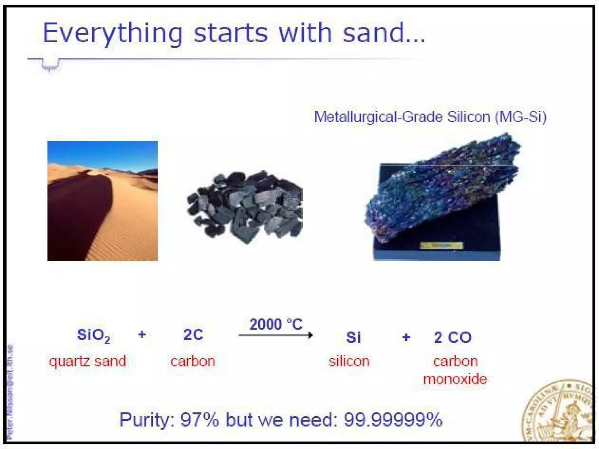
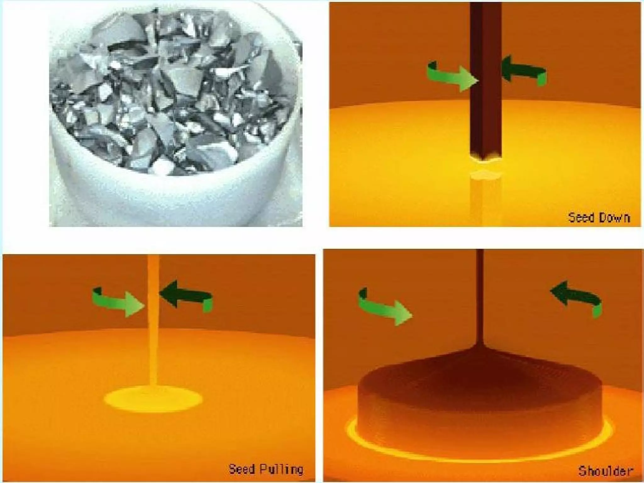
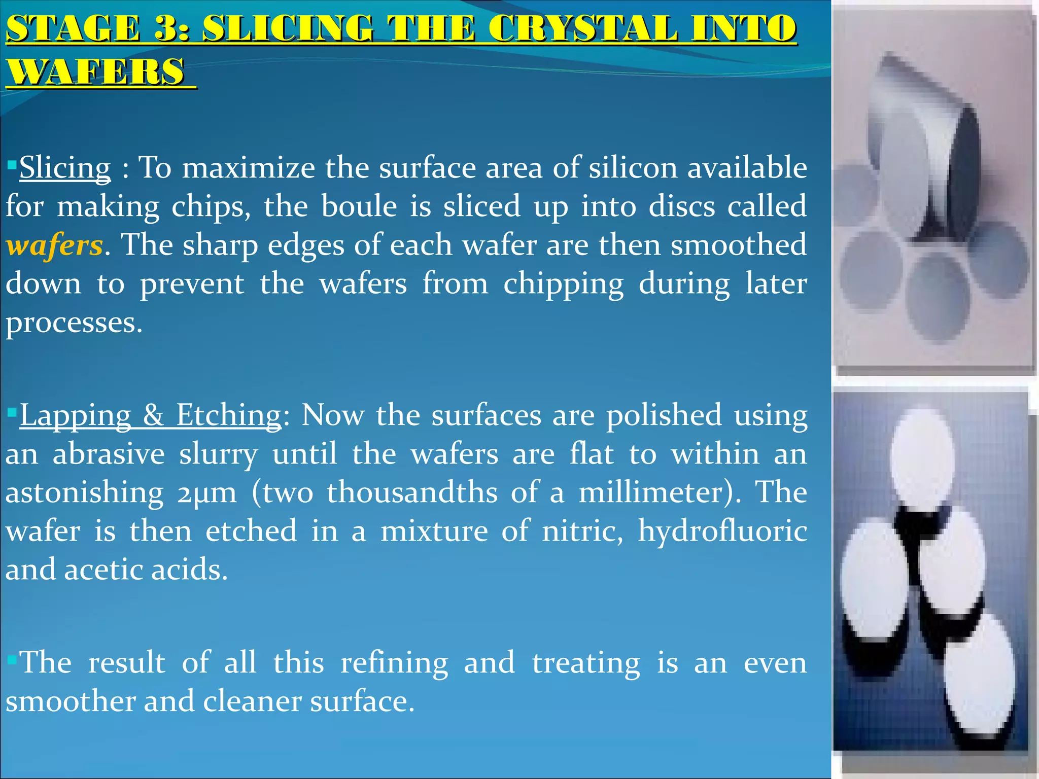
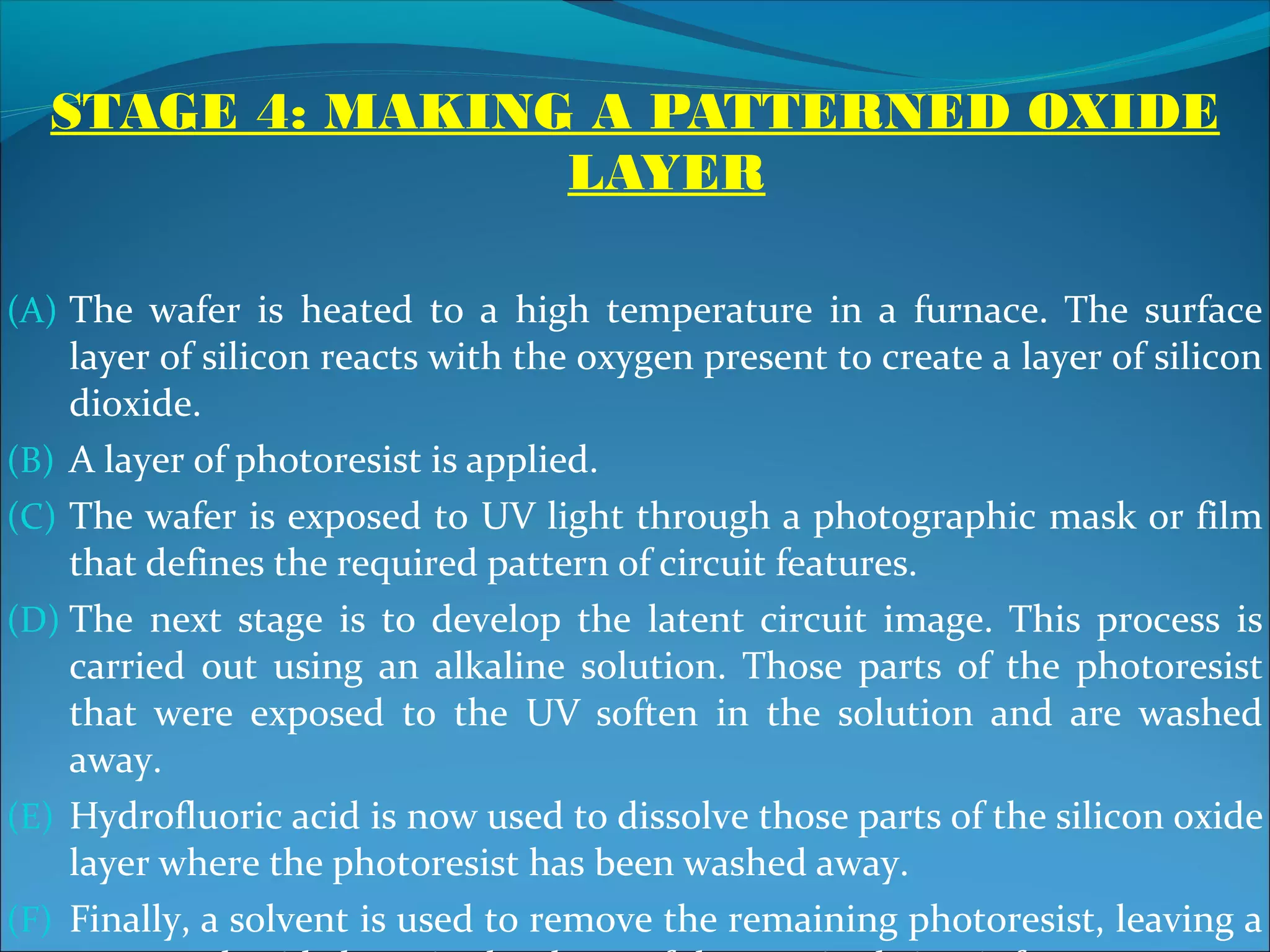
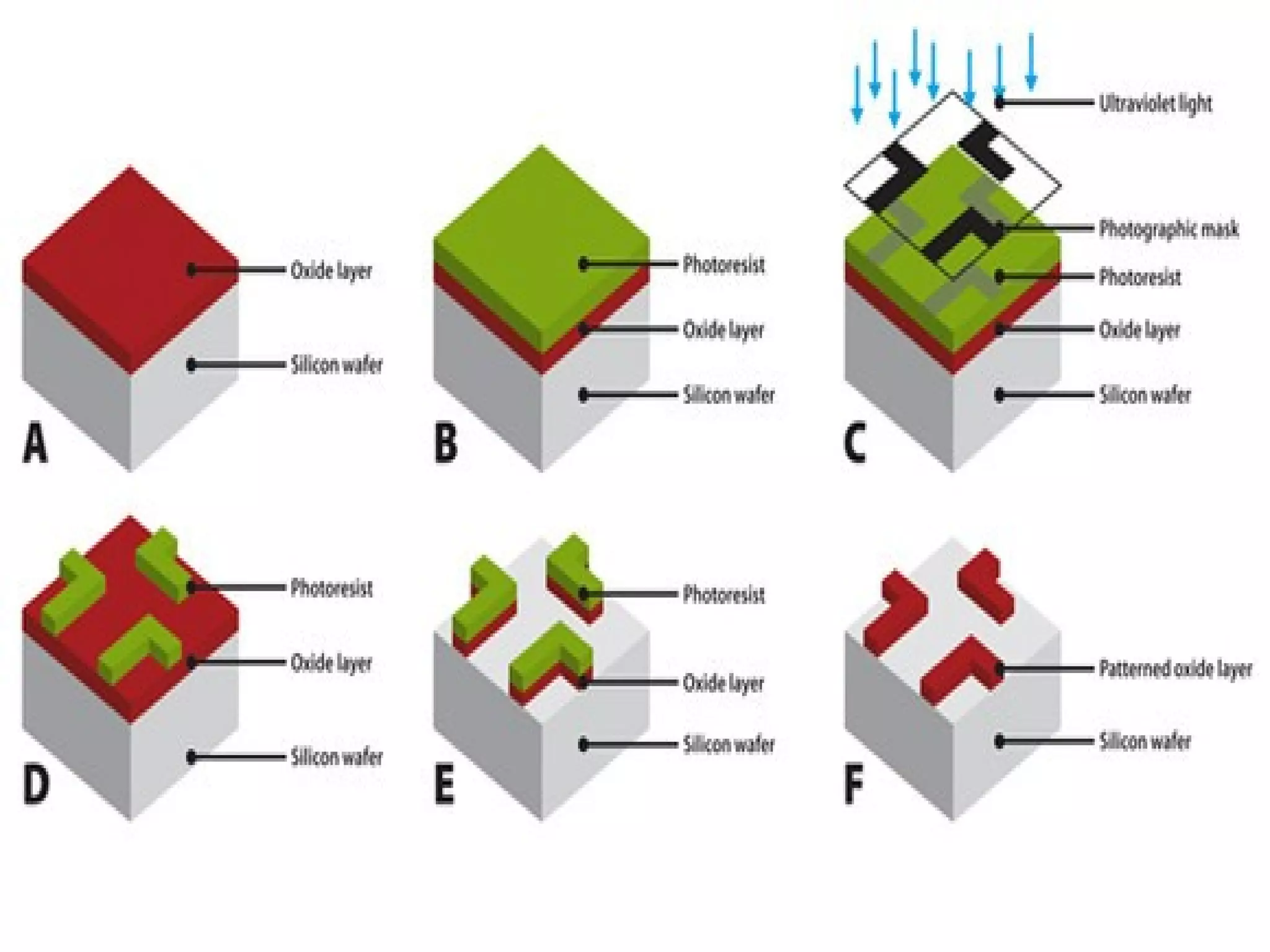
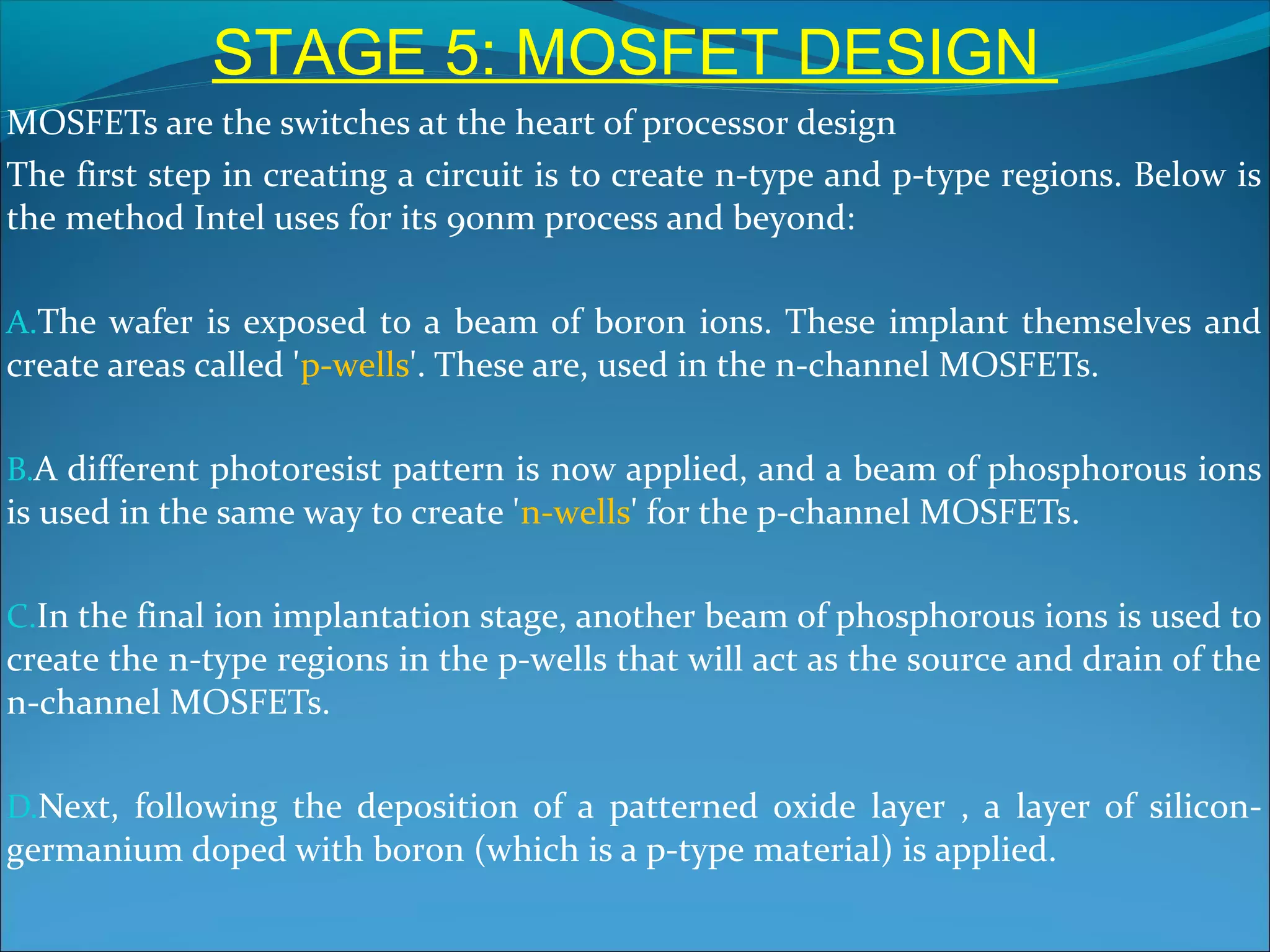
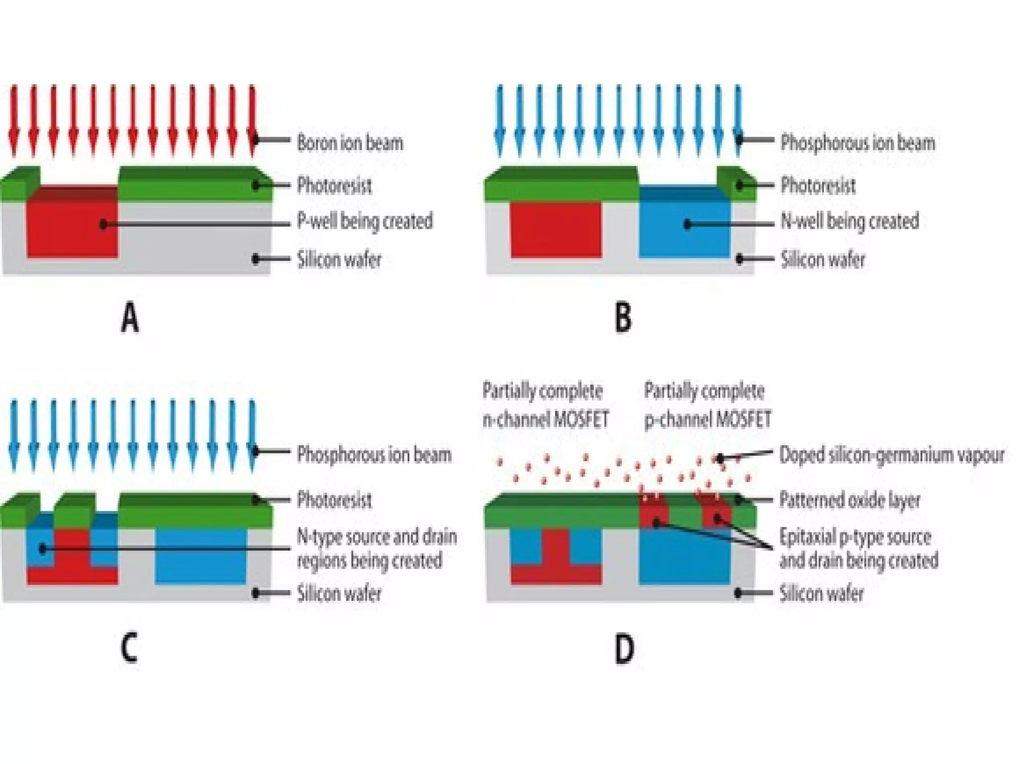
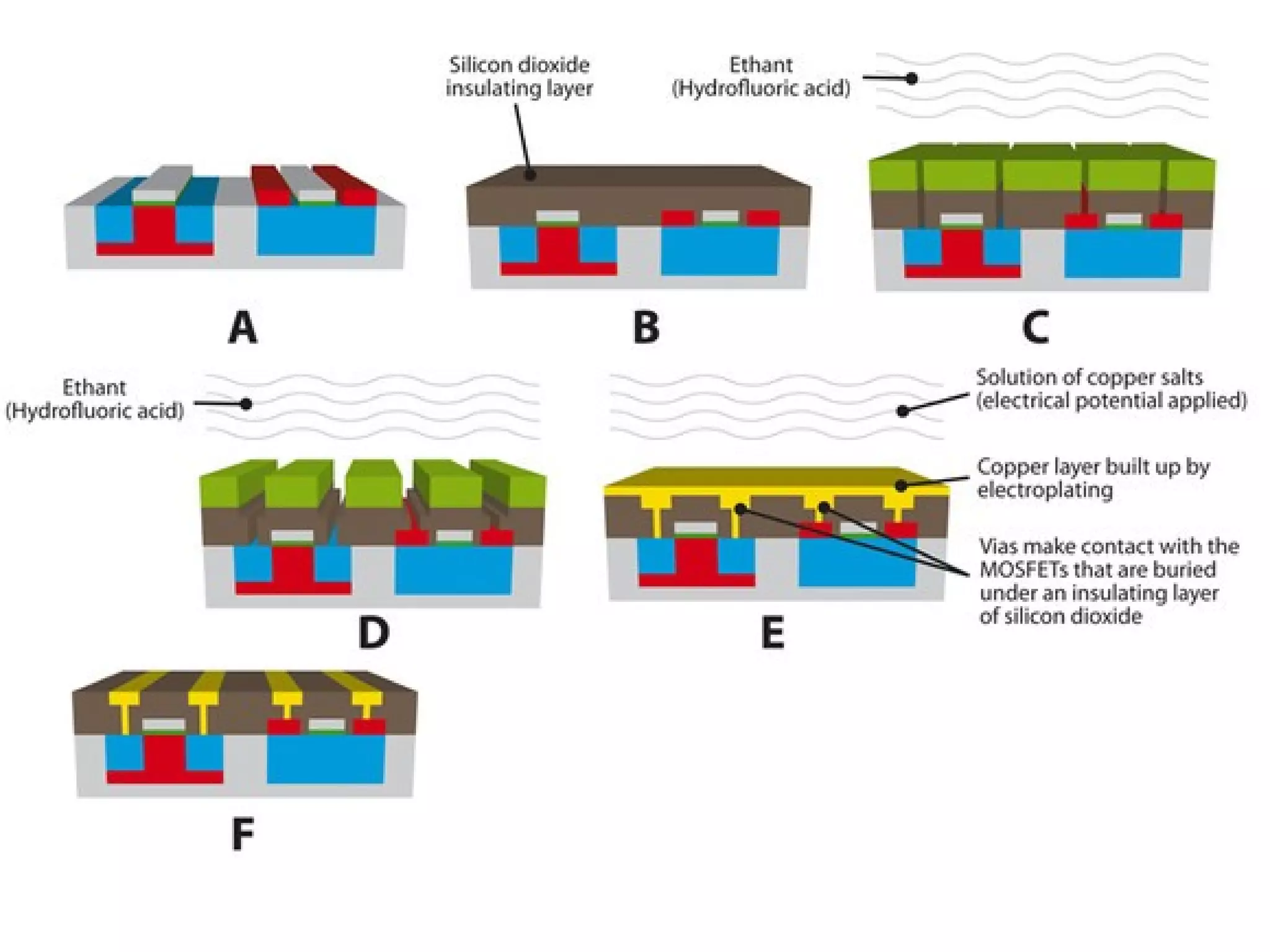
How sand is transformed into silicon
chips:
The amazing journey from sandcastle to Core i7
                                        Presented by:
                 Processor             Surabhi Singh
• The deserts of Arizona are home to Intel's Fab 32, a $3billion factory
that's performing one of the most complicated electrical engineering feats
of our time.

•It's here that processors with components measuring just 45 millionths of
a millimeter across are manufactured, ready to be shipped out to
motherboard manufacturers all over the world.

•It may seem an impossible transformation, but these complex
components are made from nothing more glamorous than sand. Such a
transformative feat isn't simple. The production process requires more
than 300 individual steps.

•An in-depth look at Intel's manufacturing method and the whole process
summed up into 10 stages.
STAGE 1:CONVERTING SAND TO
SILICON
• Sand is composed of silica (also known as silicon dioxide), and is the
starting point for making a processor.

•To extract the element silicon from the silica, it must be reduced. This is
accomplished by heating a mixture of silica and carbon in an electric arc
furnace to a temperature in excess of 2,000°C.

•The end result of this process is a substance referred to as metallurgical-
grade silicon, which is up to 97 percent pure.
Refinement: The silicon is ground to a fine powder and reacted with
gaseous hydrogen chloride in a fluidized bed reactor at 300°C to give a
liquid compound of silicon called trichlorosilane.


Impurities such as iron, aluminium, boron and phosphorous also react to
give their chlorides, which are then removed by fractional distillation. The
purified trichlorosilane is vaporized and reacted with hydrogen gas at
1,100°C so that the elemental silicon is retrieved.


During the reaction, silicon is deposited on the surface of an electrically
heated ultra-pure silicon rod to produce a silicon ingot. The end result is
referred to as electronic-grade silicon, and has a purity of 99.999999 per
cent.
STAGE 2 : CREATING A CYLINDRICAL
CRYSTAL
 Although pure to a very high degree, raw electronic-grade silicon has a
polycrystalline structure.

To turn it into a usable material, the silicon must be turned into single
crystals that have a regular atomic structure. This transformation is
achieved through the Czochralski Process. Electronic-grade silicon is
melted in a rotating quartz crucible and held at just above its melting point
of 1,414°C.

A tiny crystal of silicon is then dipped into the molten silicon and slowly
withdrawn while being continuously rotated in the opposite direction to
the rotation of the crucible. The crystal acts as a seed, causing silicon from
the crucible to crystallize around it. This builds up a rod – called a boule –
STAGE 3: SLICING THE CRYSTAL INTO
WAFERS

Slicing : To maximize the surface area of silicon available
for making chips, the boule is sliced up into discs called
wafers. The sharp edges of each wafer are then smoothed
down to prevent the wafers from chipping during later
processes.

Lapping & Etching: Now the surfaces are polished using
an abrasive slurry until the wafers are flat to within an
astonishing 2μm (two thousandths of a millimeter). The
wafer is then etched in a mixture of nitric, hydrofluoric
and acetic acids.

The result of all this refining and treating is an even
smoother and cleaner surface.
STAGE 4: MAKING A PATTERNED OXIDE
                 LAYER

(A) The wafer is heated to a high temperature in a furnace. The surface
    layer of silicon reacts with the oxygen present to create a layer of silicon
    dioxide.
(B) A layer of photoresist is applied.
(C) The wafer is exposed to UV light through a photographic mask or film
    that defines the required pattern of circuit features.
(D) The next stage is to develop the latent circuit image. This process is
    carried out using an alkaline solution. Those parts of the photoresist
    that were exposed to the UV soften in the solution and are washed
    away.
(E) Hydrofluoric acid is now used to dissolve those parts of the silicon oxide
    layer where the photoresist has been washed away.
(F) Finally, a solvent is used to remove the remaining photoresist, leaving a
STAGE 5: MOSFET DESIGN
MOSFETs are the switches at the heart of processor design
The first step in creating a circuit is to create n-type and p-type regions. Below is
the method Intel uses for its 90nm process and beyond:

A.The wafer is exposed to a beam of boron ions. These implant themselves and
create areas called 'p-wells'. These are, used in the n-channel MOSFETs.

B.A different photoresist pattern is now applied, and a beam of phosphorous ions
is used in the same way to create 'n-wells' for the p-channel MOSFETs.

C.In the final ion implantation stage, another beam of phosphorous ions is used to
create the n-type regions in the p-wells that will act as the source and drain of the
n-channel MOSFETs.

D.Next, following the deposition of a patterned oxide layer , a layer of silicon-
germanium doped with boron (which is a p-type material) is applied.
STAGE 6: ADDING GATES TO COMPLETE THE
                    MOSFETS

 The first job is to produce a patterned oxide layer as described in Step 4.
In this case, the oxide layer will have gaps only in the gate regions of the
MOSFETs.

 The first part of the gate is a very thin insulating layer of silicon dioxide,
deposited on the surface of the silicon between the source and the drain.
This is done Using Chemical Vapor Deposition (CVD), a process that
takes place in a furnace filled with various gases that cause a chemical
reaction to take place on the surface of the silicon.

 To complete the MOSFET, a layer of silicon is applied over the top of the
thin oxide layer to act as a conductor. Again, CVD is used, and the silicon
is applied via an oxidation reaction.
STAGE 7: CONNECTING THE MOSFETS WITH
                  COPPER TRACKS

Once all of this has been done, the wafer will contain billions of MOSFETs. In order for
them to work together as circuits, they need to be connected together to produce lots of
individual chips, each of them still containing millions of MOSFETs. The process used by
Intel is as follows:


A.The initial state of the MOSFETs on the wafer.
B.A layer of insulation (silicon dioxide) has to be applied to the wafer so that the
interconnecting tracks don't short all the MOSFETs.
C.Hydrofluoric acid is used to etch holes in the silicon dioxide insulation.
D.After that, trenches in the pattern of the required interconnection tracks are
etched into the silicon dioxide through another photoresist layer.
E.A top layer of copper is then applied by electroplating. The resultant metallic
pins that protrude through the insulating layer are called 'vias'.
F.The wafer is now covered in a layer of copper. The final stage is to take this off.
In a process called chemical-mechanical polishing, the excess copper is removed.
STAGE 8: COMPLETING THE CIRCUIT

 An insulating layer of silicon dioxide protects the MOSFETs. Holes
etched through it permit connections to be made.

It's not always feasible to wire up a circuit without wires crossing. If there
was just one rogue interconnection, any tracks that crossed would short.

To avoid this, MOSFETs have more than one metallic layer, each
insulated by another layer of silicon dioxide and connected using vias.
STAGE 9: SORTING THE GOOD CHIPS FROM
                 THE BAD

 All being well, the wafer should now contain a couple of hundred dies
(the official name for chips), but in reality, not all of them will work
correctly.

The next job is therefore to find out which dies are working, a task that is
carried out by a wafer probe. This piece of hardware uses pins that line up
with the contacts on a die, through which electrical signals can be passed to
put the processor through its paces.

 Dies are categorized as 'functional' or 'non-functional', but there might
also be several examples of partially functional dies.

Processors in which only some of the dies are working can still be sold as a
STAGE 10 : PACKAGING TO SURVIVE THE REAL
                      WORLD

We might have a fully working die now, but, as it stands, it's much too
fragile to ship to a motherboard manufacturer. Furthermore, the die has
hundreds or thousands of connections to the outside world, but it's only a few
millimeters square, making it far too fiddly for an electronics company to
make connectors for it.

The final step, therefore, is to encase the bare chip into a package that
most people would think of as a 'processor. The end result is that the die is
firmly attached to the package, and electrical connections are made between
the contacts on the die and the contacts on the package.

A final test on the finished assembly is all that's needed before the processor
can be shipped to a manufacturer and ultimately used to power a computer.
Liquid Metal Makes Silicon Crystals at Record Low
                      Temperatures
Jan. 24, 2013 — A new way of making crystalline silicon, developed by U-M
researchers, could make this crucial ingredient of computers and solar cells much
cheaper and greener.
Silicon dioxide, or sand, makes up about 40 percent of Earth's crust, but the industrial
method for converting sand into crystalline silicon is expensive and has a major
environmental impact due to the extreme processing conditions.
Recently, Maldonado and chemistry graduate students Junsi Gu and Eli Fahrenkrug
discovered a way to make silicon crystals directly at just 180 F. And they did it by
taking advantage of a phenomenon you can see right in your kitchen.
When water is super-saturated with sugar, that sugar can spontaneously form crystals,
popularly known as rock candy.
"Instead of water, we're using liquid metal, and instead of sugar, we're using silicon,"
Maldonado said.
Maldonado and colleagues made a solution containing silicon tetrachloride and layered
it over a liquid gallium electrode. Electrons from the metal converted the silicon
tetrachloride into raw silicon, which then dissolved into the liquid metal.
"The liquid metal is the key aspect of our process," Maldonado said. "Many solid metals
can also deliver electrons that transform silicon tetrachloride into disordered silicon, but
only metals like gallium can additionally serve as liquids for silicon crystallization
without additional heat."
The researchers reported dark films of silicon crystals accumulating on the
surfaces of their liquid gallium electrodes. So far, the crystals are very small,
about 1/2000th of a millimeter in diameter, but Maldonado hopes to improve the
technique and make larger silicon crystals, tailored for applications such as
converting light energy to electricity or storing energy. The team is exploring
several variations on the process, including the use of other low-melting-point
metal alloys.
If the approach proves viable, the implications could be huge, especially for the
solar energy industry. Crystalline silicon is presently the most-used solar energy
material, but the cost of silicon has driven many researchers to actively seek
alternative semiconductors.
"It's too premature to estimate precisely how much the process could lower the
price of silicon, but the potential for a scalable, dramatically less expensive and
more environmentally benign process is there," Maldonado said. "The dream
ultimately is to go from sand to crystalline silicon in one step. There's no
fundamental law that says this can't be done."
The study, which appears in the Journal of the American Chemical Society, was
funded by the American Chemical Society Petroleum Research Fund.
The university is pursuing patent protection for the intellectual property and is
seeking commercialization partners to help bring the technology to market.
Making of a silicon chip

Making of a silicon chip

  • 1.
    How sand istransformed into silicon chips: The amazing journey from sandcastle to Core i7 Presented by: Processor Surabhi Singh
  • 2.
    • The desertsof Arizona are home to Intel's Fab 32, a $3billion factory that's performing one of the most complicated electrical engineering feats of our time. •It's here that processors with components measuring just 45 millionths of a millimeter across are manufactured, ready to be shipped out to motherboard manufacturers all over the world. •It may seem an impossible transformation, but these complex components are made from nothing more glamorous than sand. Such a transformative feat isn't simple. The production process requires more than 300 individual steps. •An in-depth look at Intel's manufacturing method and the whole process summed up into 10 stages.
  • 3.
    STAGE 1:CONVERTING SANDTO SILICON • Sand is composed of silica (also known as silicon dioxide), and is the starting point for making a processor. •To extract the element silicon from the silica, it must be reduced. This is accomplished by heating a mixture of silica and carbon in an electric arc furnace to a temperature in excess of 2,000°C. •The end result of this process is a substance referred to as metallurgical- grade silicon, which is up to 97 percent pure.
  • 5.
    Refinement: The siliconis ground to a fine powder and reacted with gaseous hydrogen chloride in a fluidized bed reactor at 300°C to give a liquid compound of silicon called trichlorosilane. Impurities such as iron, aluminium, boron and phosphorous also react to give their chlorides, which are then removed by fractional distillation. The purified trichlorosilane is vaporized and reacted with hydrogen gas at 1,100°C so that the elemental silicon is retrieved. During the reaction, silicon is deposited on the surface of an electrically heated ultra-pure silicon rod to produce a silicon ingot. The end result is referred to as electronic-grade silicon, and has a purity of 99.999999 per cent.
  • 6.
    STAGE 2 :CREATING A CYLINDRICAL CRYSTAL  Although pure to a very high degree, raw electronic-grade silicon has a polycrystalline structure. To turn it into a usable material, the silicon must be turned into single crystals that have a regular atomic structure. This transformation is achieved through the Czochralski Process. Electronic-grade silicon is melted in a rotating quartz crucible and held at just above its melting point of 1,414°C. A tiny crystal of silicon is then dipped into the molten silicon and slowly withdrawn while being continuously rotated in the opposite direction to the rotation of the crucible. The crystal acts as a seed, causing silicon from the crucible to crystallize around it. This builds up a rod – called a boule –
  • 8.
    STAGE 3: SLICINGTHE CRYSTAL INTO WAFERS Slicing : To maximize the surface area of silicon available for making chips, the boule is sliced up into discs called wafers. The sharp edges of each wafer are then smoothed down to prevent the wafers from chipping during later processes. Lapping & Etching: Now the surfaces are polished using an abrasive slurry until the wafers are flat to within an astonishing 2μm (two thousandths of a millimeter). The wafer is then etched in a mixture of nitric, hydrofluoric and acetic acids. The result of all this refining and treating is an even smoother and cleaner surface.
  • 9.
    STAGE 4: MAKINGA PATTERNED OXIDE LAYER (A) The wafer is heated to a high temperature in a furnace. The surface layer of silicon reacts with the oxygen present to create a layer of silicon dioxide. (B) A layer of photoresist is applied. (C) The wafer is exposed to UV light through a photographic mask or film that defines the required pattern of circuit features. (D) The next stage is to develop the latent circuit image. This process is carried out using an alkaline solution. Those parts of the photoresist that were exposed to the UV soften in the solution and are washed away. (E) Hydrofluoric acid is now used to dissolve those parts of the silicon oxide layer where the photoresist has been washed away. (F) Finally, a solvent is used to remove the remaining photoresist, leaving a
  • 11.
    STAGE 5: MOSFETDESIGN MOSFETs are the switches at the heart of processor design The first step in creating a circuit is to create n-type and p-type regions. Below is the method Intel uses for its 90nm process and beyond: A.The wafer is exposed to a beam of boron ions. These implant themselves and create areas called 'p-wells'. These are, used in the n-channel MOSFETs. B.A different photoresist pattern is now applied, and a beam of phosphorous ions is used in the same way to create 'n-wells' for the p-channel MOSFETs. C.In the final ion implantation stage, another beam of phosphorous ions is used to create the n-type regions in the p-wells that will act as the source and drain of the n-channel MOSFETs. D.Next, following the deposition of a patterned oxide layer , a layer of silicon- germanium doped with boron (which is a p-type material) is applied.
  • 13.
    STAGE 6: ADDINGGATES TO COMPLETE THE MOSFETS  The first job is to produce a patterned oxide layer as described in Step 4. In this case, the oxide layer will have gaps only in the gate regions of the MOSFETs.  The first part of the gate is a very thin insulating layer of silicon dioxide, deposited on the surface of the silicon between the source and the drain. This is done Using Chemical Vapor Deposition (CVD), a process that takes place in a furnace filled with various gases that cause a chemical reaction to take place on the surface of the silicon.  To complete the MOSFET, a layer of silicon is applied over the top of the thin oxide layer to act as a conductor. Again, CVD is used, and the silicon is applied via an oxidation reaction.
  • 14.
    STAGE 7: CONNECTINGTHE MOSFETS WITH COPPER TRACKS Once all of this has been done, the wafer will contain billions of MOSFETs. In order for them to work together as circuits, they need to be connected together to produce lots of individual chips, each of them still containing millions of MOSFETs. The process used by Intel is as follows: A.The initial state of the MOSFETs on the wafer. B.A layer of insulation (silicon dioxide) has to be applied to the wafer so that the interconnecting tracks don't short all the MOSFETs. C.Hydrofluoric acid is used to etch holes in the silicon dioxide insulation. D.After that, trenches in the pattern of the required interconnection tracks are etched into the silicon dioxide through another photoresist layer. E.A top layer of copper is then applied by electroplating. The resultant metallic pins that protrude through the insulating layer are called 'vias'. F.The wafer is now covered in a layer of copper. The final stage is to take this off. In a process called chemical-mechanical polishing, the excess copper is removed.
  • 16.
    STAGE 8: COMPLETINGTHE CIRCUIT  An insulating layer of silicon dioxide protects the MOSFETs. Holes etched through it permit connections to be made. It's not always feasible to wire up a circuit without wires crossing. If there was just one rogue interconnection, any tracks that crossed would short. To avoid this, MOSFETs have more than one metallic layer, each insulated by another layer of silicon dioxide and connected using vias.
  • 17.
    STAGE 9: SORTINGTHE GOOD CHIPS FROM THE BAD  All being well, the wafer should now contain a couple of hundred dies (the official name for chips), but in reality, not all of them will work correctly. The next job is therefore to find out which dies are working, a task that is carried out by a wafer probe. This piece of hardware uses pins that line up with the contacts on a die, through which electrical signals can be passed to put the processor through its paces.  Dies are categorized as 'functional' or 'non-functional', but there might also be several examples of partially functional dies. Processors in which only some of the dies are working can still be sold as a
  • 18.
    STAGE 10 :PACKAGING TO SURVIVE THE REAL WORLD We might have a fully working die now, but, as it stands, it's much too fragile to ship to a motherboard manufacturer. Furthermore, the die has hundreds or thousands of connections to the outside world, but it's only a few millimeters square, making it far too fiddly for an electronics company to make connectors for it. The final step, therefore, is to encase the bare chip into a package that most people would think of as a 'processor. The end result is that the die is firmly attached to the package, and electrical connections are made between the contacts on the die and the contacts on the package. A final test on the finished assembly is all that's needed before the processor can be shipped to a manufacturer and ultimately used to power a computer.
  • 19.
    Liquid Metal MakesSilicon Crystals at Record Low Temperatures Jan. 24, 2013 — A new way of making crystalline silicon, developed by U-M researchers, could make this crucial ingredient of computers and solar cells much cheaper and greener. Silicon dioxide, or sand, makes up about 40 percent of Earth's crust, but the industrial method for converting sand into crystalline silicon is expensive and has a major environmental impact due to the extreme processing conditions. Recently, Maldonado and chemistry graduate students Junsi Gu and Eli Fahrenkrug discovered a way to make silicon crystals directly at just 180 F. And they did it by taking advantage of a phenomenon you can see right in your kitchen. When water is super-saturated with sugar, that sugar can spontaneously form crystals, popularly known as rock candy. "Instead of water, we're using liquid metal, and instead of sugar, we're using silicon," Maldonado said. Maldonado and colleagues made a solution containing silicon tetrachloride and layered it over a liquid gallium electrode. Electrons from the metal converted the silicon tetrachloride into raw silicon, which then dissolved into the liquid metal. "The liquid metal is the key aspect of our process," Maldonado said. "Many solid metals can also deliver electrons that transform silicon tetrachloride into disordered silicon, but only metals like gallium can additionally serve as liquids for silicon crystallization without additional heat."
  • 20.
    The researchers reporteddark films of silicon crystals accumulating on the surfaces of their liquid gallium electrodes. So far, the crystals are very small, about 1/2000th of a millimeter in diameter, but Maldonado hopes to improve the technique and make larger silicon crystals, tailored for applications such as converting light energy to electricity or storing energy. The team is exploring several variations on the process, including the use of other low-melting-point metal alloys. If the approach proves viable, the implications could be huge, especially for the solar energy industry. Crystalline silicon is presently the most-used solar energy material, but the cost of silicon has driven many researchers to actively seek alternative semiconductors. "It's too premature to estimate precisely how much the process could lower the price of silicon, but the potential for a scalable, dramatically less expensive and more environmentally benign process is there," Maldonado said. "The dream ultimately is to go from sand to crystalline silicon in one step. There's no fundamental law that says this can't be done." The study, which appears in the Journal of the American Chemical Society, was funded by the American Chemical Society Petroleum Research Fund. The university is pursuing patent protection for the intellectual property and is seeking commercialization partners to help bring the technology to market.