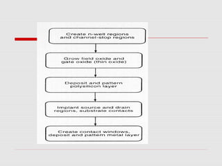
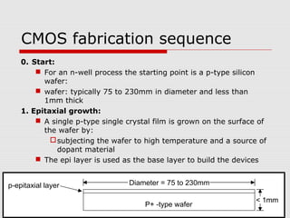
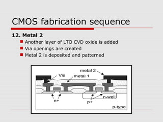
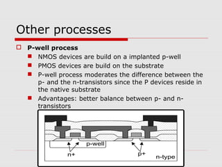
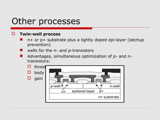
The document describes the key steps in CMOS fabrication:
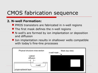
1. A p-type substrate is used, and n-well regions are defined through implantation to create isolation for p-MOSFETs.
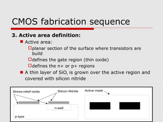
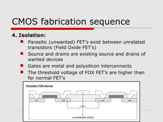
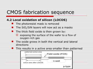
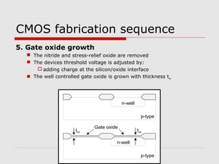
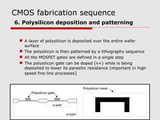
2. Active device regions and field oxide isolation are then patterned, followed by gate oxide growth and polysilicon deposition.
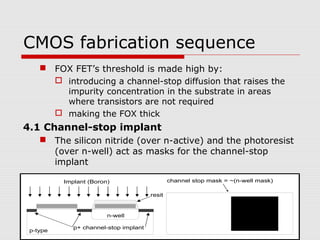
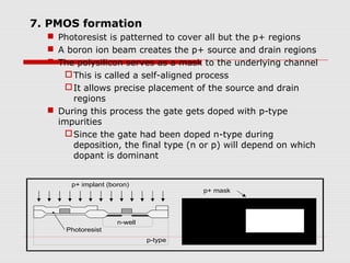
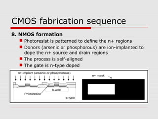
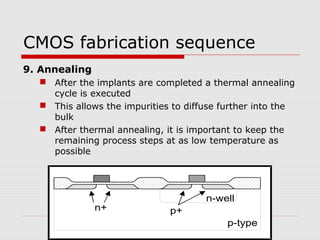
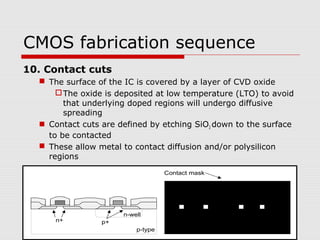
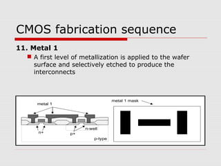
3. Self-aligned implantation creates n-type and p-type source/drain regions. Additional metallization layers connect the transistors.