Download as PDF, PPTX
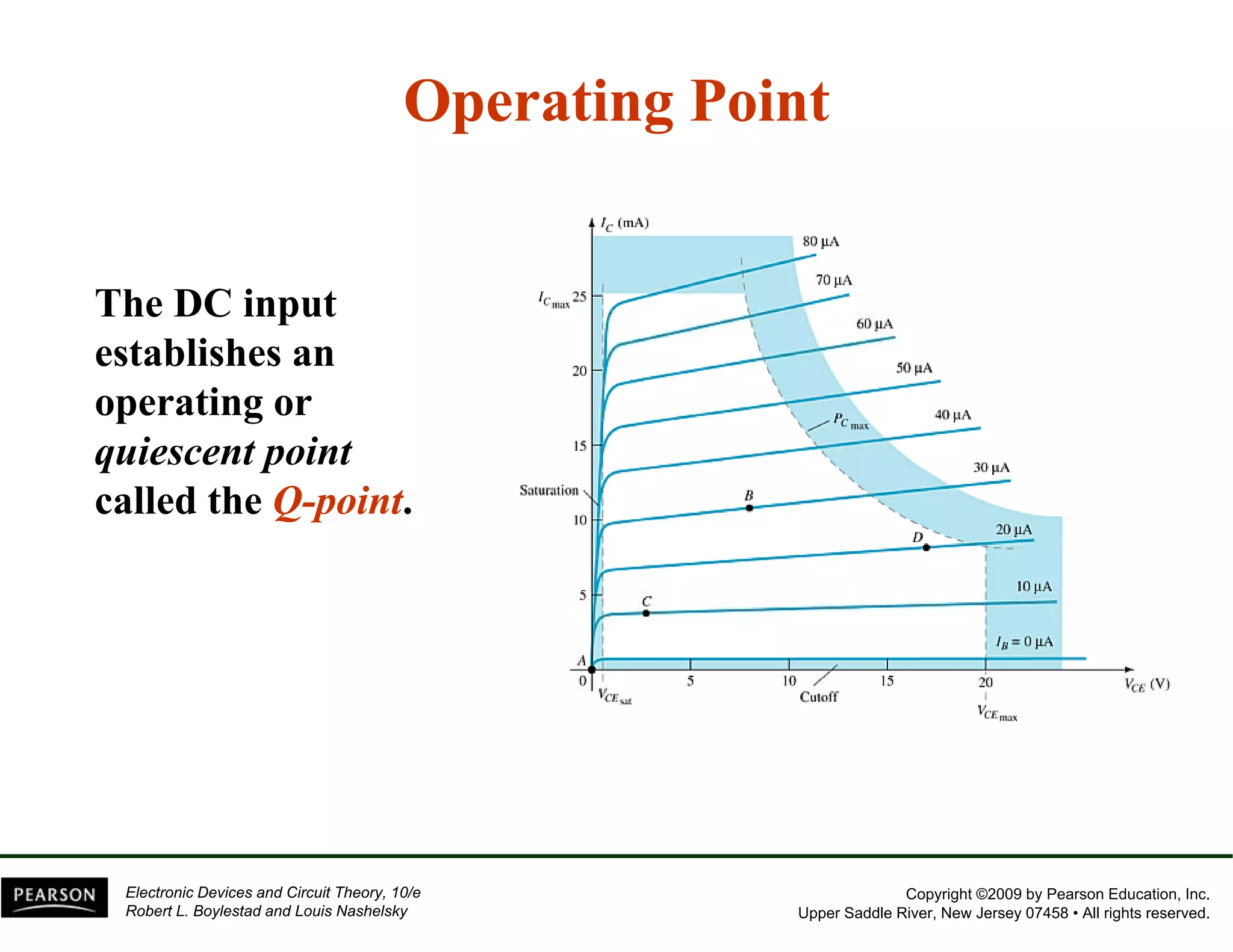
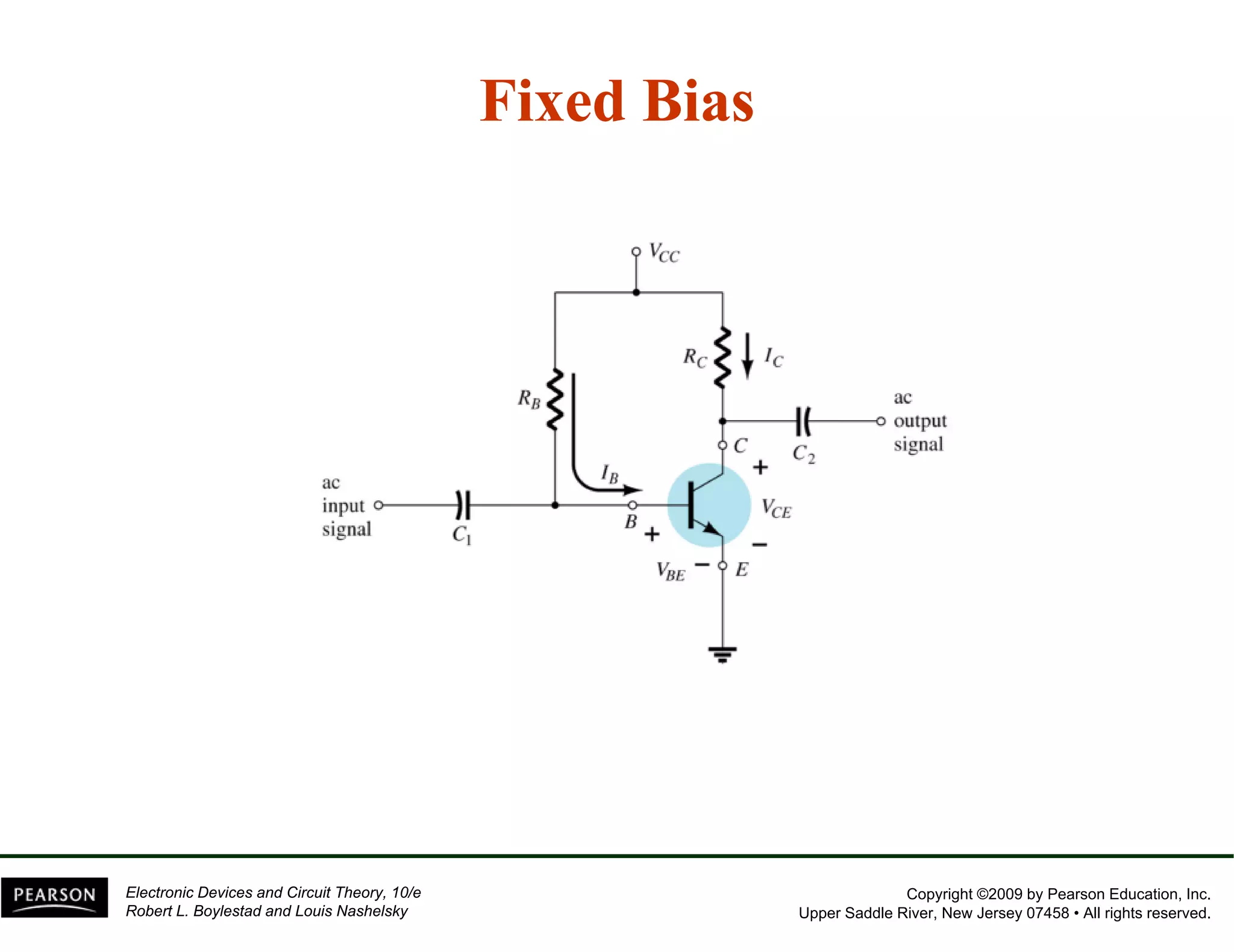
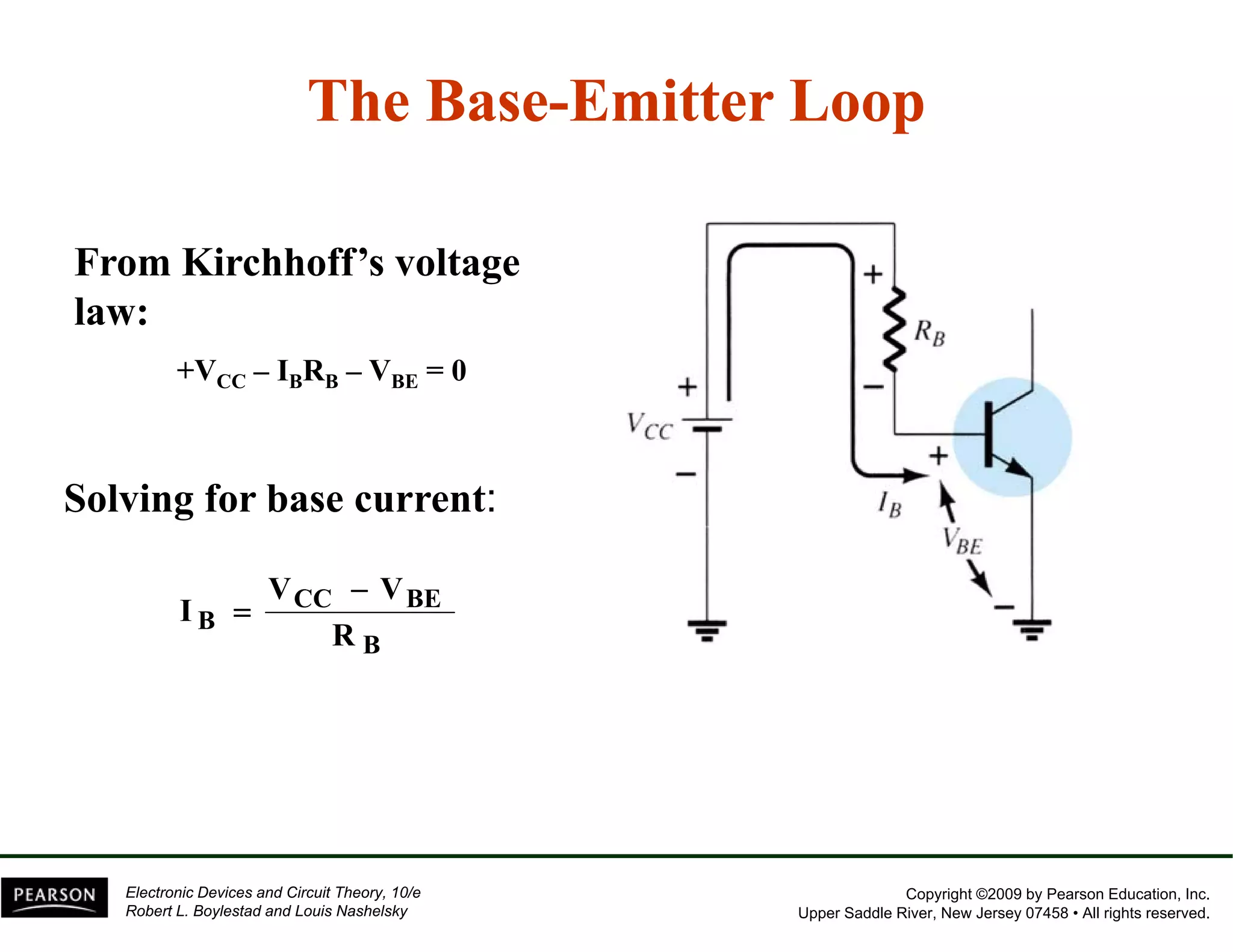
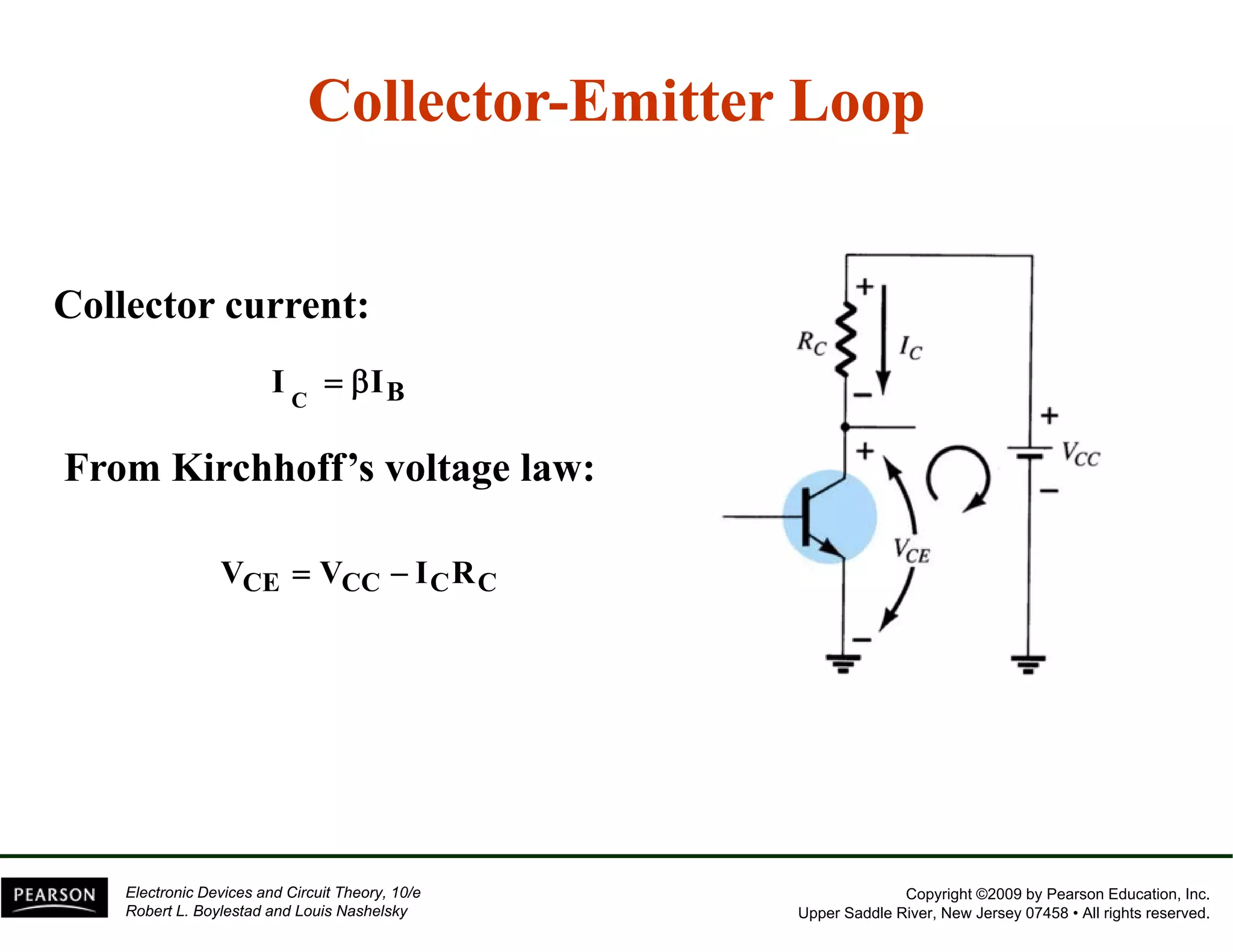
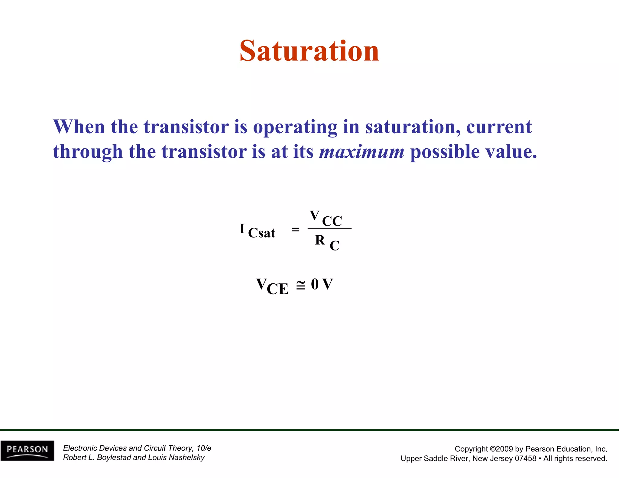
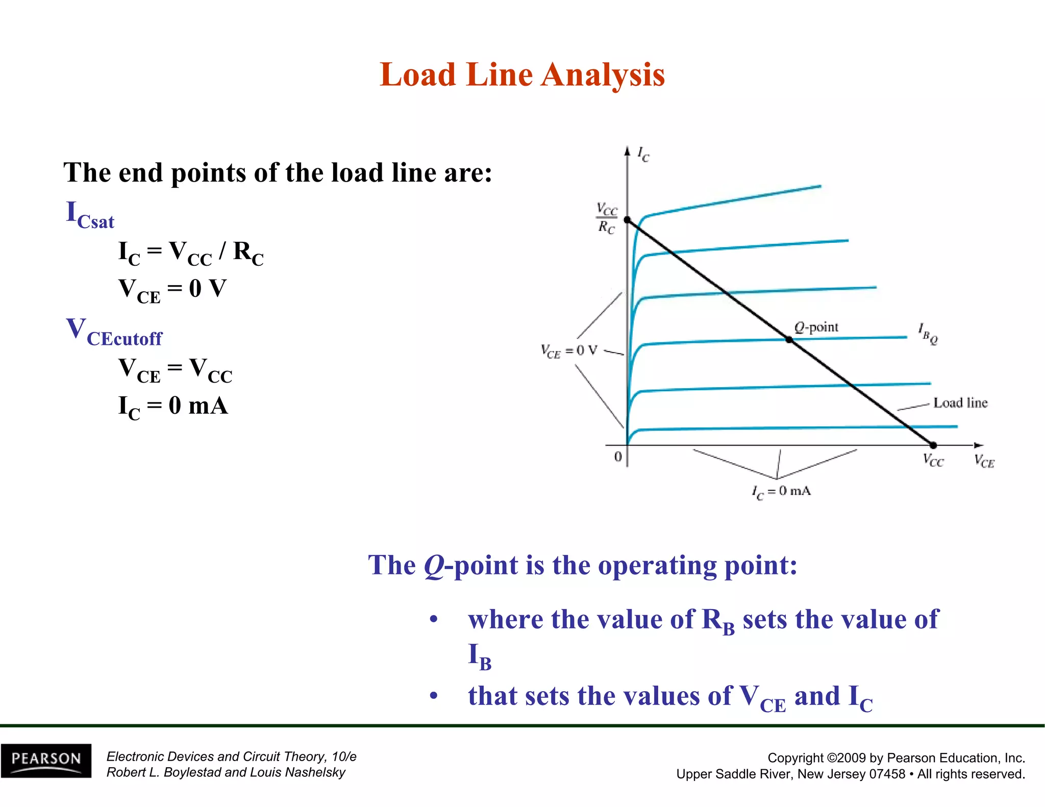
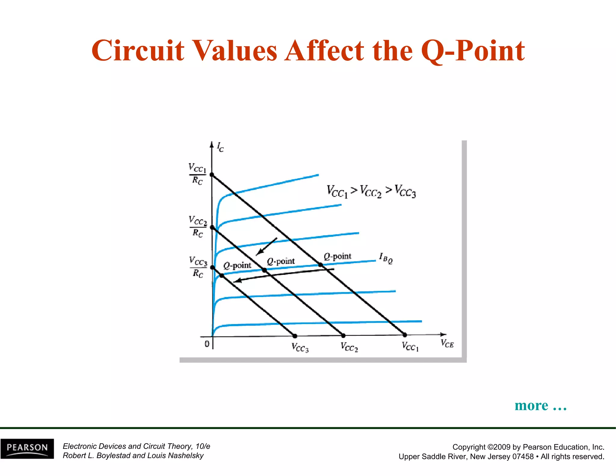
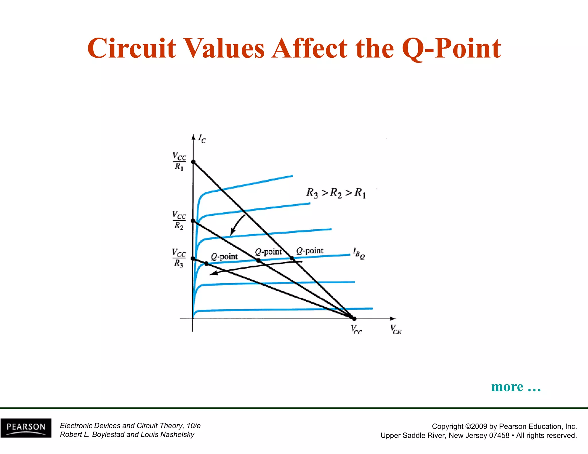
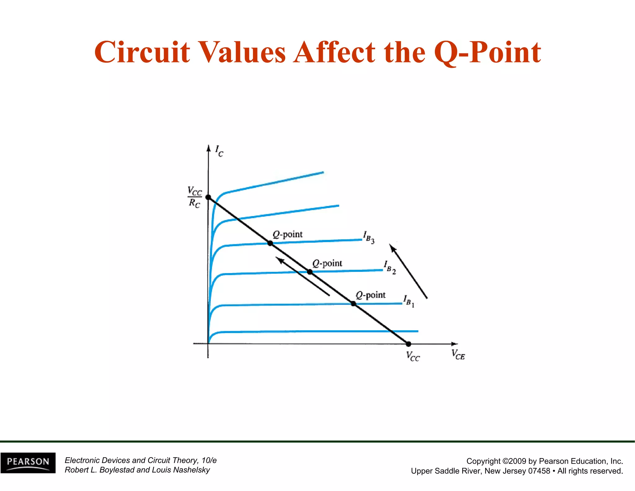
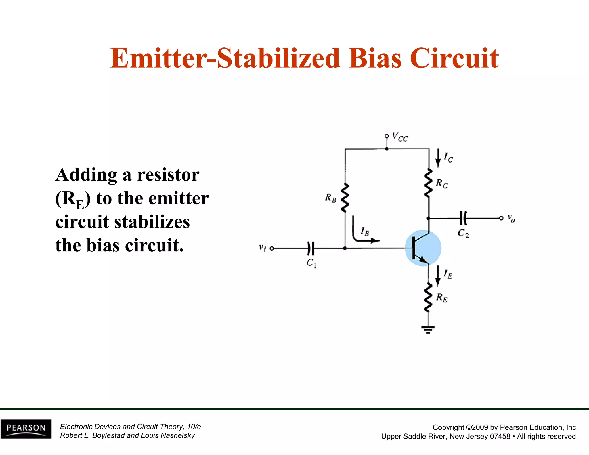
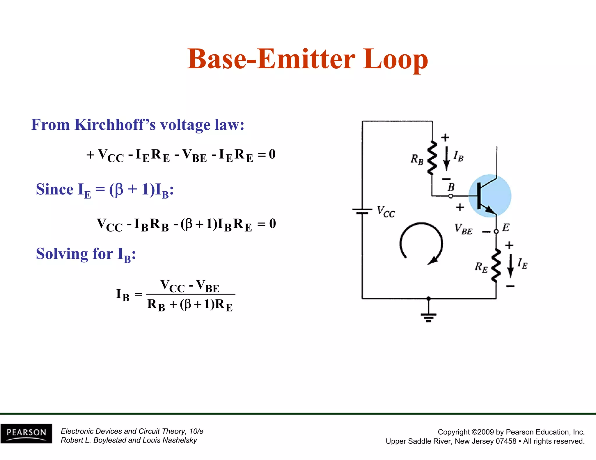
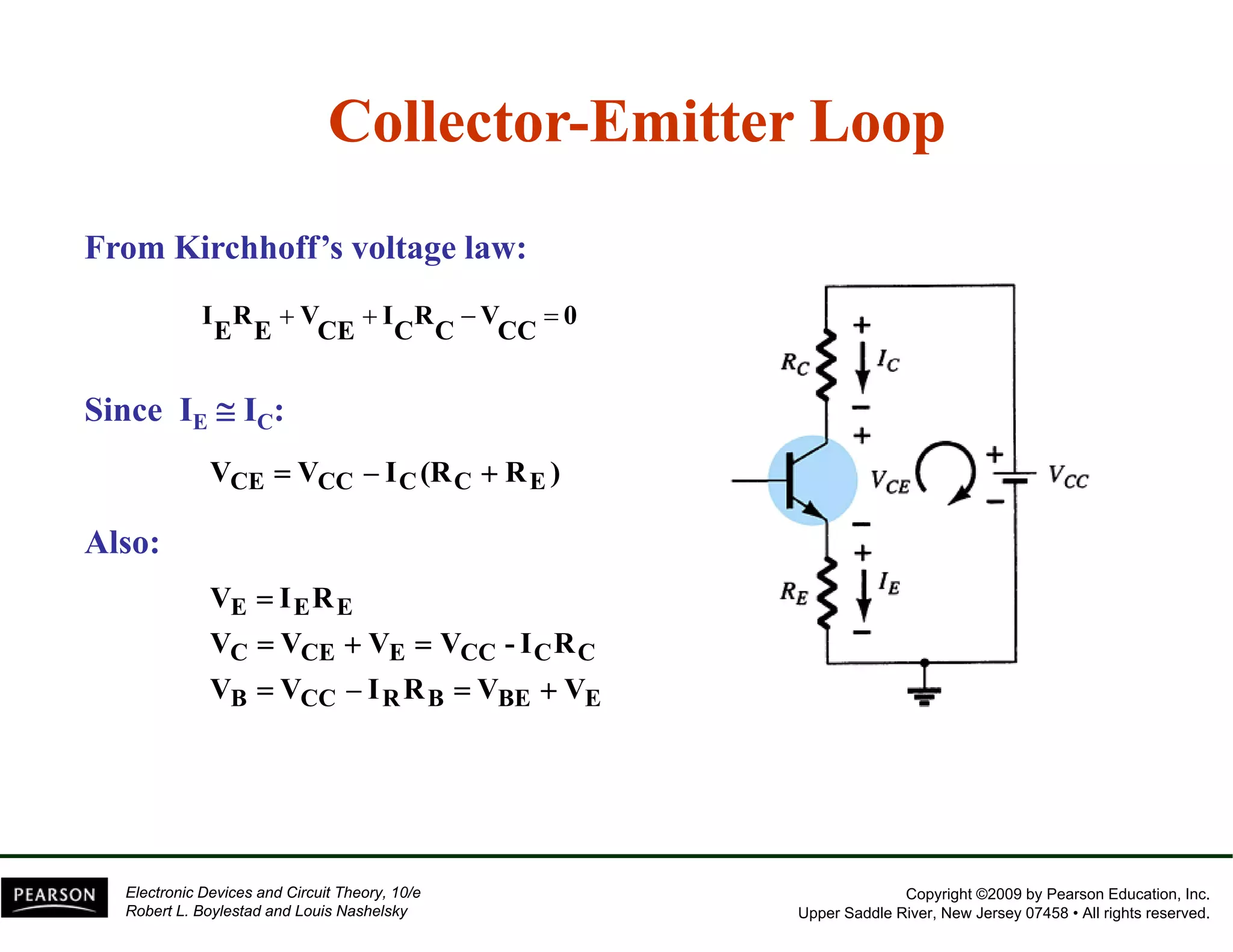
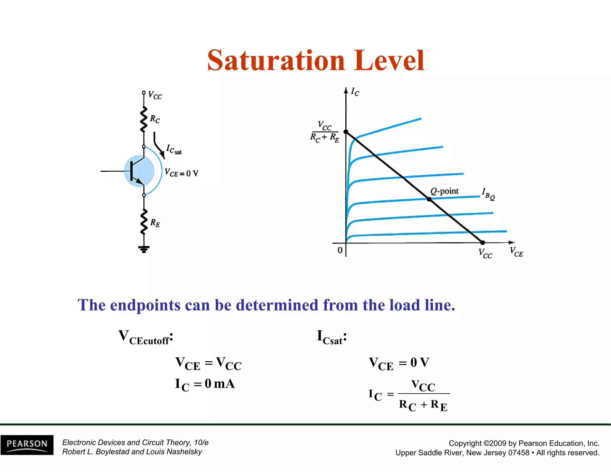
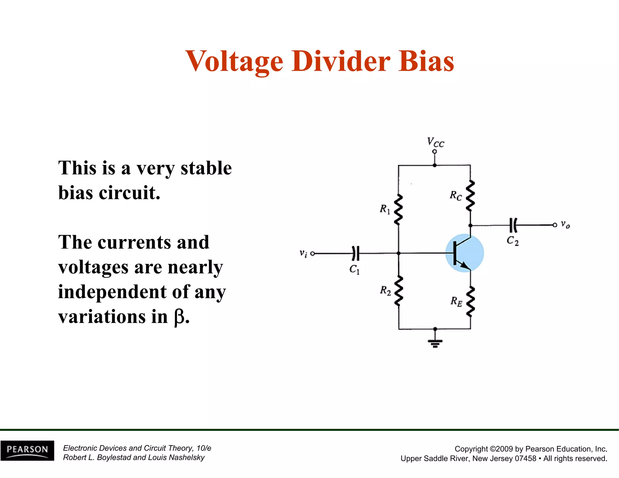
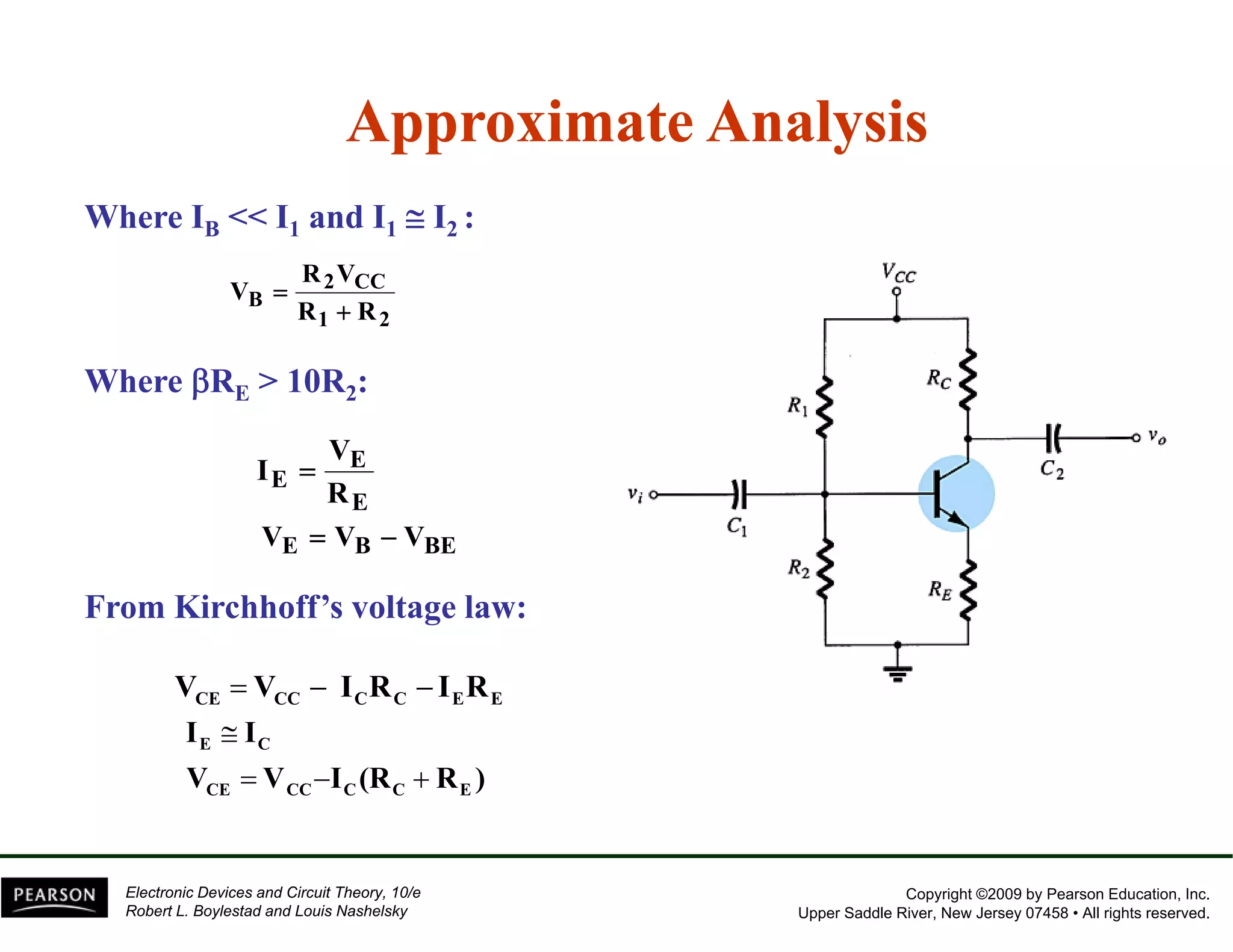
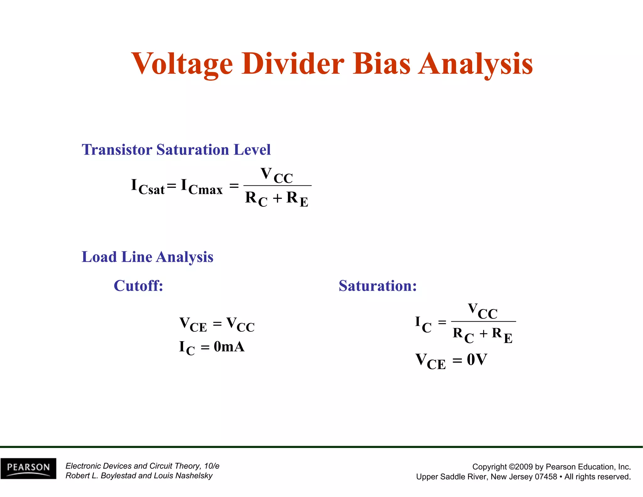
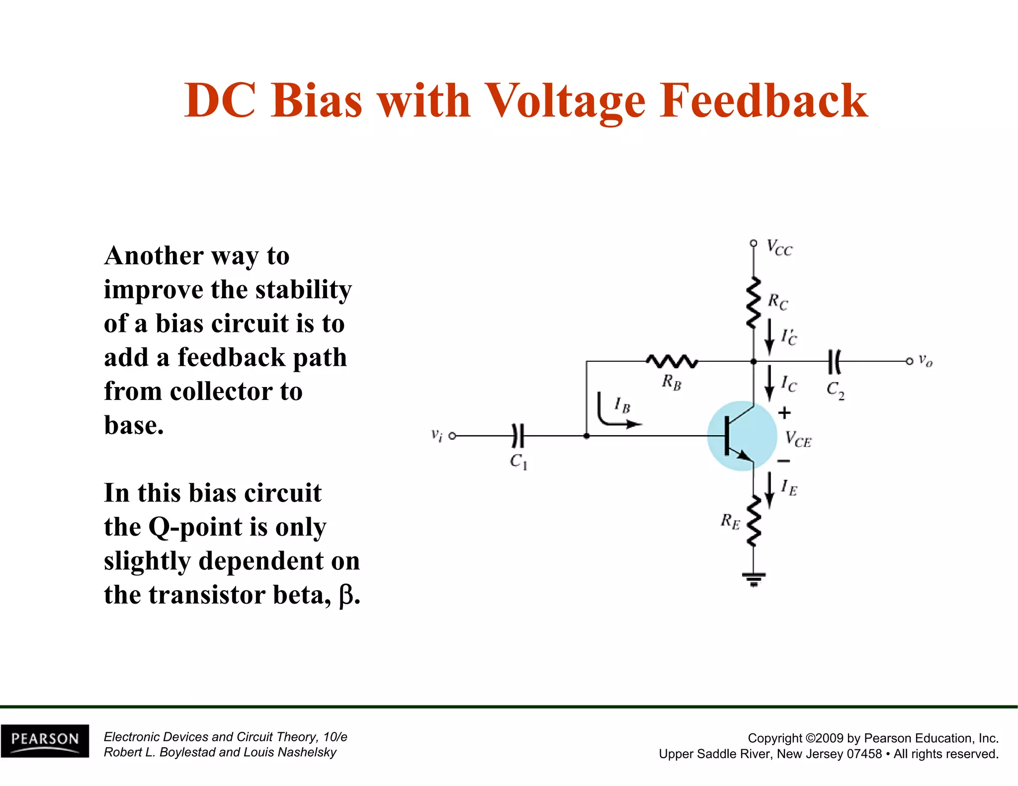
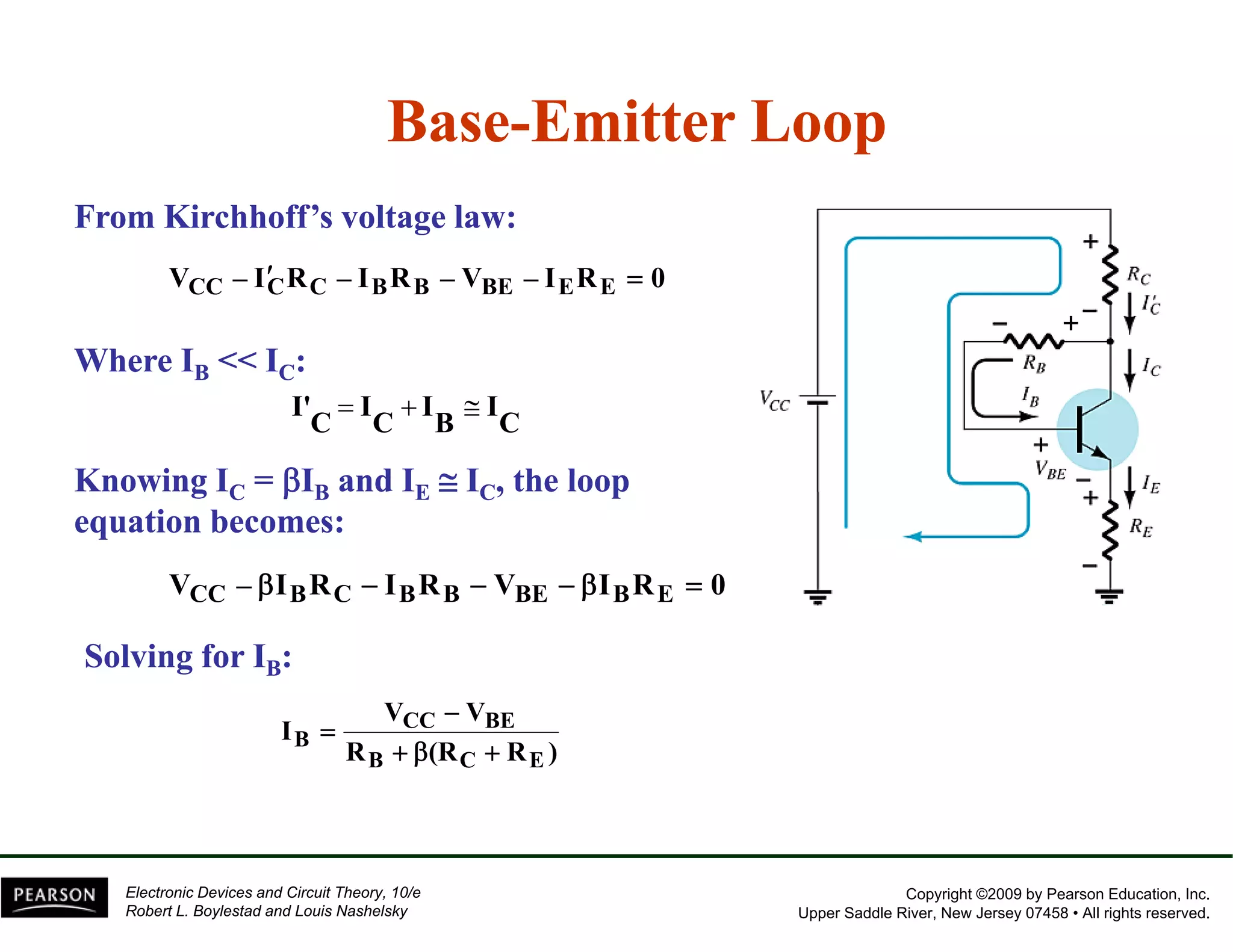
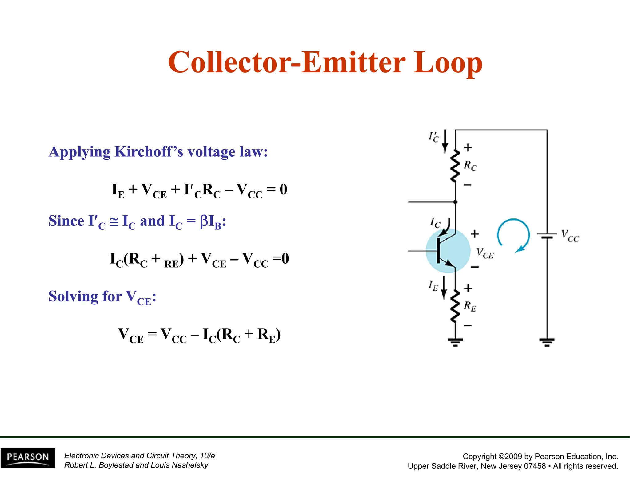
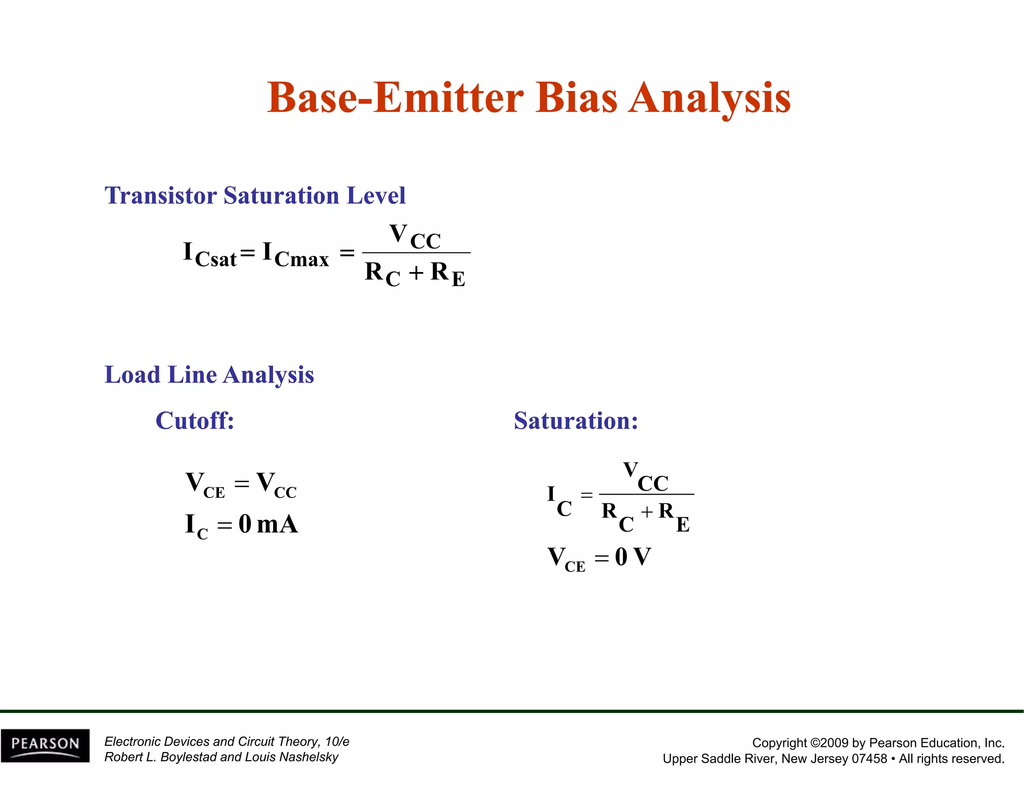
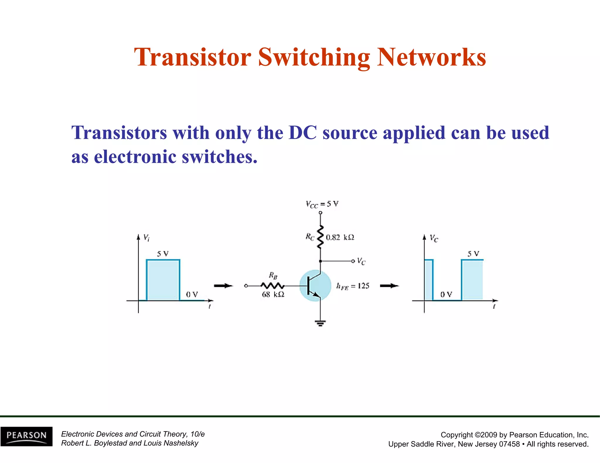
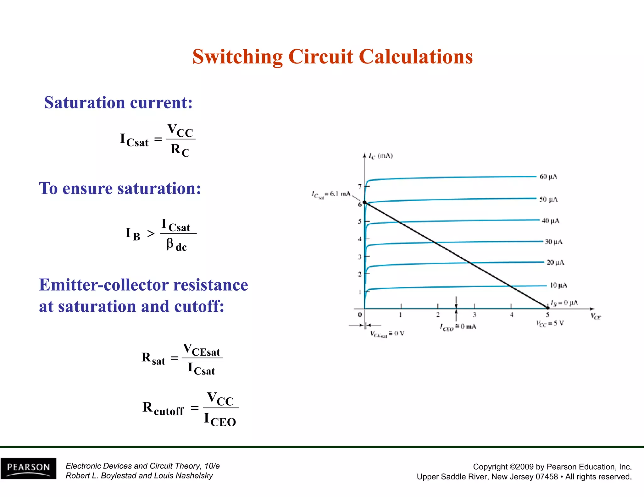
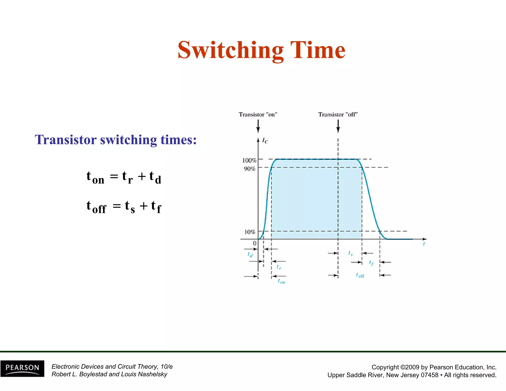

This document discusses different methods of biasing BJT transistors, including fixed bias, emitter-stabilized bias, and voltage divider bias circuits. It explains how the DC bias voltages establish an operating point (Q-point) for the transistor in either the active, cutoff, or saturation regions. Load line analysis is used to determine the transistor's Q-point based on the bias circuit components and supply voltage. Feedback circuits are also introduced to improve stability against variations in the transistor's beta value.


![RF Module Design - [Chapter 6] Power Amplifier](https://cdn.slidesharecdn.com/ss_thumbnails/rfch6-150613070347-lva1-app6891-thumbnail.jpg?width=640&height=640&fit=bounds)

![RF Circuit Design - [Ch2-2] Smith Chart](https://cdn.slidesharecdn.com/ss_thumbnails/ch2-2-150613064401-lva1-app6891-thumbnail.jpg?width=640&height=640&fit=bounds)


