Downloaded 137 times
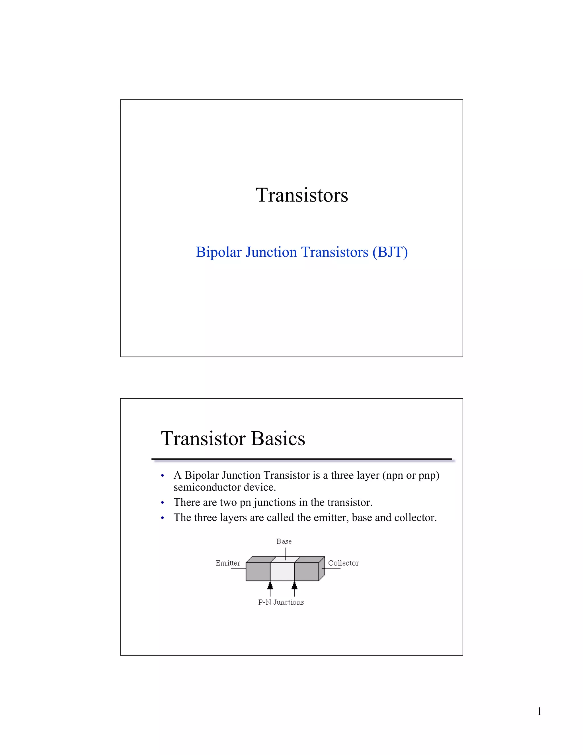
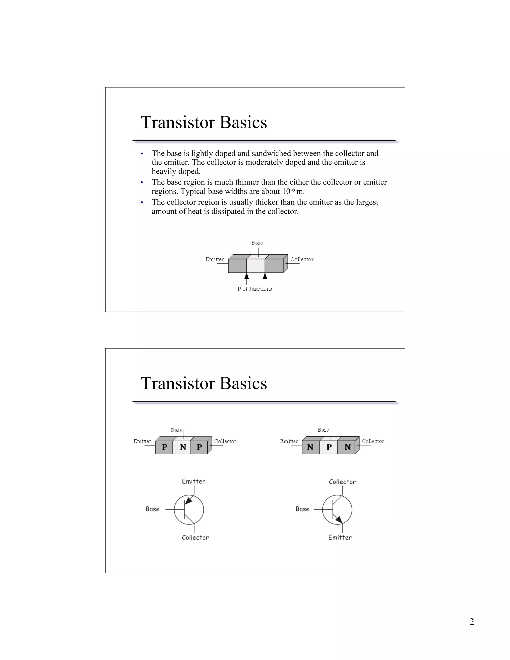

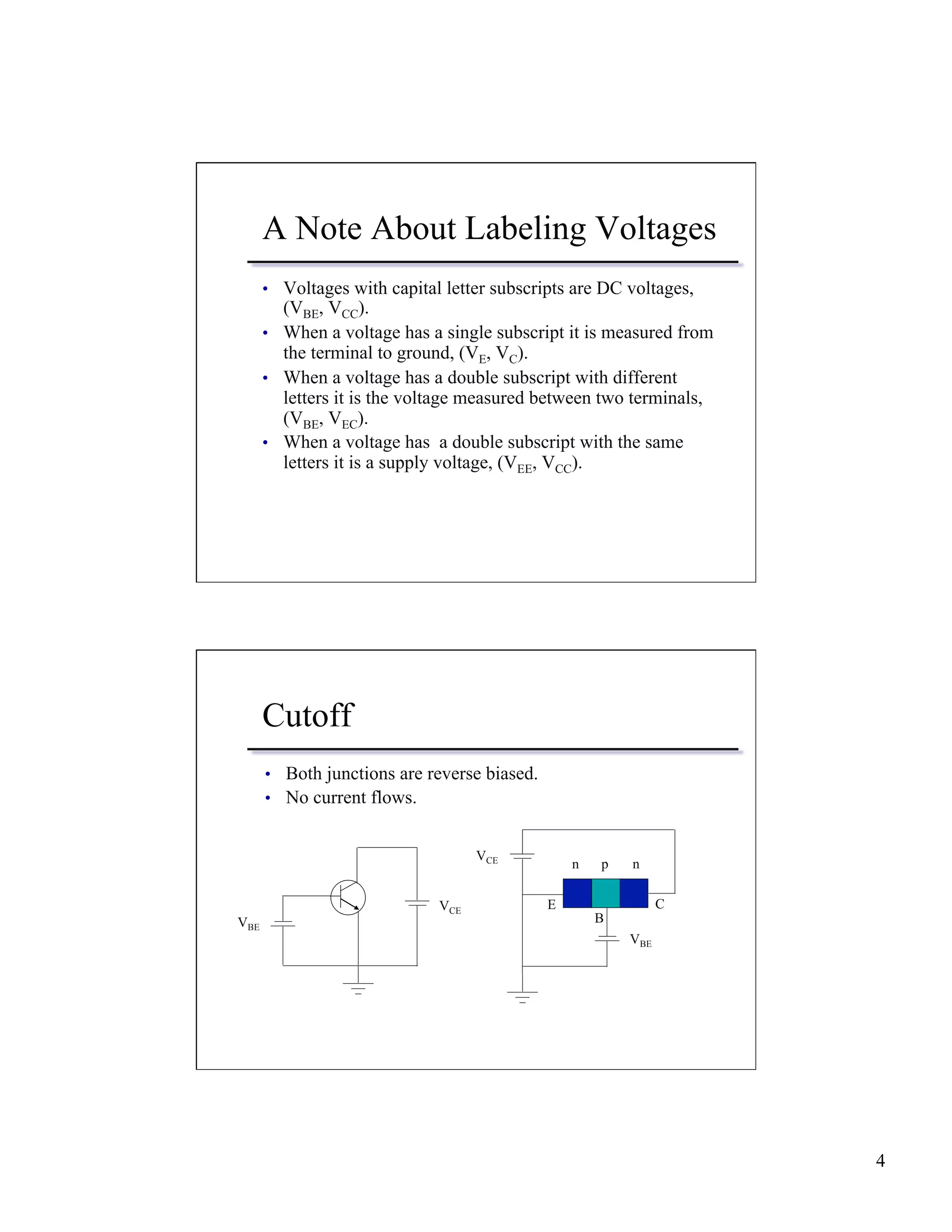
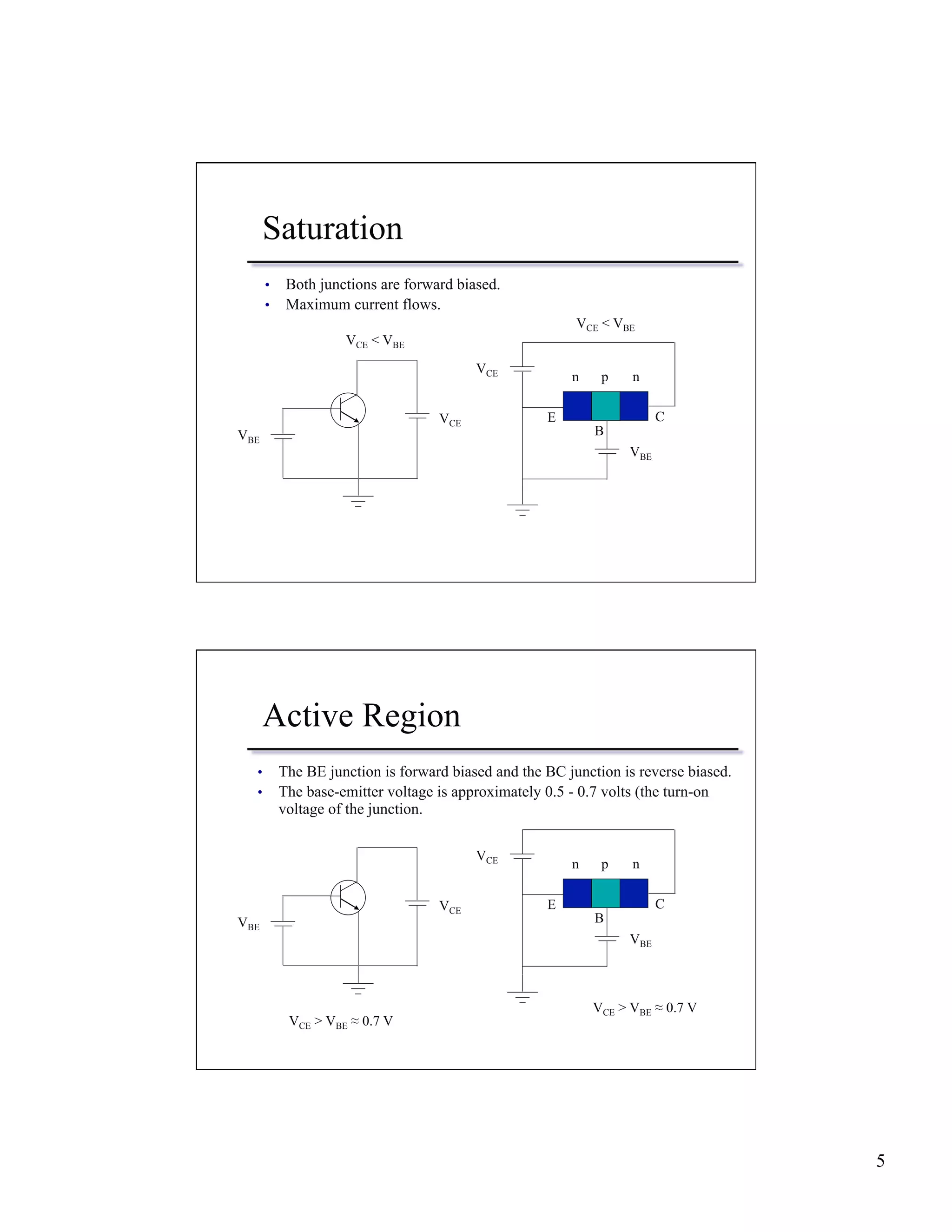
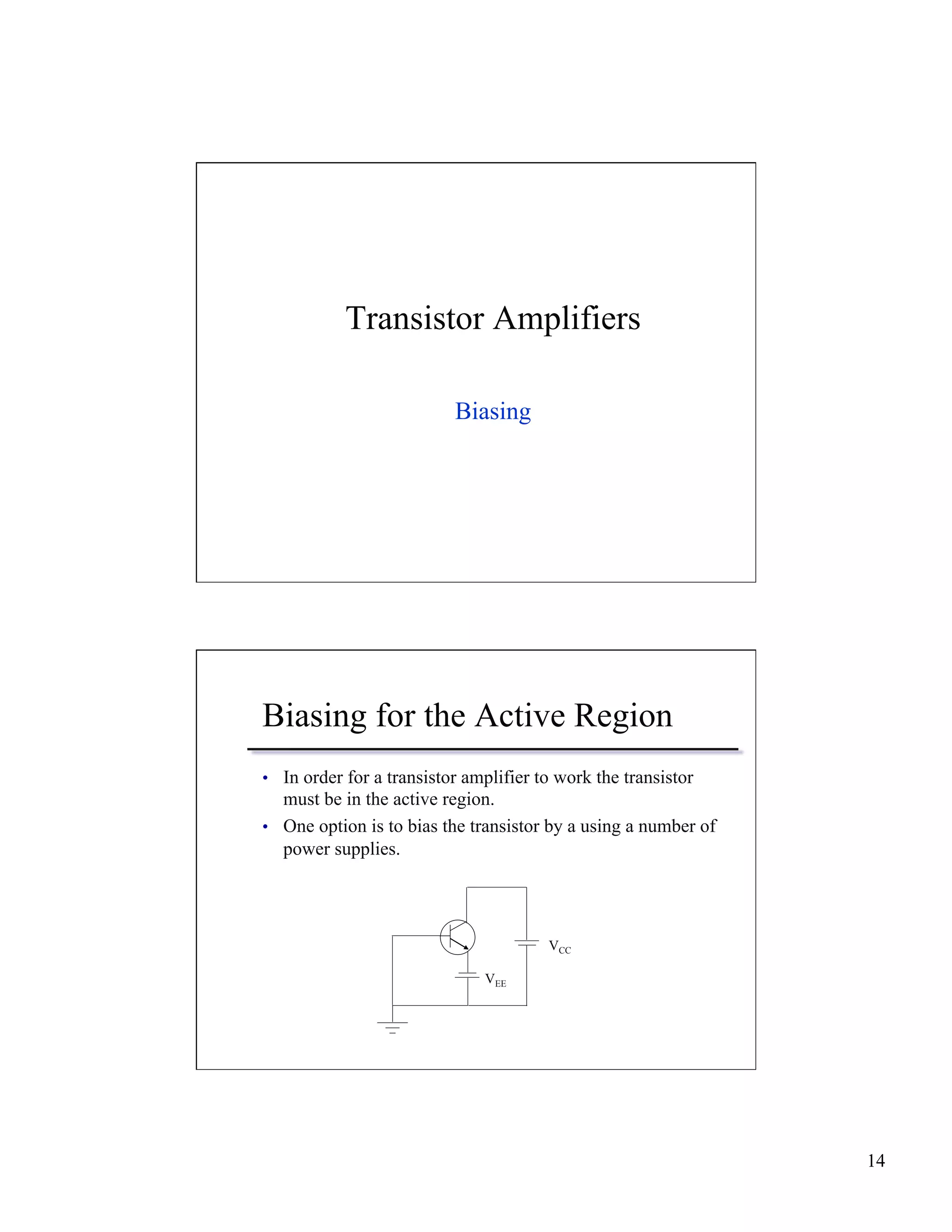
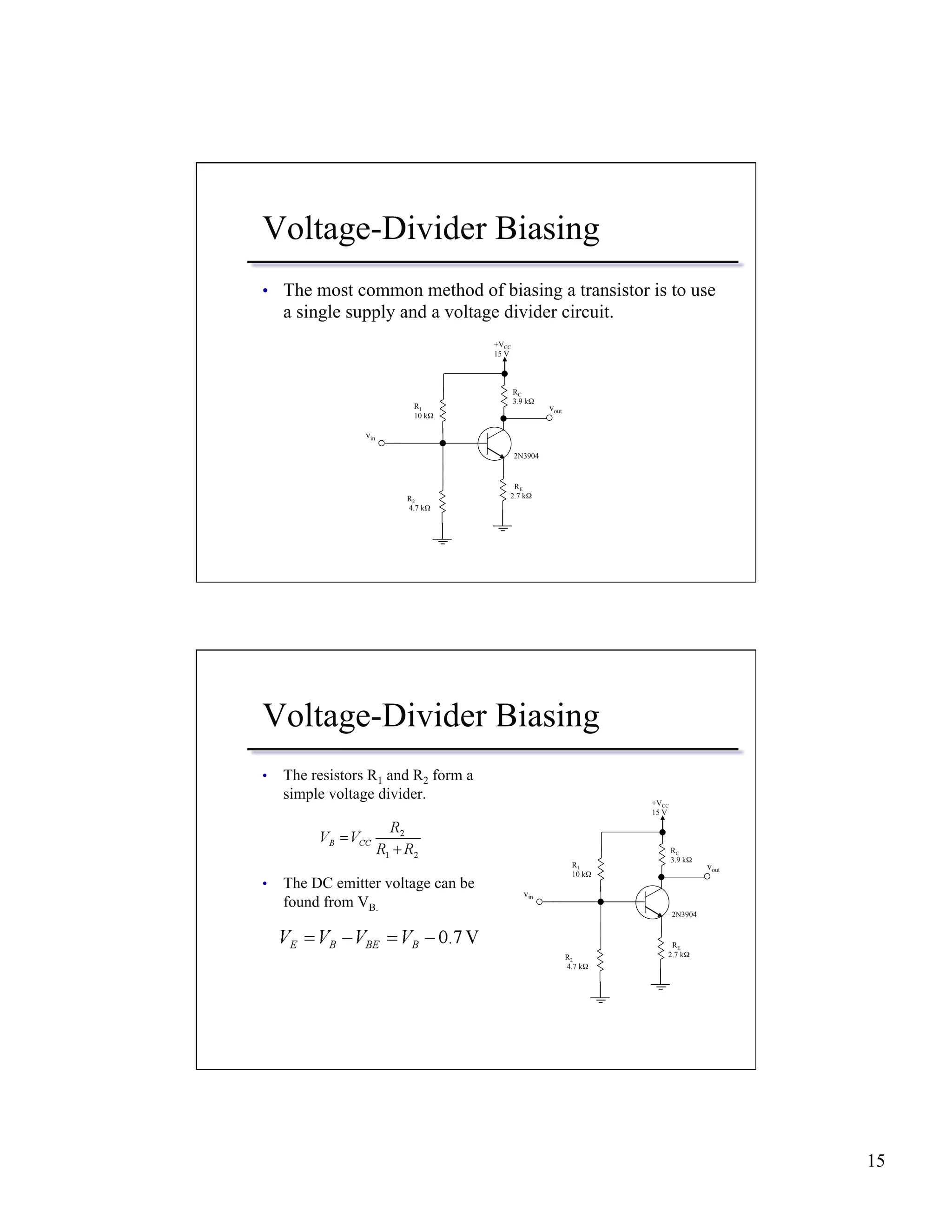
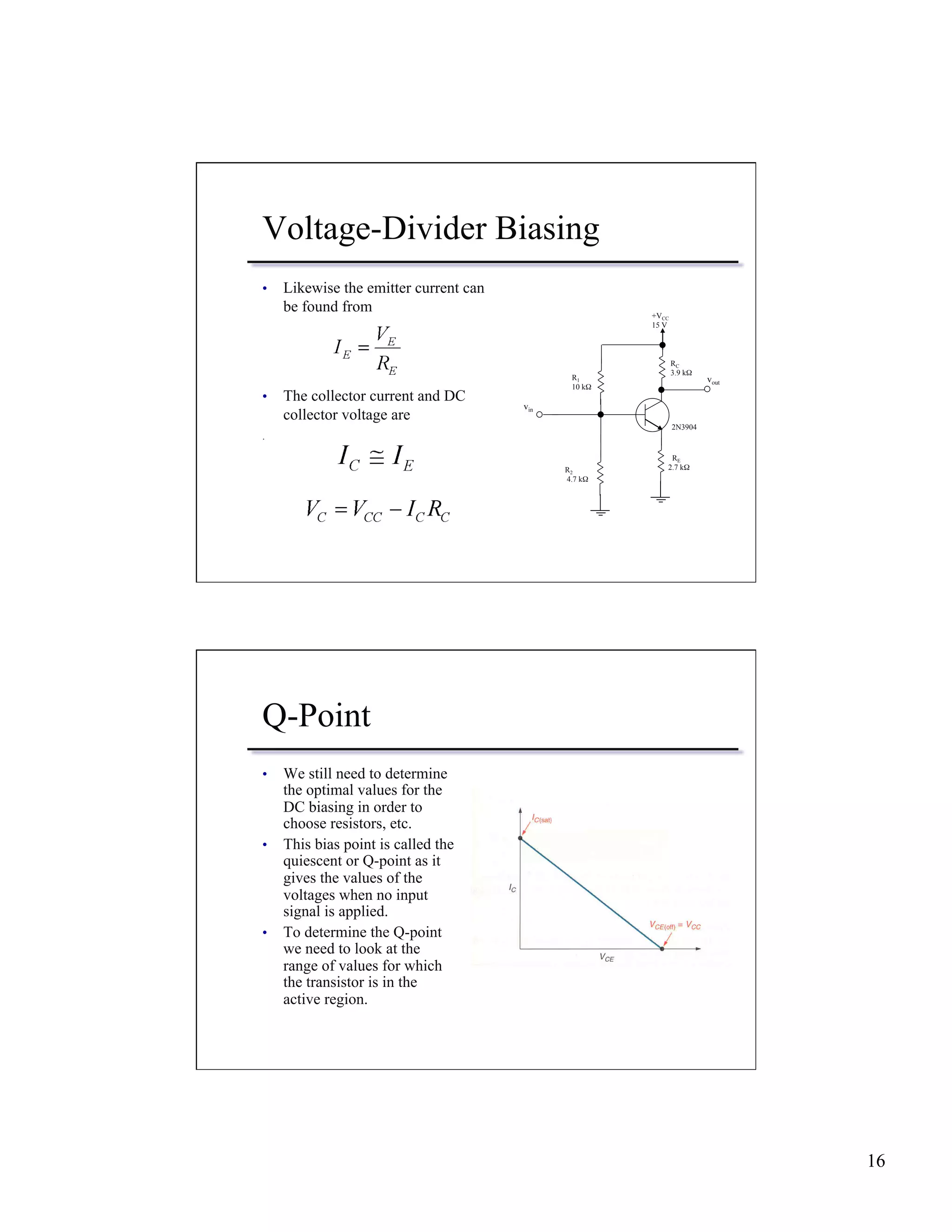
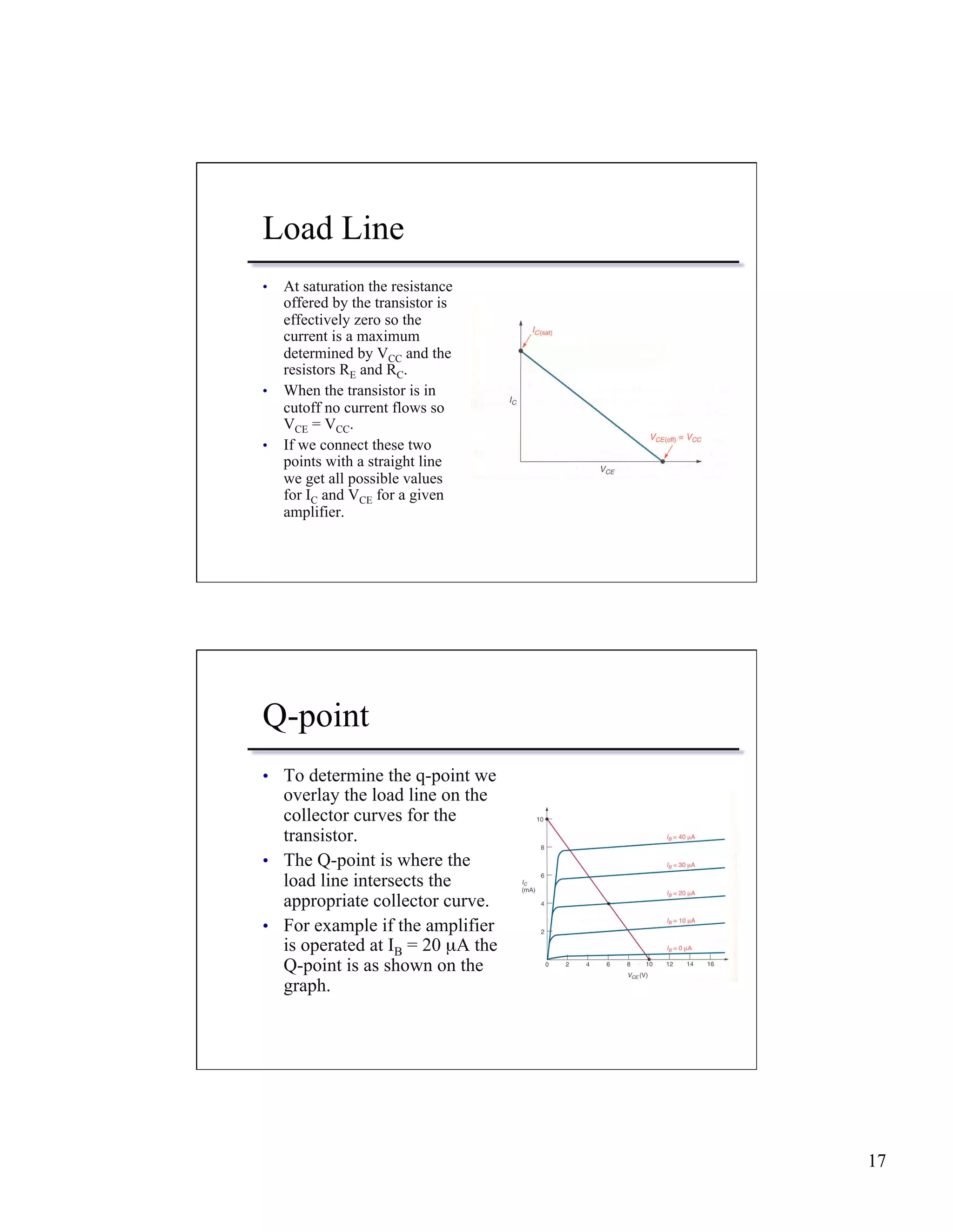

This document provides an overview of bipolar junction transistors (BJT) including: - The basic structure of an NPN or PNP transistor with emitter, base, and collector layers. - How transistors operate in cutoff, saturation, and active modes depending on biasing of the PN junctions. - How a small base current controls a larger collector current in the active region, allowing transistors to function as electronic switches or amplifiers.


