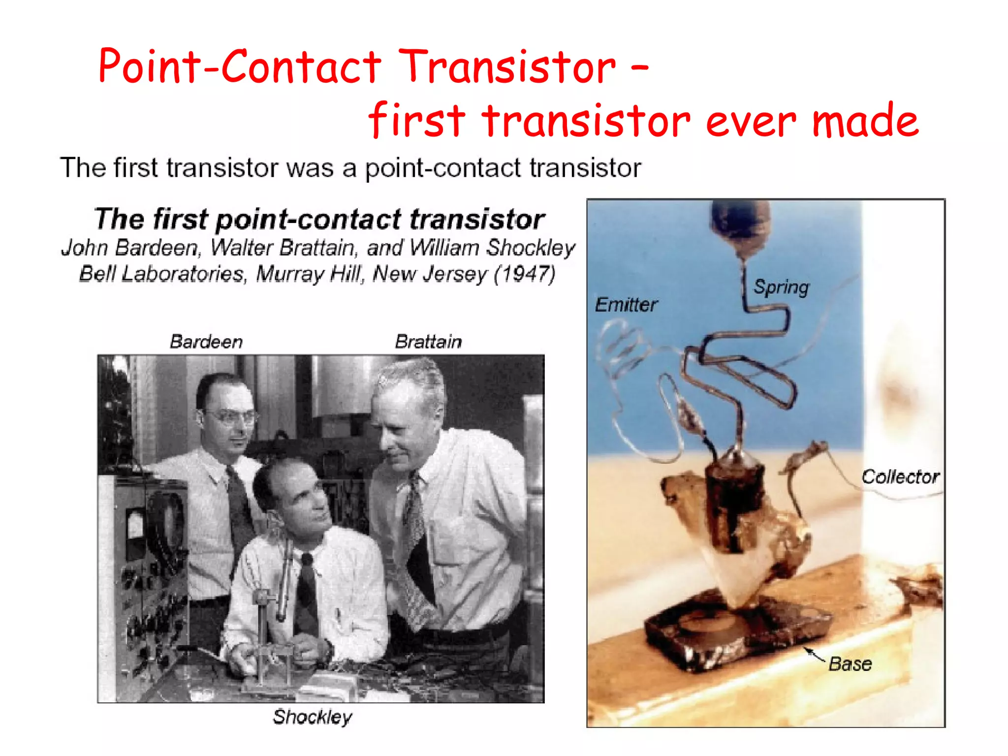
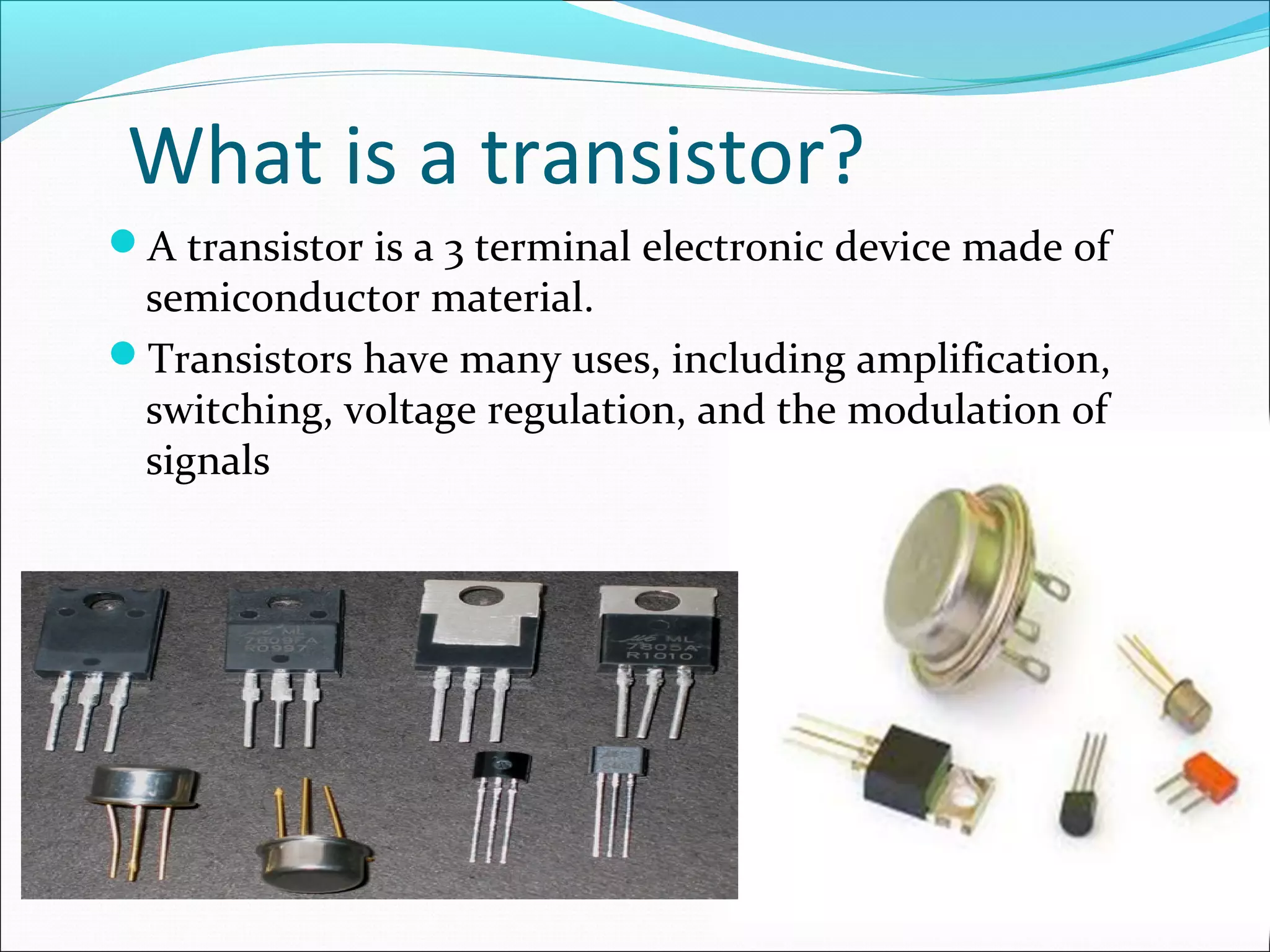
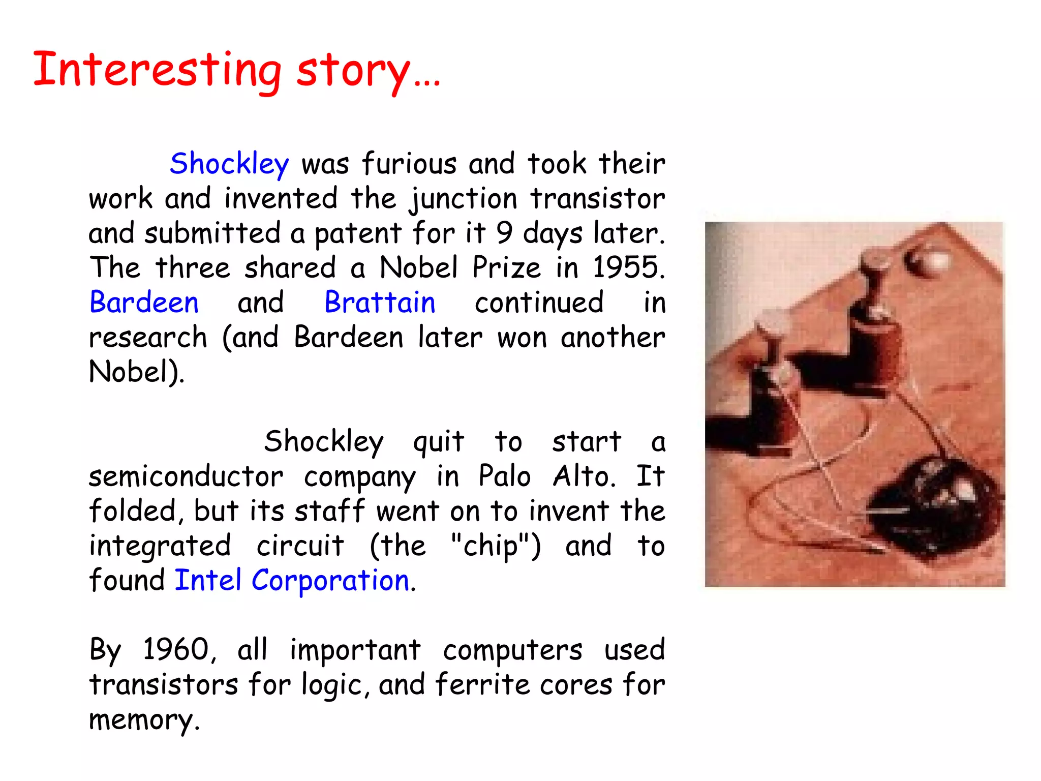
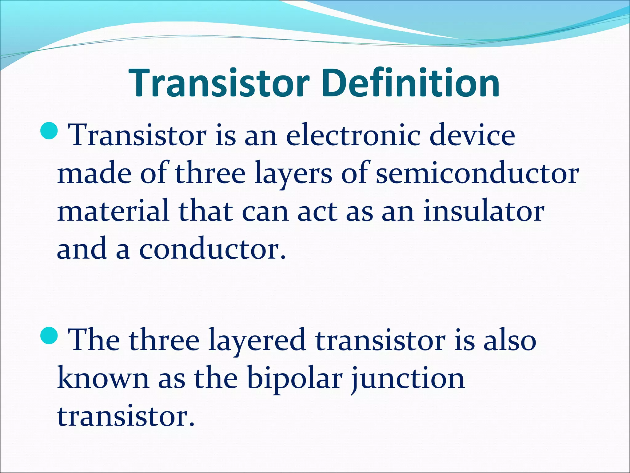
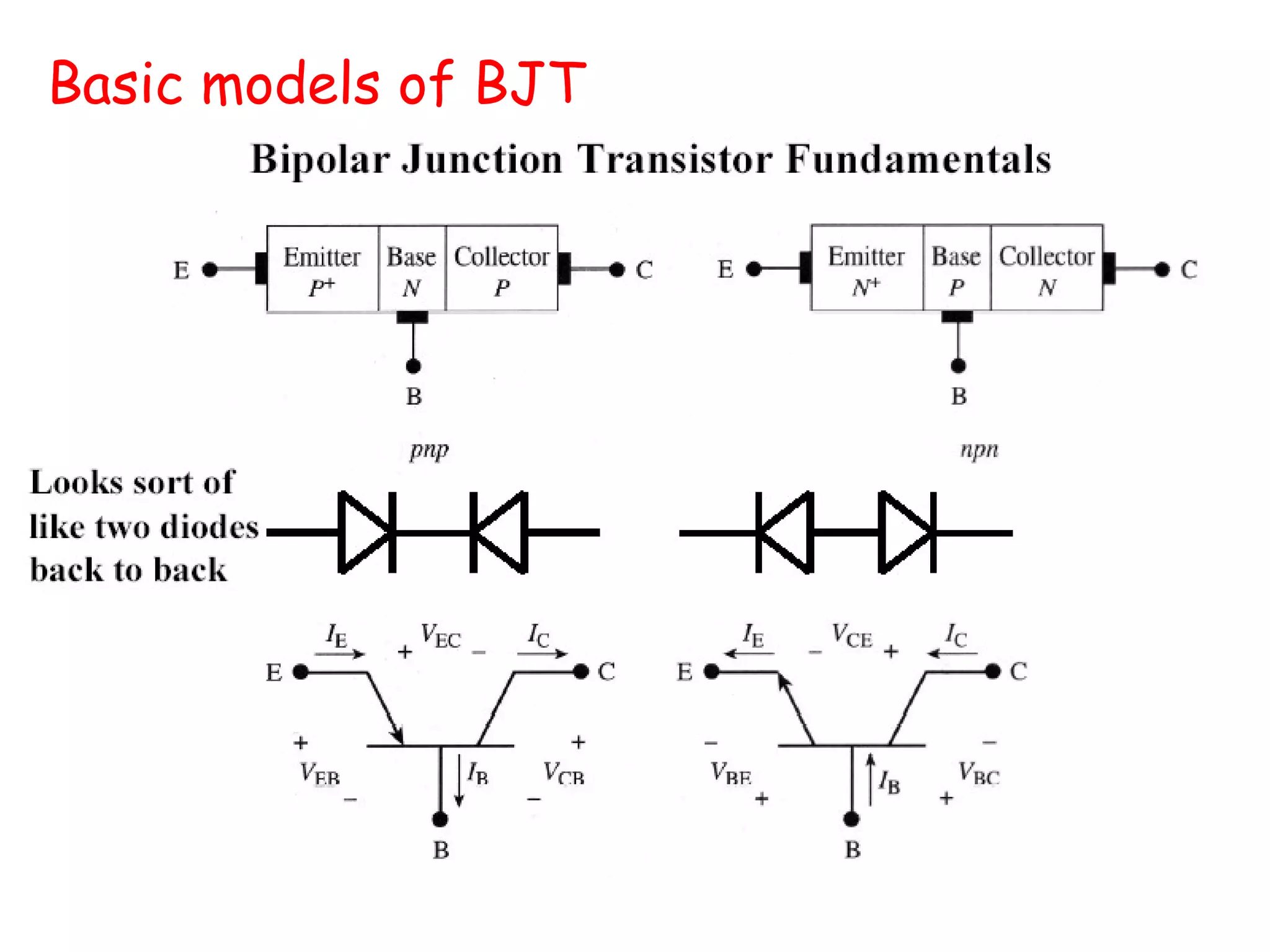
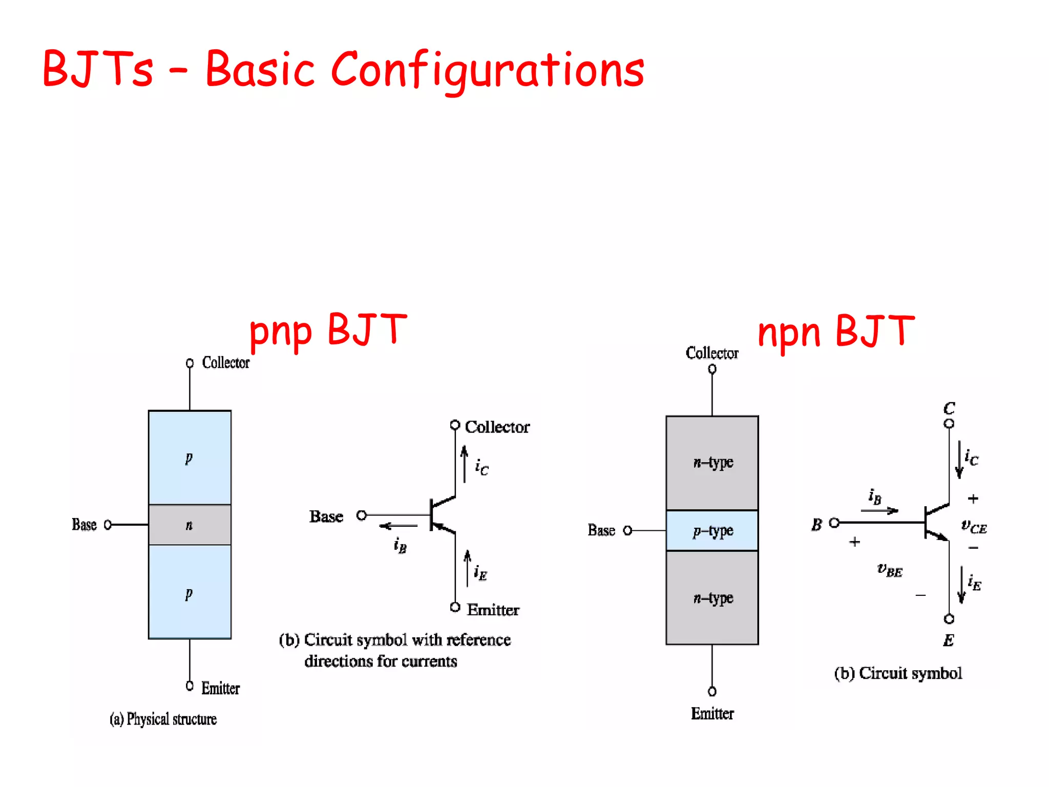
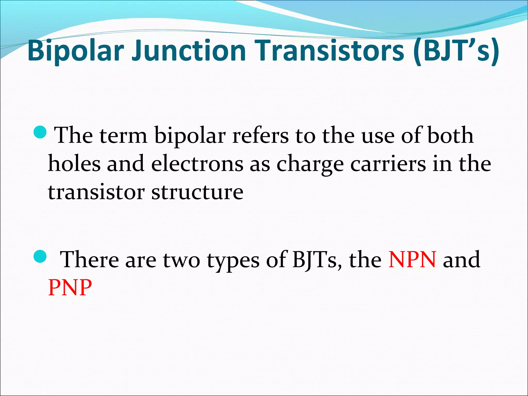
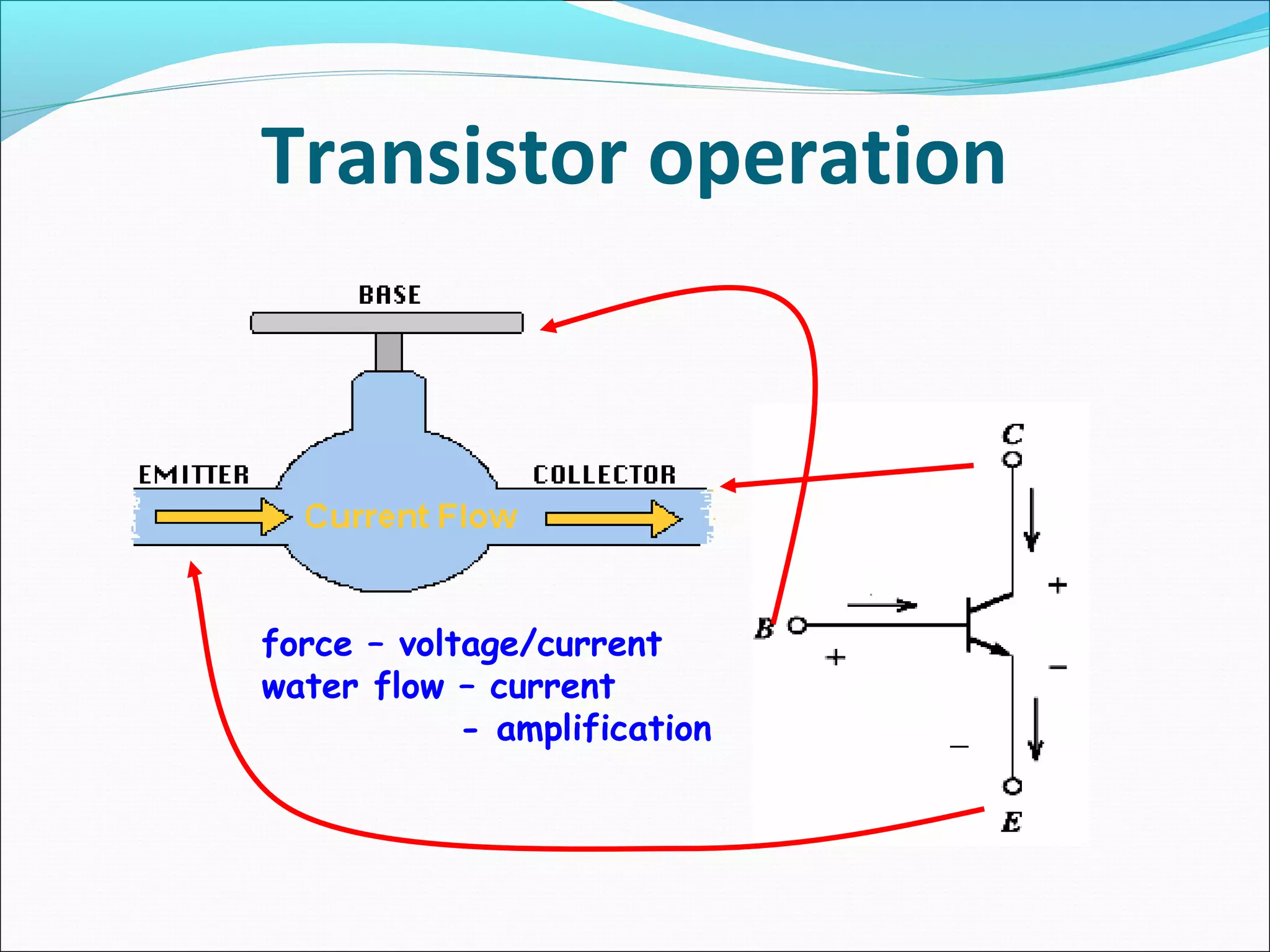
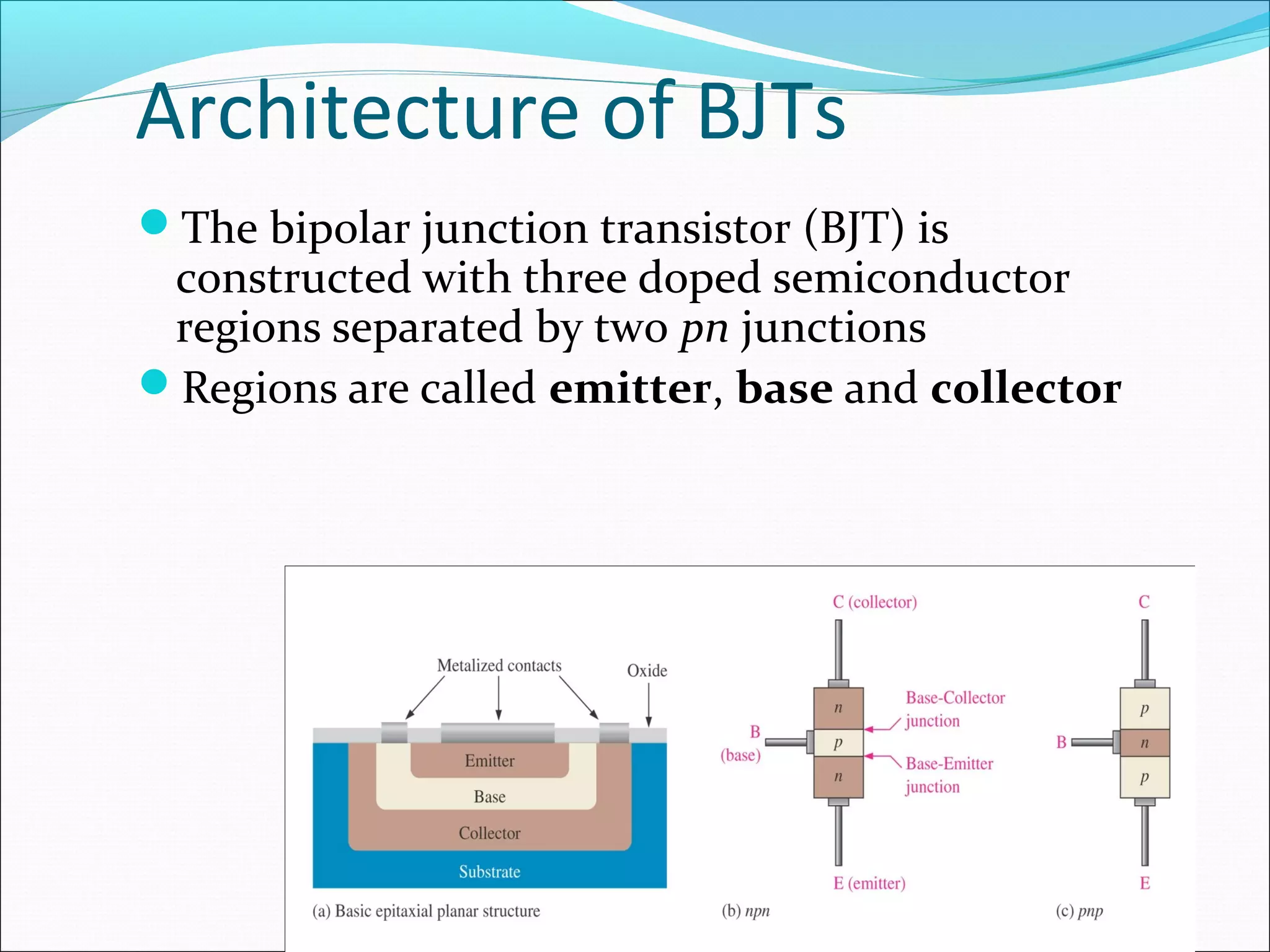
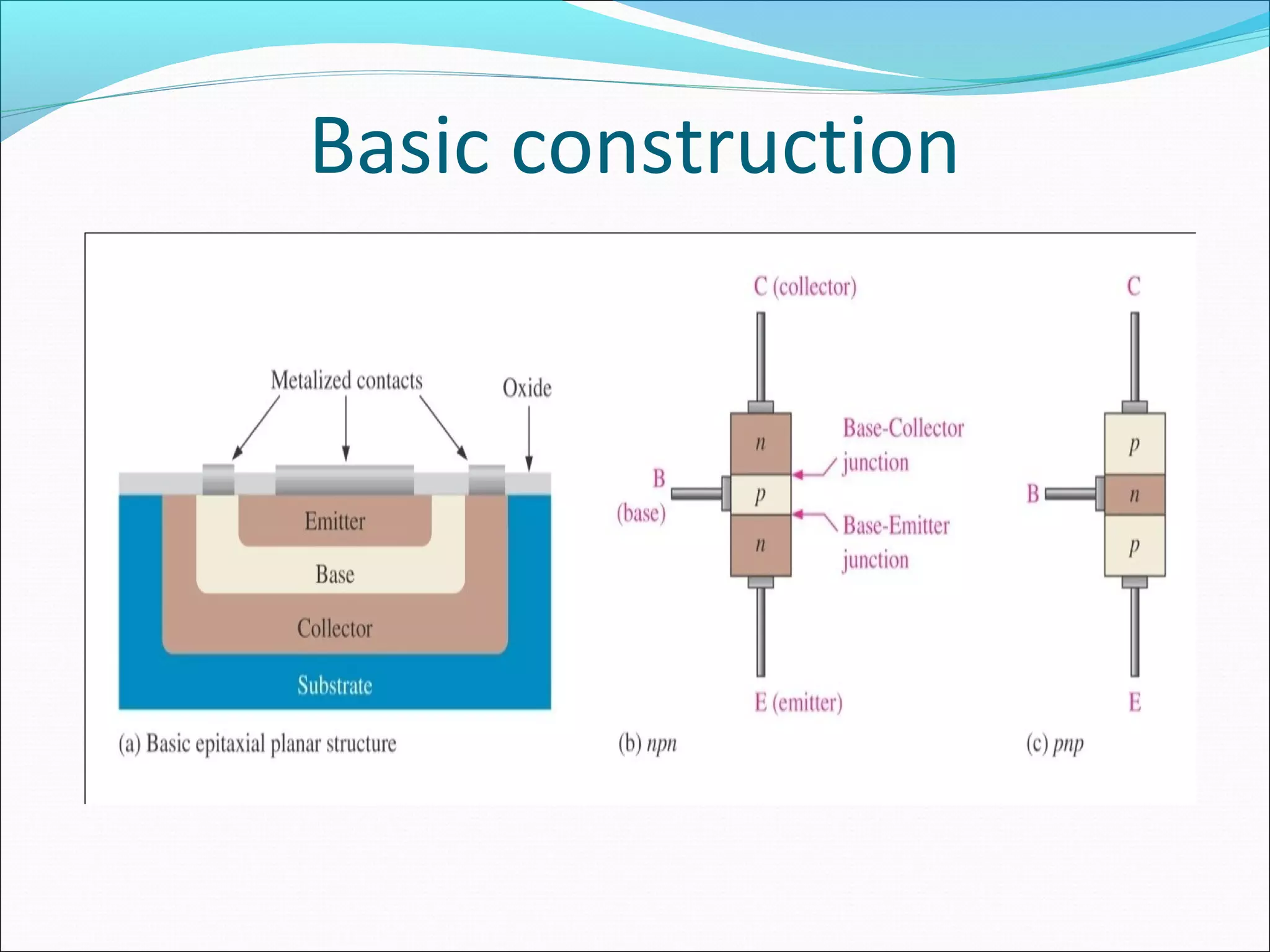
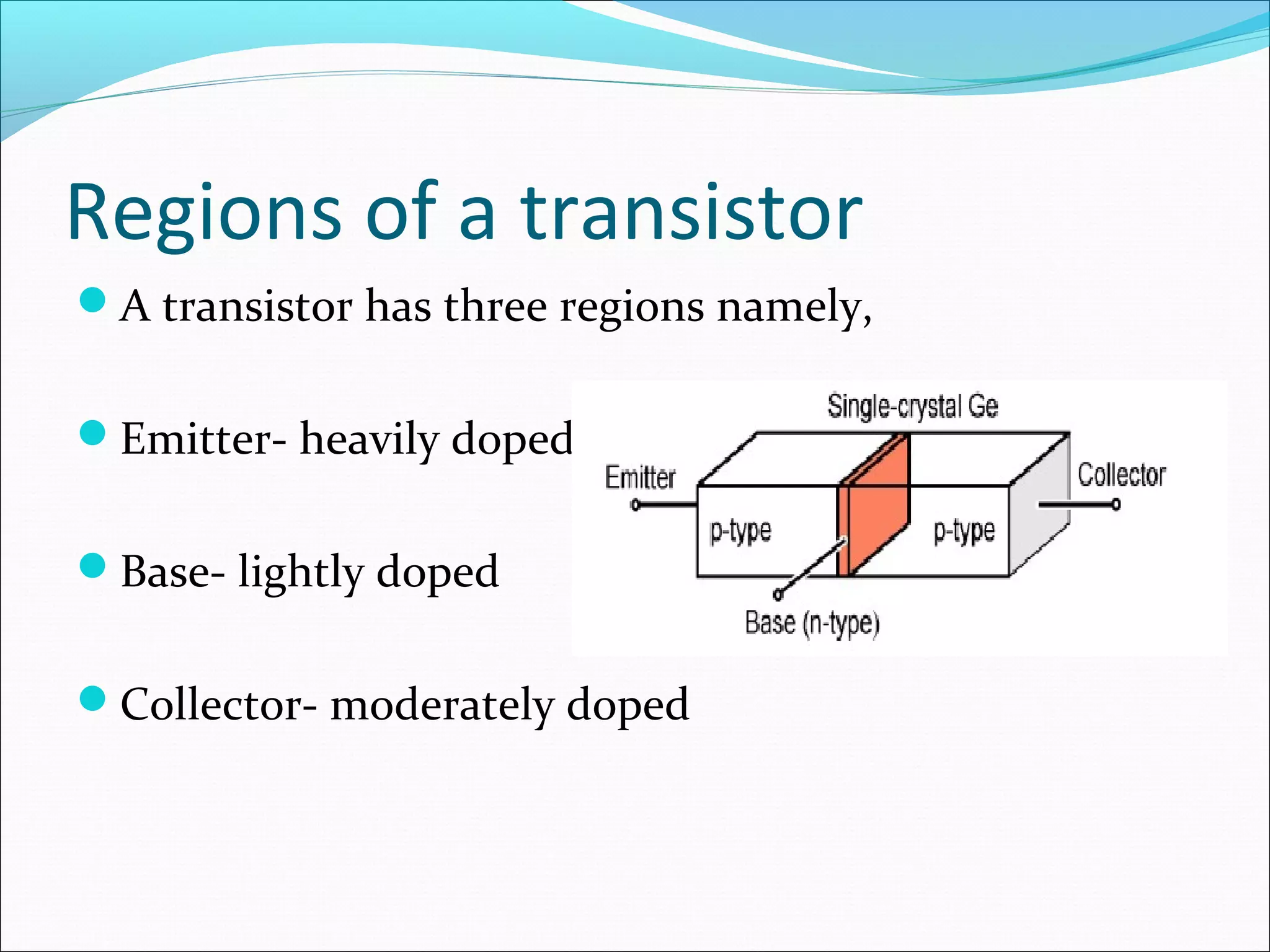
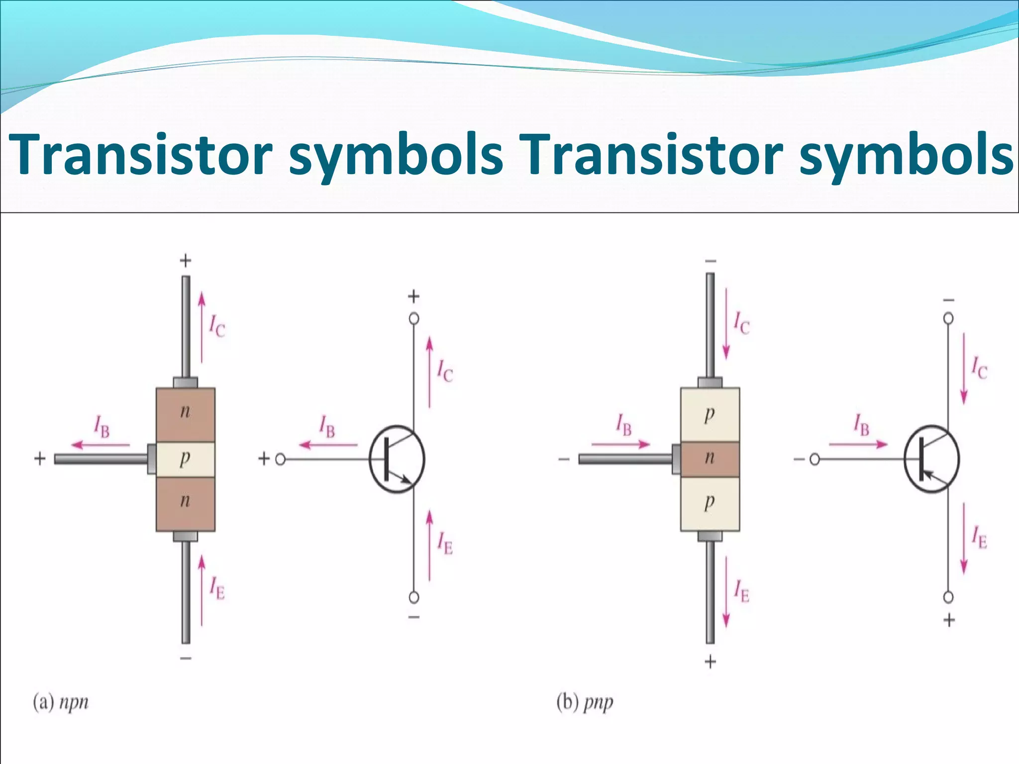
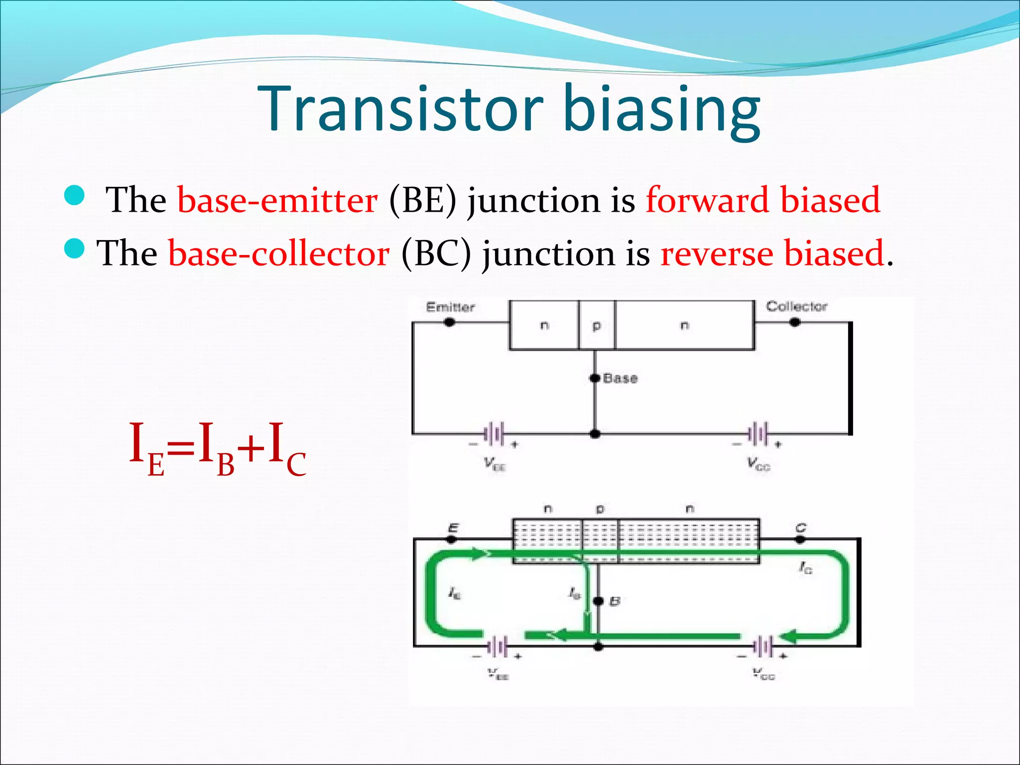
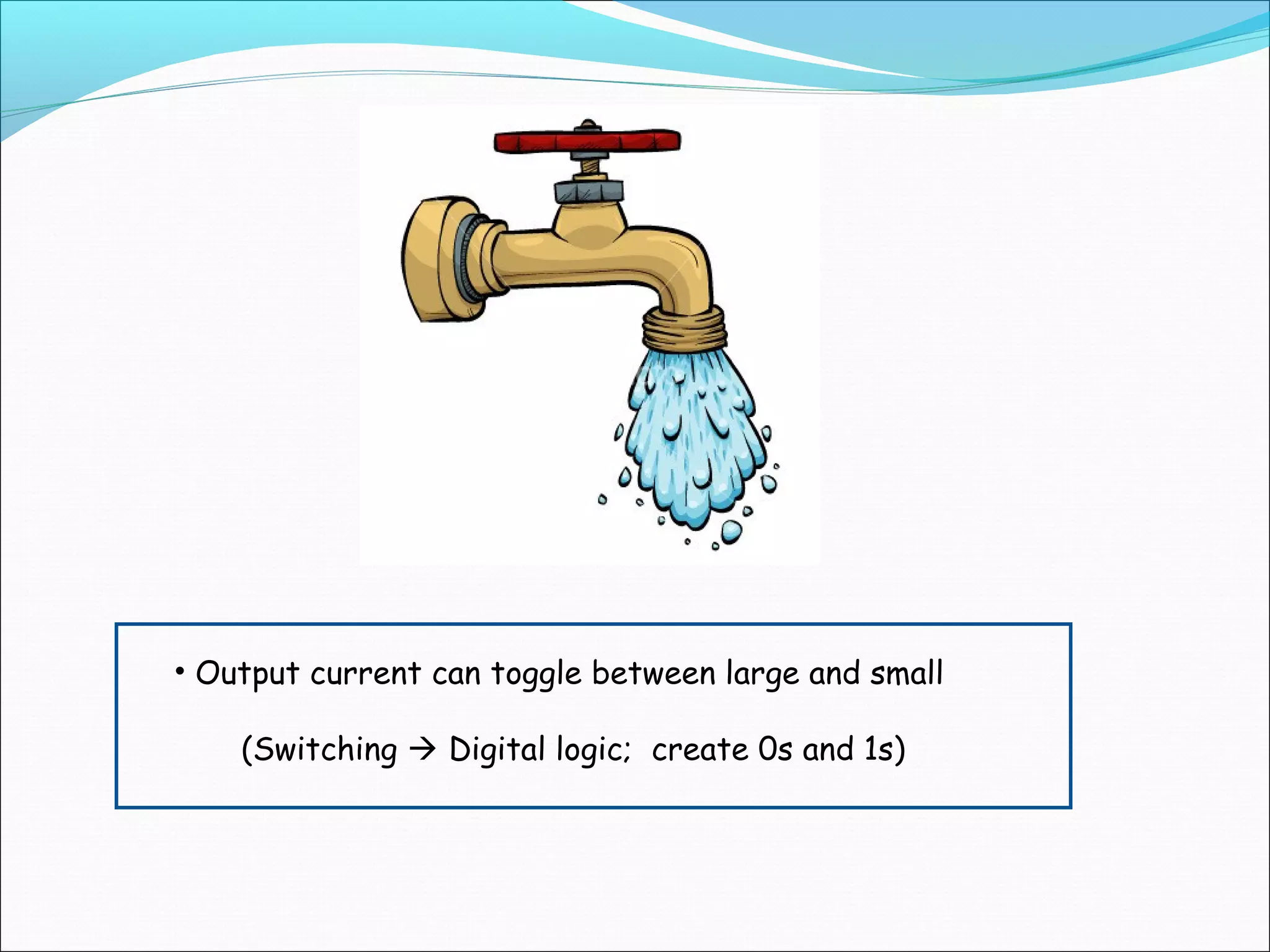
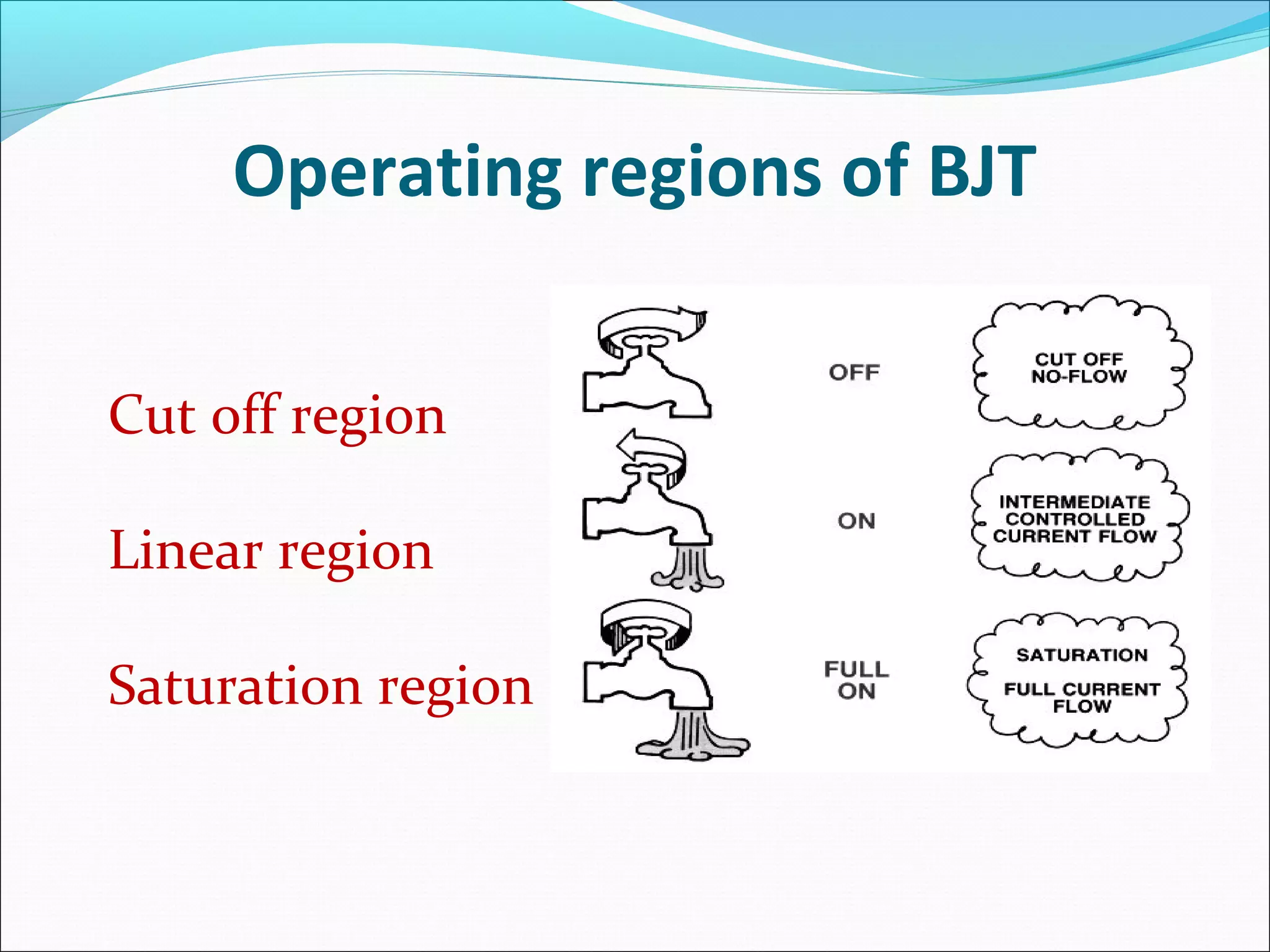
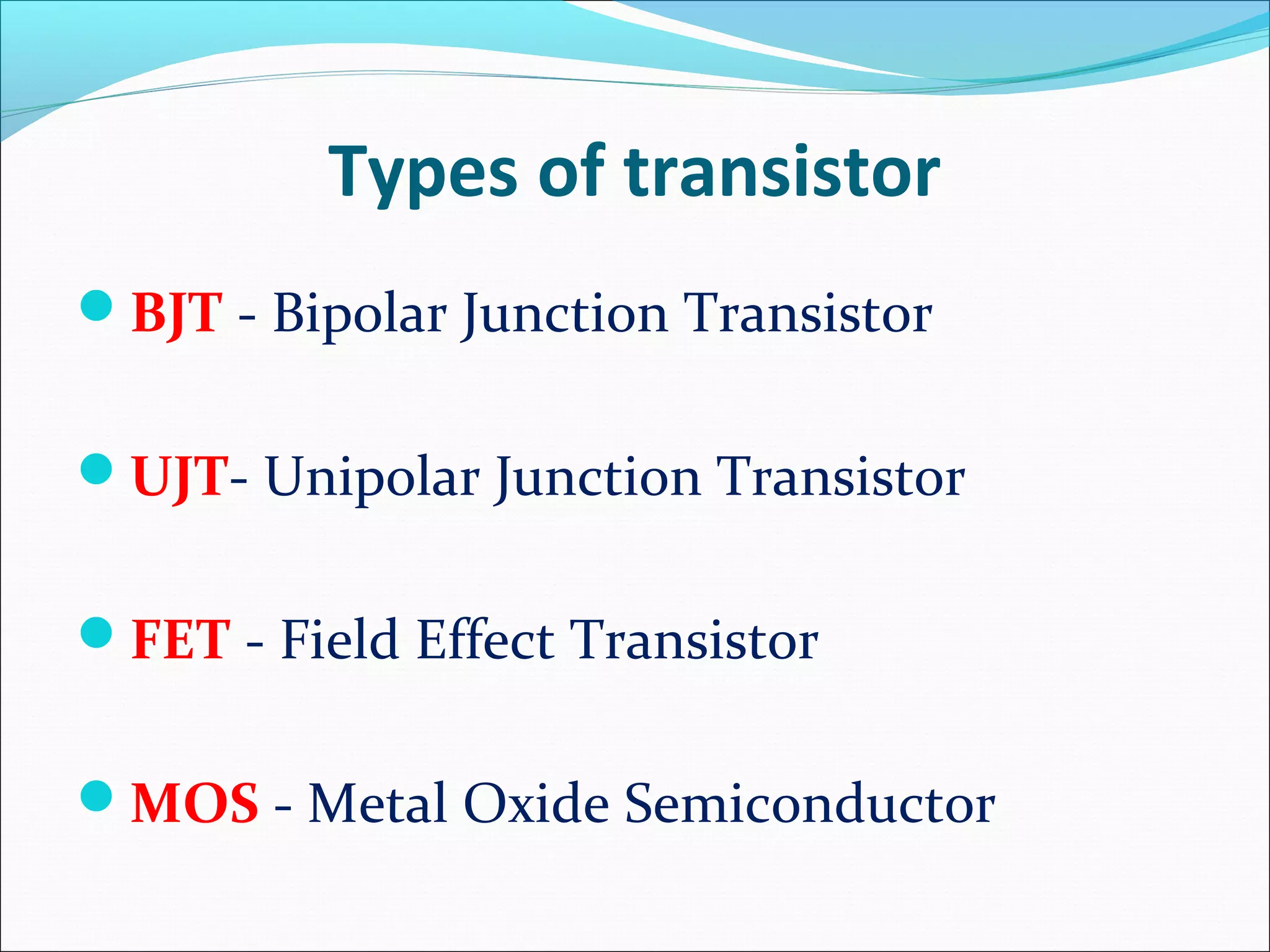
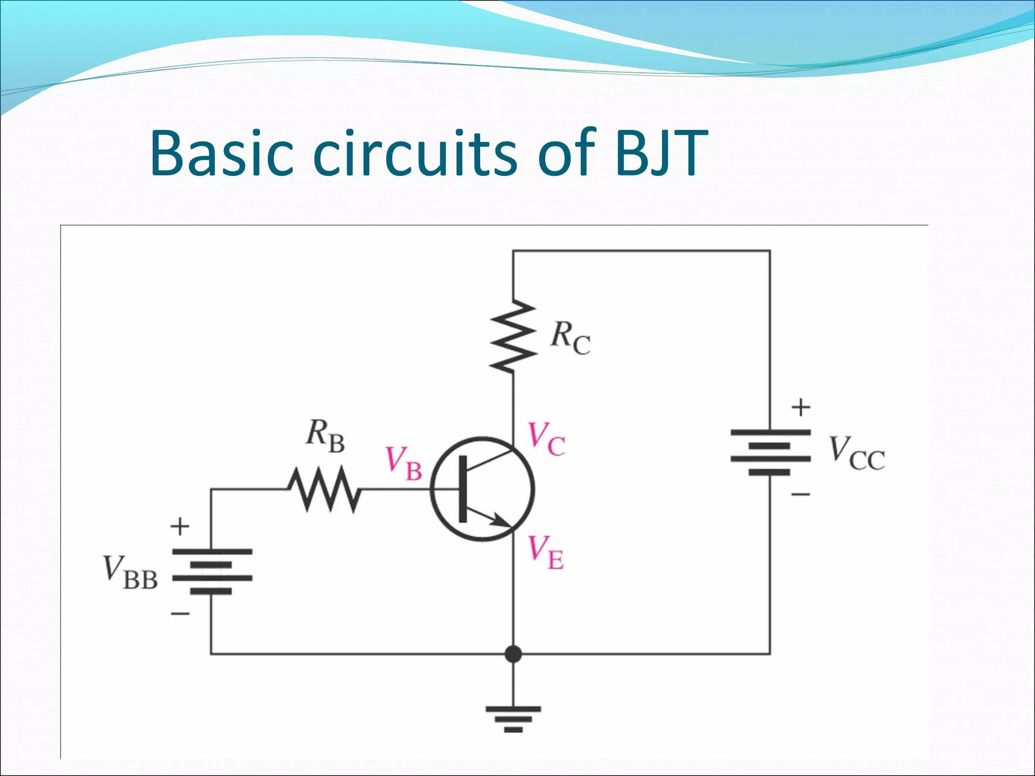
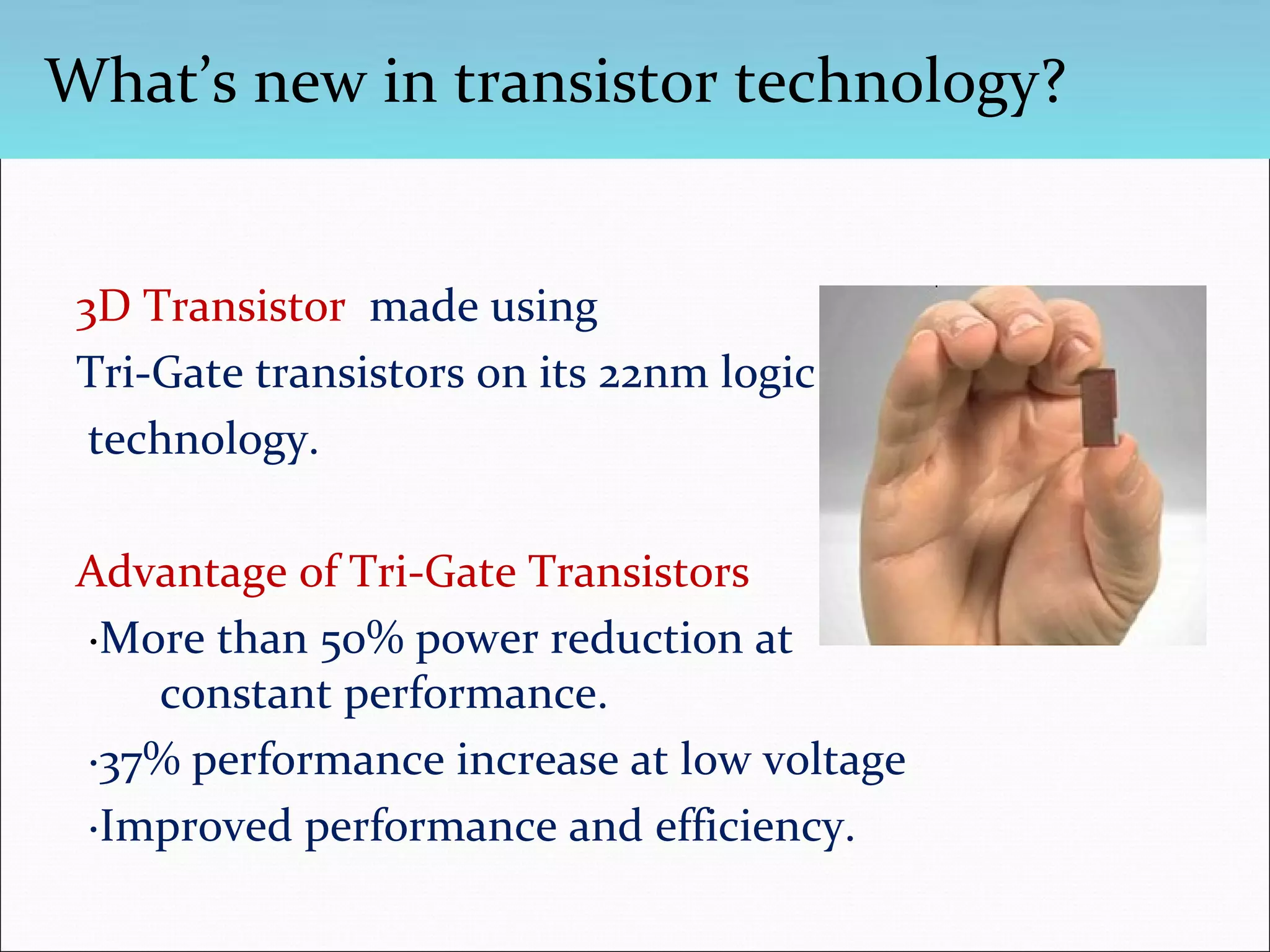
The document discusses the history and operation of transistors, beginning with the point-contact transistor invented in 1947 by Bardeen, Brattain, and Shockley at Bell Labs. It then covers the basic structure and types of bipolar junction transistors, including NPN and PNP, as well as their operating regions and usage as switches and amplifiers. New developments in transistor technology include 3D transistors using tri-gate designs for improved power efficiency and performance.
The study of the basics of electronics can be studied through the link http://bit.ly/2PPv0mv
The transistor is a semiconductor device with three connections, capable of amplification in addition to rectification
Here you find the information about Transistors. And know about
-> Type Of Transistor:
->Region of Transistor:
->P-N Junction Diodes
->Transistor application
->Transistor Connections
Limitation:
->Future of transistor:
The three terminals of the FET are known as Gate, Drain, and Source.
It is a voltage controlled device, where the input voltage controls by the output current.
In FET current used to flow between the drain and the source terminal. And this current can be controlled by applying the voltage between the gate and the source terminal.
So this applied voltage generate the electric field within the device and by controlling these electric field we can control the flow of current through the device.
The MOSFET is an important element in embedded system design which is used to control the loads as per the requirement. The MOSFET is a high voltage controlling device provides some key features for circuit designers in terms of their overall performance.
Introduction to feedback (block diagram and types of feedback) , Analysis at middle, low and high frequency of multi-stage amplifier with RC coupling and direct coupling, cascade amplifiers-Darlington Pair.
Kerala Engineering Architecture Medical is an entrance examination series for admissions to various professional degree courses in the state of Kerala, India. It is conducted by the Office of the Commissioner of Entrance Exams run by the Government of Kerala
Paleontology is the study of the history of life on Earth as based on fossils. Fossils are the remains of plants, animals, fungi, bacteria, and single-celled living things that have been replaced by rock material or impressions of organisms preserved in roc
The ways in which an element—or compound such as water—moves between its various living and nonliving forms and locations in the biosphere is called a biogeochemical cycle. Biogeochemical cycles important to living organisms include the water, carbon, nitrogen, phosphorus, and sulfur cycles.
The AC and DC bridge both are used for measuring the unknown parameter of the circuit. The AC bridge measures the unknown impedance of the circuit. The DC bridge measures the unknown resistance of the circuit.
The Wien bridge is a type of bridge circuit that was developed by Max Wien in 1891. The bridge consists of four resistors and two capacitors. At the time of the Wien bridge's invention, bridge circuits were a common way of measuring component values by comparing them to known values.
For most of us, our name existed even before we did.
In anticipation of our arrival, our parents went through an ultra stressful process of narrowing down dozens of potential names until they chose the perfect one.
Luckily they did, because whatever your name is, it has followed you throughout your entire life; and in some cases, people may have heard of your name before they’ve ever met you.
When it comes to how to name an app, it’s of similar importance as naming a child. The name of your app will follow your brand forever, and in many cases, potential users will hear the name before they ever actually use your app.
flora and fauna of himachal pradesh and keralaAJAL A J
flora and fauna of himachal pradesh and kerala
A green pearl in the Himalayan crown, Himachal Pradesh is blessed with a rich flora and fauna that graces the land with grandeur and majesty. Other animals that can be sighted in the wild include the ibex, wild yak, ghoral deer, musk deer, Himalayan black bear, brown bear, leopards and the Himalayan Thar. Also kerala is gods on country
Bachelor of Science in Cardio-vascular technology is an undergraduate course in cardiology. These technologists assist the physicians in the diagnosis and the treatment of cardiac (heart) and peripheral vascular conditions (blood vessels). The cardiovascular technologists are also responsible for preparing the patients for open-heart surgeries and pacemaker implantation surgeries. The technologists also monitor the patient’s cardiac parameters while they undergo the surgery. B. Sc. in Cardiovascular technology is a three years’ full-time undergraduate course and is an interesting and important course in medicine.
`Remove Unprofitable Products and Services. The products or services with the highest gross profit margin are the most important to your business. ...
Find New Customers. New customers can help grow your business. ...
Increase your Conversion Rate. ...
Review Current Pricing Structure. ...
Reduce your inventory. ...
Reduce your overheads.
Polycystic ovary syndrome (PCOS) is a hormonal disorder common among women of reproductive age. Women with PCOS may have infrequent or prolonged menstrual periods or excess male hormone (androgen) levels. The ovaries may develop numerous small collections of fluid (follicles) and fail to regularly release eggs
Are you an NRI and aiming to come back to India to pursue graduation from the top-tier colleges of India?
Then, you’re halfway there. Being an NRI, your top preference would be IITs and NITs of India. If that's the case, you must know the fee structure of both the IITs, NITs (under DASA scheme), Centrally Funded Institutions and State-Level Govt. Engineering Colleges.
Note: According to the latest update from DASA, from session 2021-22 onwards, JEE Rank is made mandatory for NRI/PIO/OCI Students to be eligible for DASA & CIWG Schemes. Hence, 2020-21 will be the last year when SAT 2 scores will be considered for DASA/CIWG Scheme.
Subjects to study if you want to work for a charityAJAL A J
The charity sector can be competitive and experience, volunteer or otherwise, can count for a lot. But there are ways to make that third sector CV stand out from the competition. Why not take some courses? A course can be a great way to make your application shine and an opportunity to learn new skills and ideas.
Joint Entrance Examination - Main or commonly known as JEE Main is a national level entrance exam conducted by the NTA to offer admission to BE/BTech, BPlan and BArch courses at the IIITs (Indian Institute of Information Technology), NITs (National Institute of Technology) and other Centrally Funded Technical Institutions (CFTIs) across the country.
Hybrid optimization of pumped hydro system and solar- Engr. Abdul-Azeez.pdffxintegritypublishin
Advancements in technology unveil a myriad of electrical and electronic breakthroughs geared towards efficiently harnessing limited resources to meet human energy demands. The optimization of hybrid solar PV panels and pumped hydro energy supply systems plays a pivotal role in utilizing natural resources effectively. This initiative not only benefits humanity but also fosters environmental sustainability. The study investigated the design optimization of these hybrid systems, focusing on understanding solar radiation patterns, identifying geographical influences on solar radiation, formulating a mathematical model for system optimization, and determining the optimal configuration of PV panels and pumped hydro storage. Through a comparative analysis approach and eight weeks of data collection, the study addressed key research questions related to solar radiation patterns and optimal system design. The findings highlighted regions with heightened solar radiation levels, showcasing substantial potential for power generation and emphasizing the system's efficiency. Optimizing system design significantly boosted power generation, promoted renewable energy utilization, and enhanced energy storage capacity. The study underscored the benefits of optimizing hybrid solar PV panels and pumped hydro energy supply systems for sustainable energy usage. Optimizing the design of solar PV panels and pumped hydro energy supply systems as examined across diverse climatic conditions in a developing country, not only enhances power generation but also improves the integration of renewable energy sources and boosts energy storage capacities, particularly beneficial for less economically prosperous regions. Additionally, the study provides valuable insights for advancing energy research in economically viable areas. Recommendations included conducting site-specific assessments, utilizing advanced modeling tools, implementing regular maintenance protocols, and enhancing communication among system components.
Student information management system project report ii.pdfKamal Acharya
Our project explains about the student management. This project mainly explains the various actions related to student details. This project shows some ease in adding, editing and deleting the student details. It also provides a less time consuming process for viewing, adding, editing and deleting the marks of the students.
Industrial Training at Shahjalal Fertilizer Company Limited (SFCL)MdTanvirMahtab2
This presentation is about the working procedure of Shahjalal Fertilizer Company Limited (SFCL). A Govt. owned Company of Bangladesh Chemical Industries Corporation under Ministry of Industries.
Immunizing Image Classifiers Against Localized Adversary Attacksgerogepatton
This paper addresses the vulnerability of deep learning models, particularly convolutional neural networks
(CNN)s, to adversarial attacks and presents a proactive training technique designed to counter them. We
introduce a novel volumization algorithm, which transforms 2D images into 3D volumetric representations.
When combined with 3D convolution and deep curriculum learning optimization (CLO), itsignificantly improves
the immunity of models against localized universal attacks by up to 40%. We evaluate our proposed approach
using contemporary CNN architectures and the modified Canadian Institute for Advanced Research (CIFAR-10
and CIFAR-100) and ImageNet Large Scale Visual Recognition Challenge (ILSVRC12) datasets, showcasing
accuracy improvements over previous techniques. The results indicate that the combination of the volumetric
input and curriculum learning holds significant promise for mitigating adversarial attacks without necessitating
adversary training.
Sachpazis:Terzaghi Bearing Capacity Estimation in simple terms with Calculati...Dr.Costas Sachpazis
Terzaghi's soil bearing capacity theory, developed by Karl Terzaghi, is a fundamental principle in geotechnical engineering used to determine the bearing capacity of shallow foundations. This theory provides a method to calculate the ultimate bearing capacity of soil, which is the maximum load per unit area that the soil can support without undergoing shear failure. The Calculation HTML Code included.
2. The Wonder child of electronics By
AJAL.A.J ( ASSISTANT PROFESSOR)
ECE DEPARTMENT
MAIL: ec2reach@gmail.com
MOB: 8907305642
3. What is a transistor?
A transistor is a 3 terminal electronic device made of
semiconductor material.
Transistors have many uses, including amplification,
switching, voltage regulation, and the modulation of
signals
4. This session will help you to
understand the,
1.Evolution of transistor
2.Importance of transistor
3.Definition & transistor types
4.Transistor symbol & operation
5.Advantages of transistor
6.Latest in transistor technology
5. History of transistors
In 1906, an American inventor and physicist,
Lee De Forest, made the vacuum tube
triode or audion as he called it.
Used in radios
Used in early computers
6. Interesting story…
Picture shows the workbench of John
Bardeen (Stocker Professor at OU) and
Walter Brattain at Bell Laboratories. They
were supposed to be doing fundamental
research about crystal surfaces.
The experimental results hadn't been
very good, though, and there's a rumor that
their boss, William Shockley, came near to
canceling the project. But in 1947, working
alone, they switched to using tremendously
pure materials.
It dawned on them that they could
build the circuit in the picture. It was a
working amplifier! John and Walter
submitted a patent for the first working point
contact transistor.
7. Interesting story…
Shockley was furious and took their
work and invented the junction transistor
and submitted a patent for it 9 days later.
The three shared a Nobel Prize in 1955.
Bardeen and Brattain continued in
research (and Bardeen later won another
Nobel).
Shockley quit to start a
semiconductor company in Palo Alto. It
folded, but its staff went on to invent the
integrated circuit (the "chip") and to
found Intel Corporation.
By 1960, all important computers used
transistors for logic, and ferrite cores for
memory.
10. First Bipolar Junction Transistors
W. Shockley invented the p-n junction transistor
The physically relevant region is moved to the bulk of the material
11. Moore’s Law
It’s an observation made by Gordon E. Moore, in
which he predicted that the number of transistors,
inside an Integrated Circuit, could
be doubled every 24 months.
At the density that also
minimized the cost of a transistor.
12. Transistor Definition
Transistor is an electronic device
made of three layers of semiconductor
material that can act as an insulator
and a conductor.
The three layered transistor is also
known as the bipolar junction
transistor.
15. Bipolar Junction Transistors (BJT’s)
The term bipolar refers to the use of both
holes and electrons as charge carriers in the
transistor structure
There are two types of BJTs, the NPN and
PNP
16. Origin of the names
the Emitter 'emits' the electrons which pass through
the device
the Collector 'collects' them again once they've
passed through the Base
...and the Base?...
18. Architecture of BJTs
The bipolar junction transistor (BJT) is
constructed with three doped semiconductor
regions separated by two pn junctions
Regions are called emitter, base and collector
20. Architecture of BJTs
There are two types of BJTs, the npn and pnp
The two junctions are termed the base-emitter junction
and the base-collector junction
The term bipolar refers to the use of both holes and
electrons as charge carriers in the transistor structure
In order for the transistor to operate properly, the two
junctions must have the correct dc bias voltages
the base-emitter (BE) junction is forward
biased(>=0.7V for Si, >=0.3V for Ge)
the base-collector (BC) junction is reverse biased
21. Regions of a transistor
A transistor has three regions namely,
Emitter- heavily doped
Base- lightly doped
Collector- moderately doped
31. Operation of BJTs
BJT will operates in one of following four region
Cutoff region (for digital circuit)
Saturation region (for digital circuit)
Linear (active) region (to be an amplifier)
Breakdown region (always be a disaster)
32.
33. DC Analysis of BJTs
Transistor Currents: IE = IC + IB
alpha (aDC) IC = aDCIE
beta (bDC) IC = bDCIB
bDC typically has a value between 20 and 200
34. DC Analysis of BJTs
DC voltages for the biased
transistor:
Collector voltage
VC = VCC - ICRC
Base voltage
VB = VE + VBE
for silicon transistors, VBE = 0.7 V
for germanium transistors, VBE = 0.3 V
35. Q-point
The base current, IB, is established by the base
bias
The point at which the base current curve
intersects the dc load line is the quiescent or Q-point
for the circuit
37. DC Analysis of BJTs
The voltage divider
biasing is widely used
Input resistance is:
RIN @ bDCRE
The base voltage is
approximately:
VB @ VCCR2/(R1+R2)
38. BJT as an amplifier
Class A Amplifiers
Class B Amplifiers
40. BJT Class A Amplifiers
In a class A amplifier, the transistor conducts for the
full cycle of the input signal (360°)
used in low-power applications
The transistor is operated in the active region,
between saturation and cutoff
saturation is when both junctions are forward biased
the transistor is in cutoff when IB = 0
The load line is drawn on the collector curves between
saturation and cutoff
42. BJT Class A Amplifiers
Three biasing mode for class A amplifiers
common-emitter (CE) amplifier
common-collector (CC) amplifier
common-base (CB) amplifier
43. BJT Class A Amplifiers
A common-emitter (CE) amplifier
capacitors are used for coupling ac without disturbing dc
levels
44. BJT Class A Amplifiers
A common-collector (CC) amplifier
voltage gain is approximately 1, but current gain is
greater than 1
45. BJT Class A Amplifiers
BJT Class A Amplifiers
The third configuration is the common-base (CB)
the base is the grounded (common) terminal
the input signal is applied to the emitter
output signal is taken off the collector
output is in-phase with the input
voltage gain is greater than 1
current gain is always less than 1
47. BJT Class B Amplifiers
When an amplifier is biased such that it operates in the
linear region for 180° of the input cycle and is in cutoff for
180°, it is a class B amplifier
A class B amplifier is more efficient than a class A
In order to get a linear reproduction of the input
waveform, the class B amplifier is configured in a push-pull
arrangement
The transistors in a class B amplifier must be biased
above cutoff to eliminate crossover distortion
48.
49. The BJT as a Switch
When used as an electronic switch, a transistor
normally is operated alternately in cutoff and
saturation
A transistor is in cutoff when the base-emitter junction
is not forward-biased. VCE is approximately equal to VCC
When the base-emitter junction is forward-biased and
there is enough base current to produce a maximum
collector current, the transistor is saturated
52. Transistor applications
Transistor as a switch
When used as an electronic switch, the transistor is
normally operated alternately in cut-off and
saturation regions.
53. Transistor as amplifier
Due to the small changes in
base current the collector
current will mimic the input
with greater amplitude
54. Future of Transistors
Molecular electronics
Carbon nanotube transistors
Nano inspiration wire transistors
Quantum computing
CMOS devices will add functionality to CMOS non-volatile
memory, opto-electronics, sensing….
CMOS technology will address new markets
macroelectronics, bio-medical devices, …
Biology may provide for new technologies bottom-up
assembly, human intelligence
55. What’s new in transistor technology?
3D Transistor made using
Tri-Gate transistors on its 22nm logic
technology.
Advantage of Tri-Gate Transistors
·More than 50% power reduction at
constant performance.
·37% performance increase at low voltage
·Improved performance and efficiency.