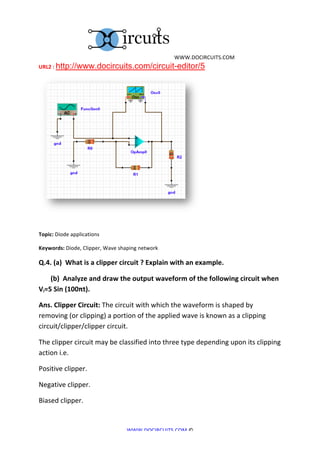
Downloaded 175 times
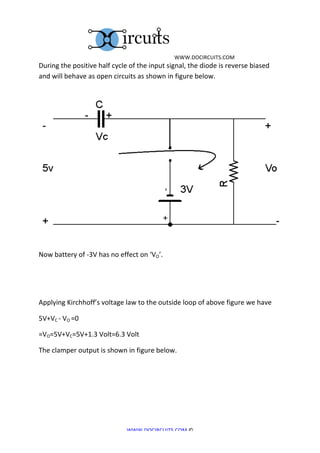
![WWW.DOCIRCUITS.COM
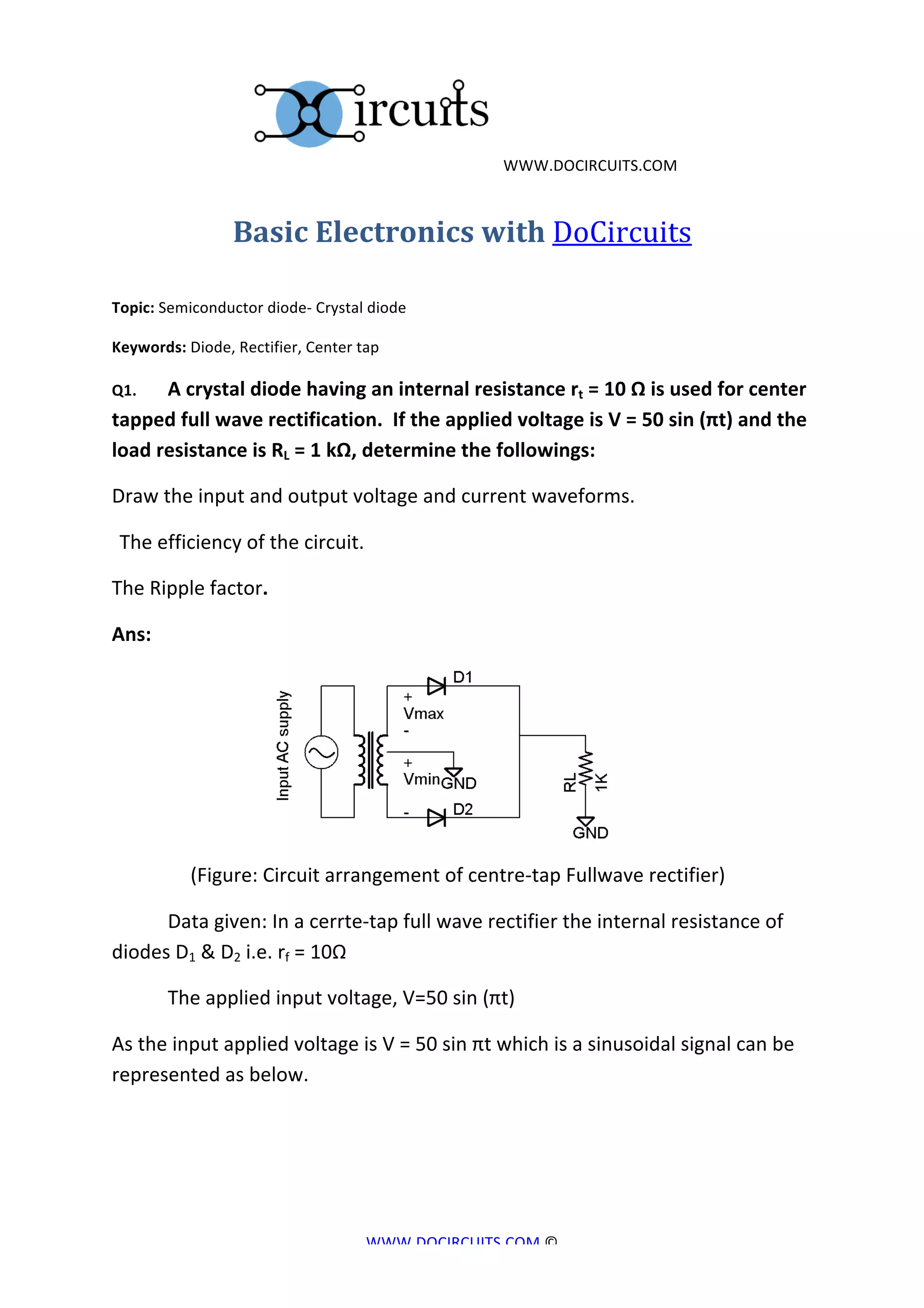
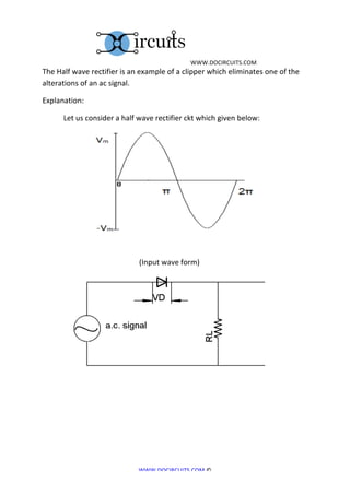
(Output
wave
form)
(Figure
–
b)
Consider
diode
is
an
ideal
diode
[i.e
it
becomes
short
circuit
when
it
will
forward
bias
i.e
VD
>
0
volt
and
open
circuit
when
it
will
reverse
bias
VD<0V,
where
VD
is
the
voltage
across
diode]
So
during
the
+Ve
half
cycle
of
an
i/p
ac
signal
(ie
from
0
to
π)
the
diode
will
be
forward
bias
&
make
it
short
circuited.
So
that
there
will
be
a
current
which
flow
through
‘RL’
So
that
we
can
obtain
an
output
voltage
which
shown
in
figure
(b).
But
during
negative
half
cycle
of
an
signal
(ie
from
‘π’
to
2π)
the
diode
becomes
reverse
bias
so
it
makes
an
open
circuited.
As
a
result
the
current
flow
through
diode
is
zero.
Hence
the
output
voltage
is
zero
during
this
period.
N.B.:
From
the
input
&
Output
waveform
it
is
clear
that
by
help
of
the
above
circuit
we
can
obtain
the
output
during
+ve
cycle
only
not
in
negative
cycle.
Hence
this
circuit
is
called
as
“Series
negative
clipper”
circuit.
WWW.DOCIRCUITS.COM
©](https://image.slidesharecdn.com/basicelectronicssampleebook-121015132408-phpapp01/85/Electronics-Circuits-EBOOK-14-320.jpg)
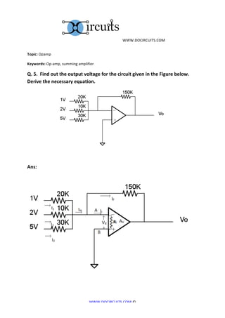
![WWW.DOCIRCUITS.COM
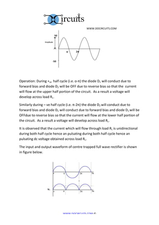
Consider
the
different
voltage
&
current
with
different
nodes
&
different
paths
as
shown
in
figure
above.
The
above
circuit
can
be
simplified
by
using
virtual
ground
concept
for
getting
its
output
voltage
VO.
As
per
virtual
ground
concept
Let
(i)
AV
=∞=Vd=0
Volt
=VA
–
VB
=
O
Volt
But
from
above
circuit
as
VB=0
volt
Hence
VA
=
0
Volt.
Again
Ri
=∞Ω.
So
Ii
=
0mAmP
Applying
KCI
at
node
A
we
can
obtain
Iin
=
IF
=I1+I2+I3=IF
=1V
–
VA
/
20K
+
2V-‐VA/10K
+
5V
–
VA/30K
=
VA-‐V0/150K
=1V/20K
+
2V/10K+5V/30K=-‐VO/150K[as
VA=0V]
=V0=-‐150K
[1V/20K
+
2V
/
10K
+
5V/30K]
=-‐
150K/20K
x
1
-‐150K/10K
x
2V
-‐150K/30K
x
5V
=-‐7.5V
–
30V
–
25V=-‐62.5
Volt
WWW.DOCIRCUITS.COM
©](https://image.slidesharecdn.com/basicelectronicssampleebook-121015132408-phpapp01/85/Electronics-Circuits-EBOOK-20-320.jpg)

The document discusses various topics in basic electronics, specifically on semiconductor diodes, transistor biasing, operational amplifiers, and clipping circuits. It includes practical problems and their solutions involving wave rectification, transistor behavior, op-amp configurations, and building clipper circuits. Additionally, it provides circuit analysis and performance parameters such as efficiency and ripple factor.


