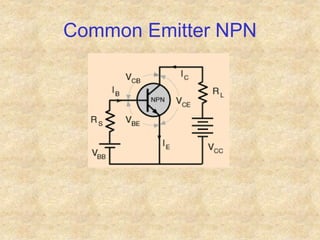
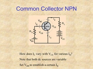
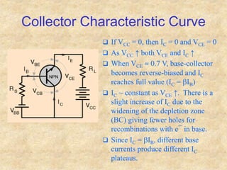
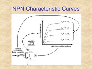
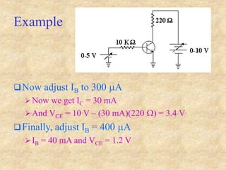
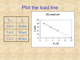
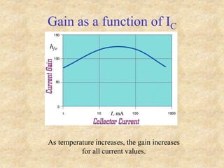
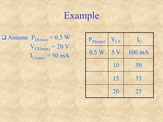
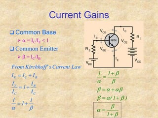
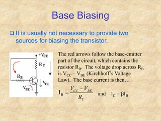
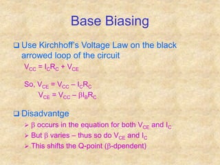
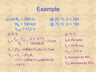
Transistors
Transfer Resistor
Chapter 9
Bipolar Transistors
Two PN junctions joined together
Two types available – NPN and PNP
The regions (from top to bottom) are called the collector (C), the
base (B), and the emitter (E)
Base
Collector
Emitter
Operation
 Begin by reverse biasing the CB junction
 Here we are showing an NPN transistor
as an example
 Now we apply a small forward bias on
the emitter-base junction
 Electrons are pushed into the base,
which then quickly flow to the collector
 The result is a large emitter-collector
electron current (conventional current is
C-E) which is maintained by a small E-B
voltage
 Some of the electrons pushed into the
base by the forward bias E-B voltage
end up depleting holes in that junction
 This would eventually destroy the
junction if we didn’t replenish the holes
 The electrons that might do this are
drawn off as a base current
Currents
Conventional View
Origin of the names
the Emitter 'emits' the electrons which
pass through the device
the Collector 'collects' them again once
they've passed through the Base
...and the Base?...
Original Manufacture
Base Thickness
 The thickness of the unmodified Base region has
to be just right.
 Too thin, and the Base would essentially vanish. The
Emitter and Collector would then form a continuous
piece of semiconductor, so current would flow
between them whatever the base potential.
 Too thick, and electrons entering the Base from the
Emitter wouldn't notice the Collector as it would be
too far away. So then, the current would all be
between the Emitter and the Base, and there'd be no
Emitter-Collector current.
Amplification Properties
The C-B voltage junction operates near
breakdown.
 This ensures that a small E-B voltage causes
avalanche
 Large current through the device
Common Base NPN
Common Emitter NPN
Common Collector NPN
How does IC vary with VCE for various IB?
Note that both dc sources are variable
Set VBB to establish a certain IB
Collector Characteristic Curve
 If VCC = 0, then IC = 0 and VCE = 0
 As VCC ↑ both VCE and IC ↑
 When VCE  0.7 V, base-collector
becomes reverse-biased and IC
reaches full value (IC = bIB)
 IC ~ constant as VCE ↑. There is a
slight increase of IC due to the
widening of the depletion zone
(BC) giving fewer holes for
recombinations with e¯ in base.
 Since IC = bIB, different base
currents produce different IC
plateaus.
NPN Characteristic Curves
PNP Characteristic Curves
Load Line
For a constant load, stepping IB gives different currents (IC) predicted by
where the load line crosses the characteristic curve. IC = bIBworks so long as
the load line intersects on the plateau region of the curve.
Slope of
the load
line is 1/RL
Saturation and Cut-off
Note that the load line intersects the 75 mA curve below the
plateau region. This is saturation and IC = bIB doesn’t work
in this region.
Cut-off
Example
We adjust the base current to 200 mA and note
that this transistor has a b = 100
 Then IC = bIB = 100(200 X 10-6A) = 20 mA
Notice that we can use Kirchhoff’s voltage law
around the right side of the circuit
 VCE = VCC – ICRC = 10 V – (20 mA)(220 W)
= 10 V – 4.4 V = 5.6 V
Example
Now adjust IB to 300 mA
 Now we get IC = 30 mA
 And VCE = 10 V – (30 mA)(220 W) = 3.4 V
Finally, adjust IB = 400 mA
 IB = 40 mA and VCE = 1.2 V
Plot the load line
VCE IC
5.6 V 20 mA
3.4 V 30 mA
1.2 V 40 mA
Gain as a function of IC
As temperature increases, the gain increases
for all current values.
Operating Limits
There will be a limit on the dissipated power
 PD(max) = VCEIC
 VCE and IC were the parameters plotted on the
characteristic curve.
 If there is a voltage limit (VCE(max)), then you can
compute the IC that results
 If there is a current limit (IC(max)), then you can compute
the VCE that results
Example
 Assume PD(max) = 0.5 W
VCE(max) = 20 V
IC(max) = 50 mA
PD(max) VCE IC
0.5 W 5 V 100 mA
10 50
15 33
20 25
Operating Range
Operating
Range
Voltage Amplifiers
Common Base PNP
Now we have added an ac source
The biasing of the junctions are:
BE is forward biased by VBB - thus a small resistance
BC is reverse biased by VCC – and a large resistance
Since IB is small, IC  IE
Equivalent ac Circuit
gain
voltage

 V
in
out
A
V
V
rE = internal ac emitter
resistance
IE = Vin/rE (Ohm’s Law)
Vout = ICRC  IERC
E
C
E
E
C
E
V
r
R
r
I
R
I
A 
 Recall the name – transfer resistor
Current Gains
 Common Base
 a = IC/IE < 1
 Common Emitter
 b = IC/IB
b
a
1
1
1
I
I
1
I
I
I
I
I
Law
Current
s
Kirchhoff'
From
C
B
C
E
B
C
E






b
b
a
b
a
b
ab
a
b
b
b
a








1
)
1
(
1
1
Example
If b = 50, then a = 50/51 = 0.98
 Recall a < 1
Rearranging,
b = a + ab
b(1-a) = a
b = a/(1-a)
Transistors as Switches
The operating points
We can control the base current using VBB (we
don’t actually use a physical switch). The circuit
then acts as a high speed switch.
Details
In Cut-off
 All currents are zero and VCE = VCC
In Saturation
 IB big enough to produce IC(sat)  bIB
Using Kirchhoff’s Voltage Law through the
ground loop
 VCC = VCE(sat) + IC(sat)RC
 but VCE(sat) is very small (few tenths), so
 IC(sat) VCC/RC
Example
a) What is VCE when Vin = 0 V?
Ans. VCE = VCC = 10 V
b) What minimum value of IB is
required to saturate the transistor if
b = 200? Take VCE(sat) = 0 V
IC(sat)  VCC/RC = 10 V/1000 W
= 10 mA
Then, IB = IC(sat)/b = 10 mA/200 = 0.05mA
Example
LED
If a square wave is input for VBB,
then the LED will be on when the
input is high, and off when the
input is low.
Transistors with ac Input
Assume that b is such that
IC varies between 20 and 40
mA. The transistor is
constantly changing curves
along the load line.
Pt. A corresponds to the positive peak. Pt. B
corresponds to the negative peak. This graph shows
ideal operation.
Distortion
The location of the point Q (size of the dc
source on input) may cause an operating
point to lie outside of the active range.
Driven to saturation
Driven into Cutoff
Base Biasing
 It is usually not necessary to provide two
sources for biasing the transistor.
The red arrows follow the base-emitter
part of the circuit, which contains the
resistor RB. The voltage drop across RB
is VCC – VBE (Kirchhoff’s Voltage
Law). The base current is then…
C
BE
CC
R
V
V 

B
I and IC = bIB
Base Biasing
 Use Kirchhoff’s Voltage Law on the black
arrowed loop of the circuit
VCC = ICRC + VCE
So, VCE = VCC – ICRC
VCE = VCC – bIBRC
 Disadvantge
 b occurs in the equation for both VCE and IC
 But b varies – thus so do VCE and IC
 This shifts the Q-point (b-dpendent)
Example
 Let RC = 560 W @ 25 °C b = 100
RB = 100 kW @ 75 °C b = 150
VCC = +12 V
mA
11.3
A)
(100)(113
I
I B
C 

 m
b
V
5.67
)
A)(560
(100)(113
-
V
12
R
I
V
V C
B
CC
CE




W
m
b
@ 75 °C
IB is the same
IC = 16.95 mA
VCE = 2.51 V
IC increases by 50%
VCE decreases by 56%
A
113
100,000
V
0.7
-
V
12
I
C
25
@
B m
W





B
BE
CC
R
V
V
Transistor Amplifiers
Amplification
 The process of increasing the strength of a
signal.
 The result of controlling a relatively large
quantity of current (output) with a small
quantity of current (input).
Amplifier
 Device use to increase the current, voltage, or
power of the input signal without appreciably
altering the essential quality.
Class A
Entire input waveform is faithfully
reproduced.
Transistor spends its entire time in the
active mode
 Never reaches either cutoff or saturation.
 Drive the transistor exactly halfway between
cutoff and saturation.
 Transistor is always on – always dissipating
power – can be quite inefficient
Class A
Class B
No DC bias voltage
 The transistor spends half its time in active
mode and the other half in cutoff
Push-pull Pair
Transistor Q1 "pushes" (drives the output voltage in a positive direction with
respect to ground), while transistor Q2 "pulls" the output voltage (in a negative
direction, toward 0 volts with respect to ground).
Individually, each of these transistors is operating in class B mode, active only for
one-half of the input waveform cycle. Together, however, they function as a team to
produce an output waveform identical in shape to the input waveform.
Class AB
Between Class A (100% operation) and
Class B (50% operation).
Class C
IC flows for less than half then cycle. Usually get
more gain in Class B and C, but more distortion
Common Emitter Transistor Amplifier
Notice that VBB forward biases the emitter-base junction and dc
current flows through the circuit at all times
The class of the amplifier is determined by VBB with respect to the
input signal.
Signal that adds to VBB causes transistor current to increase
Signal that subtracts from VBB causes transistor current to decrease
Details
 At positive peak of input, VBB is adding to the
input
 Resistance in the transistor is reduced
 Current in the circuit increases
 Larger current means more voltage drop across
RC (VRC = IRC)
 Larger voltage drop across RC leaves less
voltage to be dropped across the transistor
 We take the output VCE – as input increases, VCE
decreases.
More details
As the input goes to the negative peak
 Transistor resistance increases
 Less current flows
 Less voltage is dropped across RC
 More voltage can be dropped across C-E
The result is a phase reversal
 Feature of the common emitter amplifier
The closer VBB is to VCC, the larger the
transistor current.
PNP Common Emitter Amplifier
NPN Common Base Transistor
Amplifier
Signal that adds to VBB causes transistor current to increase
Signal that subtracts from VBB causes transistor current to decrease
• At positive peak of input, VBB is adding to the input
• Resistance in the transistor is reduced
• Current in the circuit increases
• Larger current means more voltage drop across RC (VRC = IRC)
• Collector current increases
• No phase reversal
PNP Common Base Amplifier
NPN Common Collector Transistor
Amplifier
Also called an Emitter Follower circuit – output on emitter is almost a replica of the
input
Input is across the C-B junction – this is reversed biased and the impedance is high
Output is across the B-E junction – this is forward biased and the impedance is low.
Current gain is high but voltage gain is low.
PNP Common Collector Transistor
Amplifier
Gain Factors
E
C
I
I

a Usually given for common base amplifier
B
C
I
I

b Usually given for common emitter amplifier
B
E
I
I

 Usually given for common collector amplifier
Gamma
 Recall from Kirchhoff’s Current Law
 IB + IC = IE

b
1
I
I
I
I
1
I
B
E
B
C
B





a

a
a
a

a
a
a
a
b
-
1
1
-
1
-
1
LCD
-
1
1
-
1
since
And






Ex. For b = 100 a = b/(1+b) = 0.99
 = 1 + b = 101
Bringing it Together
Type Common
Base
Common
Emitter
Common
Collector
Relation
between
input/output
phase
0° 180° 0°
Voltage Gain High Medium Low
Current Gain Low (a) Medium (b) High ()
Power Gain Low High Medium
Input Z Low Medium High
Output Z High Medium Low
Hybrid Parameters
Condition
hi Input resistance Output shorted
hr Voltage feedback ratio Input open
hf Forward current gain Output shorted
ho Output conductance Input open
Second subscript indicates common base (b), common emitter
(e), or common collector (c)
Hybrid Parameters
= b
= Slope of curve
Hybrid Parameters
hie = VB/IB Ohm’s Law
hie =input impedance
hre = VB/VC
Hybrid Parameters
hfe = IC/IB
Equivalent of b
hoe = IC/VC
Various Forms
Common
Emitter (e)
Common
Base (b)
Common
Collector (c)
hi (ohms) VB/IB VE/IB VB/IB
hr (unitless) VB/VC VE/VC VB/VE
hf (unitless) IC/IB IC/IE IE/IB
ho (watts) ICVC ICVC IEVE
Pin-outs
No standard – look at the spec sheet or the case
Loudness
 When the energy (intensity) of the sound
increases by a factor of 10, the loudness
increases by 1 bel
 Named for A. G. Bell
 One bel is a large unit and we use 1/10th bel, or
decibels
 When the energy (intensity) of the sound
increases by a factor of 10, the loudness
increases by 10 dB
Decibel Scale
For intensities
 L = 10 log(I/Io)
For energies
 L = 10 log(E/Eo)
For amplitudes
 L = 20 log(A/Ao)
Threshold of Hearing
 The Io or Eo or Ao refers to the intensity, energy, or
amplitude of the sound wave for the threshold of
hearing
 Io = 10-12 W/m2
 Loudness levels always compared to threshold
 Relative measure
Common Loud Sounds
160
Jet engine - close up
150
Snare drums played hard at 6 inches away
Trumpet peaks at 5 inches away
140 Rock singer screaming in microphone (lips on mic)
130
Pneumatic (jack) hammer Cymbal crash
Planes on airport runway 120 Threshold of pain - Piccolo strongly played
Fender guitar amplifier, full volume at 10 inches away
Power tools 110
Subway (not the sandwich shop) 100
Flute in players right ear - Violin in players left
ear
Common Quieter Sounds
90
Heavy truck traffic
Chamber music 80
Typical home stereo listening level
Acoustic guitar, played with finger at 1 foot away
Average factory
70
Busy street Small orchestra
60 Conversational speech at 1 foot away
Average office noise 50
Quiet conversation 40
Quiet office 30
Quiet living room 20
10 Quiet recording studio
0 Threshold of hearing for healthy youths
The Math
l1 = 10 log(I1/Io)
l2 = 10 log(I2/Io)
l2 – l1 = Dl = 10(log I2 – log Io – log I1 + log Io)
= 10(log I2 – log I1)
l2 – l1 = Dl = 10 log(I2/I1)
Threshold of Hearing when I = Io l = 0 dB
Threshold of Pain when I  1012 Io l = 120 dB
Example
 A loudspeaker produces loudness rated at 90 dB
(l1) at a distance of 4 ft (d1). How far can the
sound travel (d2) and still give a loudness at the
listener’s ear of 40 dB (l2 - conversation at 3 ft.)?
Sound follows the inverse square law I1/I2 = d2
2/d1
2
Dl = 50 dB = 10 log(I2/I1)
log(I2/I1) = 5 which means I2/I1 = 105
If d1 = 4 ft, then d2
2 = (I1/I2) d1
2 = 105 (4 ft)2
d2 = 1260 ft (about ¼ mile)
Common Emitter Current Gain
For the -3 dB point
 Dl = 3 dB = 10 log (I1/I2)
 I1/I2 = 2 = P1/P2
 so 3 dB below initial level mean half the power
Frequency
hfe
0 dB
-3 dB
Why do Frequency limits occur?
 It takes a certain time for e- to travel from emitter
to collector (transit time)
 If frequency is too high, applied current varies
too rapidly
 Electrons may be unable to dislodge rapidly
enough to move from E to C before current
surges in the other direction.
Making the base thinner reduces transit time and
improves frequency response
Interelement Capacitance
 As reverse bias increases on the C-B junction,
the depletion zone increases and C decreases
(C = eA/d and d increasing).
 As emitter current increases, C increases (d
decreasing).
 If capacitance changes, so does capacitive
reactance
 Increasing C decreases XC
C
f
2
1
XC


Feedback
Small base current provides a path back to
input
 If the feedback voltage aids the input voltage,
then it is positive (regenerative) feedback
 If the feedback is too large, the amplifier will
oscillate
Superheterodyne Receiver

Transistors.ppt

  • 1.
  • 2.
    Bipolar Transistors Two PNjunctions joined together Two types available – NPN and PNP The regions (from top to bottom) are called the collector (C), the base (B), and the emitter (E) Base Collector Emitter
  • 3.
    Operation  Begin byreverse biasing the CB junction  Here we are showing an NPN transistor as an example  Now we apply a small forward bias on the emitter-base junction  Electrons are pushed into the base, which then quickly flow to the collector  The result is a large emitter-collector electron current (conventional current is C-E) which is maintained by a small E-B voltage  Some of the electrons pushed into the base by the forward bias E-B voltage end up depleting holes in that junction  This would eventually destroy the junction if we didn’t replenish the holes  The electrons that might do this are drawn off as a base current
  • 4.
  • 5.
  • 6.
    Origin of thenames the Emitter 'emits' the electrons which pass through the device the Collector 'collects' them again once they've passed through the Base ...and the Base?...
  • 7.
  • 8.
    Base Thickness  Thethickness of the unmodified Base region has to be just right.  Too thin, and the Base would essentially vanish. The Emitter and Collector would then form a continuous piece of semiconductor, so current would flow between them whatever the base potential.  Too thick, and electrons entering the Base from the Emitter wouldn't notice the Collector as it would be too far away. So then, the current would all be between the Emitter and the Base, and there'd be no Emitter-Collector current.
  • 9.
    Amplification Properties The C-Bvoltage junction operates near breakdown.  This ensures that a small E-B voltage causes avalanche  Large current through the device
  • 10.
  • 11.
  • 12.
    Common Collector NPN Howdoes IC vary with VCE for various IB? Note that both dc sources are variable Set VBB to establish a certain IB
  • 13.
    Collector Characteristic Curve If VCC = 0, then IC = 0 and VCE = 0  As VCC ↑ both VCE and IC ↑  When VCE  0.7 V, base-collector becomes reverse-biased and IC reaches full value (IC = bIB)  IC ~ constant as VCE ↑. There is a slight increase of IC due to the widening of the depletion zone (BC) giving fewer holes for recombinations with e¯ in base.  Since IC = bIB, different base currents produce different IC plateaus.
  • 14.
  • 15.
  • 16.
    Load Line For aconstant load, stepping IB gives different currents (IC) predicted by where the load line crosses the characteristic curve. IC = bIBworks so long as the load line intersects on the plateau region of the curve. Slope of the load line is 1/RL
  • 17.
    Saturation and Cut-off Notethat the load line intersects the 75 mA curve below the plateau region. This is saturation and IC = bIB doesn’t work in this region. Cut-off
  • 18.
    Example We adjust thebase current to 200 mA and note that this transistor has a b = 100  Then IC = bIB = 100(200 X 10-6A) = 20 mA Notice that we can use Kirchhoff’s voltage law around the right side of the circuit  VCE = VCC – ICRC = 10 V – (20 mA)(220 W) = 10 V – 4.4 V = 5.6 V
  • 19.
    Example Now adjust IBto 300 mA  Now we get IC = 30 mA  And VCE = 10 V – (30 mA)(220 W) = 3.4 V Finally, adjust IB = 400 mA  IB = 40 mA and VCE = 1.2 V
  • 20.
    Plot the loadline VCE IC 5.6 V 20 mA 3.4 V 30 mA 1.2 V 40 mA
  • 21.
    Gain as afunction of IC As temperature increases, the gain increases for all current values.
  • 22.
    Operating Limits There willbe a limit on the dissipated power  PD(max) = VCEIC  VCE and IC were the parameters plotted on the characteristic curve.  If there is a voltage limit (VCE(max)), then you can compute the IC that results  If there is a current limit (IC(max)), then you can compute the VCE that results
  • 23.
    Example  Assume PD(max)= 0.5 W VCE(max) = 20 V IC(max) = 50 mA PD(max) VCE IC 0.5 W 5 V 100 mA 10 50 15 33 20 25
  • 24.
  • 25.
    Voltage Amplifiers Common BasePNP Now we have added an ac source The biasing of the junctions are: BE is forward biased by VBB - thus a small resistance BC is reverse biased by VCC – and a large resistance Since IB is small, IC  IE
  • 26.
    Equivalent ac Circuit gain voltage  V in out A V V rE = internal ac emitter resistance IE = Vin/rE (Ohm’s Law) Vout = ICRC  IERC E C E E C E V r R r I R I A   Recall the name – transfer resistor
  • 27.
    Current Gains  CommonBase  a = IC/IE < 1  Common Emitter  b = IC/IB b a 1 1 1 I I 1 I I I I I Law Current s Kirchhoff' From C B C E B C E       b b a b a b ab a b b b a         1 ) 1 ( 1 1
  • 28.
    Example If b =50, then a = 50/51 = 0.98  Recall a < 1 Rearranging, b = a + ab b(1-a) = a b = a/(1-a)
  • 29.
  • 30.
    The operating points Wecan control the base current using VBB (we don’t actually use a physical switch). The circuit then acts as a high speed switch.
  • 31.
    Details In Cut-off  Allcurrents are zero and VCE = VCC In Saturation  IB big enough to produce IC(sat)  bIB Using Kirchhoff’s Voltage Law through the ground loop  VCC = VCE(sat) + IC(sat)RC  but VCE(sat) is very small (few tenths), so  IC(sat) VCC/RC
  • 32.
    Example a) What isVCE when Vin = 0 V? Ans. VCE = VCC = 10 V b) What minimum value of IB is required to saturate the transistor if b = 200? Take VCE(sat) = 0 V IC(sat)  VCC/RC = 10 V/1000 W = 10 mA Then, IB = IC(sat)/b = 10 mA/200 = 0.05mA
  • 33.
    Example LED If a squarewave is input for VBB, then the LED will be on when the input is high, and off when the input is low.
  • 34.
    Transistors with acInput Assume that b is such that IC varies between 20 and 40 mA. The transistor is constantly changing curves along the load line.
  • 35.
    Pt. A correspondsto the positive peak. Pt. B corresponds to the negative peak. This graph shows ideal operation.
  • 36.
    Distortion The location ofthe point Q (size of the dc source on input) may cause an operating point to lie outside of the active range. Driven to saturation Driven into Cutoff
  • 37.
    Base Biasing  Itis usually not necessary to provide two sources for biasing the transistor. The red arrows follow the base-emitter part of the circuit, which contains the resistor RB. The voltage drop across RB is VCC – VBE (Kirchhoff’s Voltage Law). The base current is then… C BE CC R V V   B I and IC = bIB
  • 38.
    Base Biasing  UseKirchhoff’s Voltage Law on the black arrowed loop of the circuit VCC = ICRC + VCE So, VCE = VCC – ICRC VCE = VCC – bIBRC  Disadvantge  b occurs in the equation for both VCE and IC  But b varies – thus so do VCE and IC  This shifts the Q-point (b-dpendent)
  • 39.
    Example  Let RC= 560 W @ 25 °C b = 100 RB = 100 kW @ 75 °C b = 150 VCC = +12 V mA 11.3 A) (100)(113 I I B C    m b V 5.67 ) A)(560 (100)(113 - V 12 R I V V C B CC CE     W m b @ 75 °C IB is the same IC = 16.95 mA VCE = 2.51 V IC increases by 50% VCE decreases by 56% A 113 100,000 V 0.7 - V 12 I C 25 @ B m W      B BE CC R V V
  • 40.
    Transistor Amplifiers Amplification  Theprocess of increasing the strength of a signal.  The result of controlling a relatively large quantity of current (output) with a small quantity of current (input). Amplifier  Device use to increase the current, voltage, or power of the input signal without appreciably altering the essential quality.
  • 41.
    Class A Entire inputwaveform is faithfully reproduced. Transistor spends its entire time in the active mode  Never reaches either cutoff or saturation.  Drive the transistor exactly halfway between cutoff and saturation.  Transistor is always on – always dissipating power – can be quite inefficient
  • 42.
  • 43.
    Class B No DCbias voltage  The transistor spends half its time in active mode and the other half in cutoff
  • 44.
    Push-pull Pair Transistor Q1"pushes" (drives the output voltage in a positive direction with respect to ground), while transistor Q2 "pulls" the output voltage (in a negative direction, toward 0 volts with respect to ground). Individually, each of these transistors is operating in class B mode, active only for one-half of the input waveform cycle. Together, however, they function as a team to produce an output waveform identical in shape to the input waveform.
  • 45.
    Class AB Between ClassA (100% operation) and Class B (50% operation).
  • 46.
    Class C IC flowsfor less than half then cycle. Usually get more gain in Class B and C, but more distortion
  • 47.
    Common Emitter TransistorAmplifier Notice that VBB forward biases the emitter-base junction and dc current flows through the circuit at all times The class of the amplifier is determined by VBB with respect to the input signal. Signal that adds to VBB causes transistor current to increase Signal that subtracts from VBB causes transistor current to decrease
  • 48.
    Details  At positivepeak of input, VBB is adding to the input  Resistance in the transistor is reduced  Current in the circuit increases  Larger current means more voltage drop across RC (VRC = IRC)  Larger voltage drop across RC leaves less voltage to be dropped across the transistor  We take the output VCE – as input increases, VCE decreases.
  • 49.
    More details As theinput goes to the negative peak  Transistor resistance increases  Less current flows  Less voltage is dropped across RC  More voltage can be dropped across C-E The result is a phase reversal  Feature of the common emitter amplifier The closer VBB is to VCC, the larger the transistor current.
  • 50.
  • 51.
    NPN Common BaseTransistor Amplifier Signal that adds to VBB causes transistor current to increase Signal that subtracts from VBB causes transistor current to decrease • At positive peak of input, VBB is adding to the input • Resistance in the transistor is reduced • Current in the circuit increases • Larger current means more voltage drop across RC (VRC = IRC) • Collector current increases • No phase reversal
  • 52.
    PNP Common BaseAmplifier
  • 53.
    NPN Common CollectorTransistor Amplifier Also called an Emitter Follower circuit – output on emitter is almost a replica of the input Input is across the C-B junction – this is reversed biased and the impedance is high Output is across the B-E junction – this is forward biased and the impedance is low. Current gain is high but voltage gain is low.
  • 54.
    PNP Common CollectorTransistor Amplifier
  • 55.
    Gain Factors E C I I  a Usuallygiven for common base amplifier B C I I  b Usually given for common emitter amplifier B E I I   Usually given for common collector amplifier
  • 56.
    Gamma  Recall fromKirchhoff’s Current Law  IB + IC = IE  b 1 I I I I 1 I B E B C B      a  a a a  a a a a b - 1 1 - 1 - 1 LCD - 1 1 - 1 since And       Ex. For b = 100 a = b/(1+b) = 0.99  = 1 + b = 101
  • 57.
    Bringing it Together TypeCommon Base Common Emitter Common Collector Relation between input/output phase 0° 180° 0° Voltage Gain High Medium Low Current Gain Low (a) Medium (b) High () Power Gain Low High Medium Input Z Low Medium High Output Z High Medium Low
  • 58.
    Hybrid Parameters Condition hi Inputresistance Output shorted hr Voltage feedback ratio Input open hf Forward current gain Output shorted ho Output conductance Input open Second subscript indicates common base (b), common emitter (e), or common collector (c)
  • 59.
  • 60.
    Hybrid Parameters hie =VB/IB Ohm’s Law hie =input impedance hre = VB/VC
  • 61.
    Hybrid Parameters hfe =IC/IB Equivalent of b hoe = IC/VC
  • 62.
    Various Forms Common Emitter (e) Common Base(b) Common Collector (c) hi (ohms) VB/IB VE/IB VB/IB hr (unitless) VB/VC VE/VC VB/VE hf (unitless) IC/IB IC/IE IE/IB ho (watts) ICVC ICVC IEVE
  • 63.
    Pin-outs No standard –look at the spec sheet or the case
  • 64.
    Loudness  When theenergy (intensity) of the sound increases by a factor of 10, the loudness increases by 1 bel  Named for A. G. Bell  One bel is a large unit and we use 1/10th bel, or decibels  When the energy (intensity) of the sound increases by a factor of 10, the loudness increases by 10 dB
  • 65.
    Decibel Scale For intensities L = 10 log(I/Io) For energies  L = 10 log(E/Eo) For amplitudes  L = 20 log(A/Ao)
  • 66.
    Threshold of Hearing The Io or Eo or Ao refers to the intensity, energy, or amplitude of the sound wave for the threshold of hearing  Io = 10-12 W/m2  Loudness levels always compared to threshold  Relative measure
  • 67.
    Common Loud Sounds 160 Jetengine - close up 150 Snare drums played hard at 6 inches away Trumpet peaks at 5 inches away 140 Rock singer screaming in microphone (lips on mic) 130 Pneumatic (jack) hammer Cymbal crash Planes on airport runway 120 Threshold of pain - Piccolo strongly played Fender guitar amplifier, full volume at 10 inches away Power tools 110 Subway (not the sandwich shop) 100 Flute in players right ear - Violin in players left ear
  • 68.
    Common Quieter Sounds 90 Heavytruck traffic Chamber music 80 Typical home stereo listening level Acoustic guitar, played with finger at 1 foot away Average factory 70 Busy street Small orchestra 60 Conversational speech at 1 foot away Average office noise 50 Quiet conversation 40 Quiet office 30 Quiet living room 20 10 Quiet recording studio 0 Threshold of hearing for healthy youths
  • 69.
    The Math l1 =10 log(I1/Io) l2 = 10 log(I2/Io) l2 – l1 = Dl = 10(log I2 – log Io – log I1 + log Io) = 10(log I2 – log I1) l2 – l1 = Dl = 10 log(I2/I1) Threshold of Hearing when I = Io l = 0 dB Threshold of Pain when I  1012 Io l = 120 dB
  • 70.
    Example  A loudspeakerproduces loudness rated at 90 dB (l1) at a distance of 4 ft (d1). How far can the sound travel (d2) and still give a loudness at the listener’s ear of 40 dB (l2 - conversation at 3 ft.)? Sound follows the inverse square law I1/I2 = d2 2/d1 2 Dl = 50 dB = 10 log(I2/I1) log(I2/I1) = 5 which means I2/I1 = 105 If d1 = 4 ft, then d2 2 = (I1/I2) d1 2 = 105 (4 ft)2 d2 = 1260 ft (about ¼ mile)
  • 71.
    Common Emitter CurrentGain For the -3 dB point  Dl = 3 dB = 10 log (I1/I2)  I1/I2 = 2 = P1/P2  so 3 dB below initial level mean half the power Frequency hfe 0 dB -3 dB
  • 72.
    Why do Frequencylimits occur?  It takes a certain time for e- to travel from emitter to collector (transit time)  If frequency is too high, applied current varies too rapidly  Electrons may be unable to dislodge rapidly enough to move from E to C before current surges in the other direction. Making the base thinner reduces transit time and improves frequency response
  • 73.
    Interelement Capacitance  Asreverse bias increases on the C-B junction, the depletion zone increases and C decreases (C = eA/d and d increasing).  As emitter current increases, C increases (d decreasing).  If capacitance changes, so does capacitive reactance  Increasing C decreases XC C f 2 1 XC  
  • 74.
    Feedback Small base currentprovides a path back to input  If the feedback voltage aids the input voltage, then it is positive (regenerative) feedback  If the feedback is too large, the amplifier will oscillate
  • 75.