Downloaded 845 times


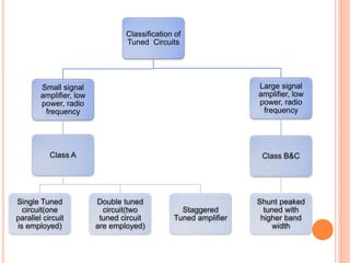


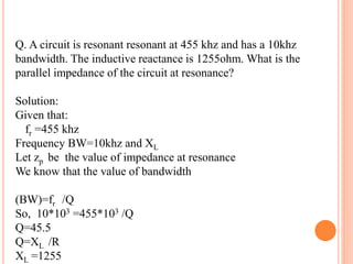
![Since at resonance
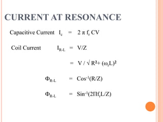
Reactive component of coil current = Capacitive current
(V / Z ) * (2 π frL / Z) = 2 π frCV
Z = √(L/C) ………..(1)
Line current IL = Active component of coil current
= IA
= IR-L cosФR-L
= VR/Z2 [using (1)]
= VR(C/L)
IL = [ V / (L/RC) ]
(L/RC) = Effective or equivalent dynamic impedance of
parallel circuit at resonance.](https://image.slidesharecdn.com/tunedamplifire-151021095624-lva1-app6891/85/Tuned-amplifire-32-320.jpg)

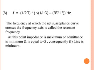


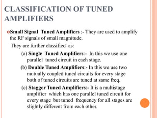
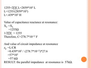
![We know:
Resonant frequency = 1/ 2 π √[ (1/LC) – (R2 / L2 ) ]
= 1 / 2 π √[(1/10*10-3 - 25/100*10-6)
]
= 5.034 KHz
Q = 2 π * 5.034 * 10-3 * 10 * 10-3 / 5
= 63.227
BW = FR /Q = 5.034 / 63.227
= 79.62KHz
RESULT:- Fr = 5.034 KHz
Q = 63.227
BW = 79.62KHz](https://image.slidesharecdn.com/tunedamplifire-151021095624-lva1-app6891/85/Tuned-amplifire-66-320.jpg)


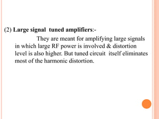
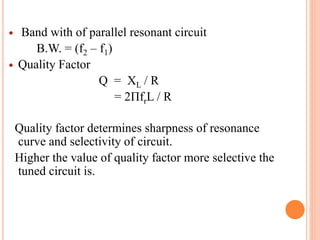
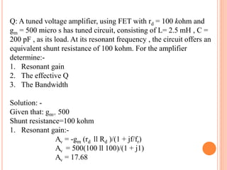
![Rac = Rp ll RL
Rp = Qdc * XL
= 10.205 * 408.2
= 4165.681
RL = 4* 106
Rac = 4161.34
Qac = [Rac / XL ]
= 4161.34/408.2
= 10.194
Result: -
Fr = 1.3 MHz
Qdc = 10.205
Qac = 10.194](https://image.slidesharecdn.com/tunedamplifire-151021095624-lva1-app6891/85/Tuned-amplifire-69-320.jpg)


The document provides a comprehensive overview of tuned amplifiers, detailing their functionality, characteristics, and classifications including single, double, and stagger tuned amplifiers. It explains the principles of resonance in various circuit configurations, such as series and parallel resonant circuits, and discusses applications for low and large signal amplifiers. Additionally, it highlights the advantages and disadvantages of tuned amplifiers in communication systems and includes numerical examples to demonstrate calculations related to resonance frequency, quality factor, and bandwidth.


