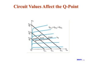
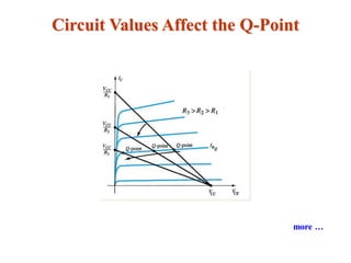
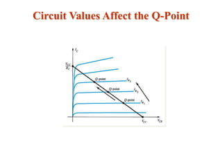
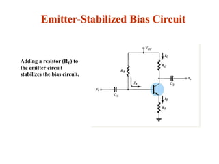
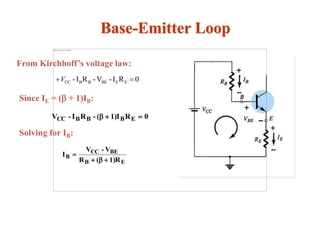
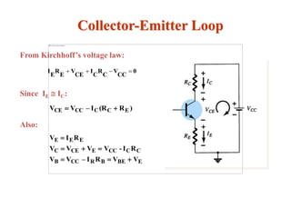
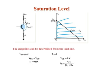
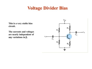
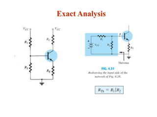
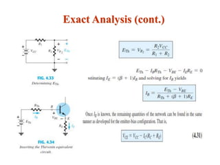
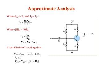
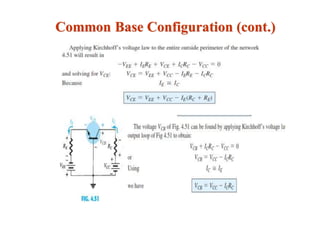
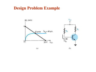
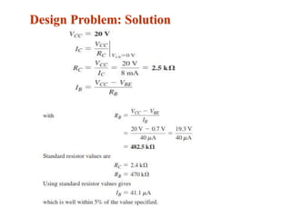
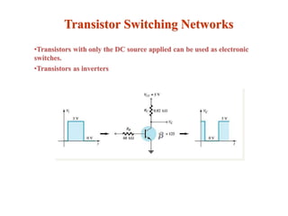
This document discusses integrated circuits and operational amplifiers. It provides information on the classification, advantages and development of integrated circuits over time, moving from small-scale to large-scale integration. It also details the characteristics, symbols, configurations and applications of operational amplifiers, including inverting, non-inverting and voltage follower circuits. Operational amplifiers can be used in both open and closed loop modes, with closed loop preferred for linear applications due to negative feedback controlling gain.
1. A multivibrator can implement simple two-state systems like oscillators, timers, and flip-flops. There are three types: astable which oscillates between states, monostable which is stable in one state until triggered to the other, and bistable which remains in either state.
2. An astable multivibrator consists of two amplifying devices cross-coupled by resistors and capacitors that cause it to continuously oscillate between two states.
3. A monostable multivibrator is stable in one state until an external trigger briefly changes its state, after which it returns to the original stable state for a set time period, functioning as a timer.
The document provides information about bipolar junction transistors (BJTs), including:
1) BJTs have three doped semiconductor regions (emitter, base, collector) separated by two pn junctions and operate using both holes and electrons.
2) For a BJT to operate as an amplifier, the base-emitter junction must be forward-biased and the base-collector junction must be reverse-biased.
3) Changes in base current cause much larger changes in collector current, allowing BJTs to amplify signals.
This document discusses different biasing techniques for MOSFETs, including biasing with a feedback resistor and voltage divider bias. It provides the equations to calculate the drain current, drain-source voltage, and gate voltage for each biasing method. It also discusses an example problem calculating the current, voltage, and power dissipation for a common-source MOSFET circuit. Thermal stability of transistors is briefly covered as well.
Bipolar junction transistors (BJTs) are three-terminal semiconductor devices consisting of two pn junctions. There are two types, NPN and PNP, depending on the order of doping. BJTs can operate as amplifiers and switches by controlling the flow of majority charge carriers through the base terminal. Proper biasing is required to operate the transistor in its active region between cutoff and saturation. Common configurations include common-base, common-emitter, and common-collector, each with different input and output characteristics. Maximum ratings like power dissipation and voltages must be considered for circuit design and temperature derating.
Diodes and its application encapsulate the different characteristics of different type of diodes. Also, define its different biases and how it works.
It provides shortcut method in analyzing Clamper and clipper.
At the end of the powerpoint, there has a review question to answer with answer key provided.
The document discusses Field Effect Transistors (FETs). It begins by defining some key characteristics of FETs, including that they are unipolar devices controlled by voltage and have very high input impedance. It then describes different types of FETs, including JFETs, MOSFETs, and discusses their characteristics such as transfer curves. The document provides examples of biasing circuits used for FETs and analyzing FET amplifiers at mid-frequency.
This document discusses nodal analysis, a technique for analyzing electrical circuits where the voltages at different nodes of the circuit are calculated. It provides examples of applying Kirchhoff's Current Law (KCL) and Kirchhoff's Voltage Law (KVL) to set up equations relating the currents and voltages in a circuit containing resistors connected in a mesh. The document explains how to use these equations to solve for the unknown voltages at each node of the circuit.
The document outlines the key topics in a presentation on bipolar junction transistors, including:
- The formation of NPN and PNP junctions and the operation of NPN transistors.
- The three transistor circuit configurations - common base, common emitter, and common collector - and their current gain characteristics.
- Expressions for collector current and concepts like reverse saturation current and ICEO.
- Static characteristics like input and output characteristics are examined for each configuration.
The document presents information on MOSFET operation and characteristics. It discusses that MOSFETs are widely used in electronics as switches and for auto intensity control of street lights. It describes the basic construction of MOSFETs, noting they have an insulating layer of SiO2 and a polysilicon gate. The two main types of MOSFETs are introduced as enhancement type and depletion type. Key characteristics of enhancement type MOSFETs are described, including that drain current increases with increasing gate-source voltage above a threshold.
This document contains two numerical problems involving BJT transistors. The first problem calculates alpha and emitter current given collector current, leakage current, and the percentage of carriers crossing the collector-base junction. The second problem calculates various currents and voltages for a fixed bias circuit given beta and VBE, including IB, IC, VCE, VB, VC, and VBC. The document is authored by Dr. Piyush Charan of Integral University and licensed for open use.
There are four main methods of transistor biasing: base resistor method, emitter bias method, biasing with collector feedback resistor, and voltage-divider bias method. The document then focuses on explaining the base resistor method and voltage-divider bias method in more detail. For the base resistor method, a resistor is used to provide base current, but it has poor stability. For the voltage-divider bias method, two resistors are used to provide stable biasing of the transistor by controlling the base-emitter voltage. This method is widely used due to its stability from the emitter resistor preventing changes in collector current.
A MOSFET is a semiconductor device that can amplify or switch electronic signals. It has three terminals - drain, source, and gate. Depending on whether the semiconductor material between the drain and source is n-type or p-type, a MOSFET can be an n-channel or p-channel type. Applying a positive voltage to the gate of an n-channel MOSFET or a negative voltage to the gate of a p-channel MOSFET allows current to flow between the drain and source. MOSFETs are commonly used as switches in digital circuits like processors and as amplifiers in analog circuits. They are also used in memory devices, power supplies, and other electronic applications.
Rec101 unit ii (part 2) bjt biasing and re modelDr Naim R Kidwai
This document discusses biasing of bipolar junction transistors (BJTs) including different biasing configurations such as fixed bias, emitter bias, voltage divider bias, and collector feedback. It explains how setting the operating or quiescent point on the transistor characteristics curve is important for proper amplification. The concepts of cutoff, saturation and active regions are covered. Equations for analyzing common emitter, common base and common collector configurations are provided. An example calculation of the collector current and voltage at the operating point is shown. Finally, bias stability and factors affecting it are briefly discussed.
A bipolar junction transistor (BJT) consists of two PN junctions formed by sandwiching either a p-type or n-type semiconductor between two opposite types. It has three sections - the emitter, base, and collector. Current flows due to both electrons and holes, making it a bipolar device. The base is lightly doped and very thin to allow charge carriers to easily move from the emitter to the collector. BJTs can be used as amplifiers because the collector current is controlled by the base current.
Bipolar Junction Transistor (BJT) DC and AC AnalysisJess Rangcasajo
BJT AC and DC Analysis
This slide condenses the two ways analysis of BJT (AC and DC).
At the end of the slide, it has review question answer with answer key as providing.
This document provides information about two-port network parameters including Z, Y, H, and ABCD parameters. It defines a two-port network as having two ports for input and output with two terminals pairs. The document explains that the parameters relate the terminal voltages and currents and can be determined by setting the input or output port to open or short circuit conditions. Examples are given to show how to calculate the parameters for simple circuits. Key points are summarized in less than 3 sentences.
1. The document discusses oscillators and feedback amplifiers. It explains that in feedback amplifiers, the gain and phase shift changes with frequency which can cause positive feedback and oscillations.
2. For a system to be stable, all poles and zeros of the transfer function must lie in the left half of the complex plane. The Nyquist diagram is used to check stability by plotting gain and phase shift versus frequency.
3. An oscillator converts DC power into AC oscillations of a desired frequency through positive feedback. The tank circuit determines the frequency. Barkhausen criteria must be satisfied for oscillations.
Power amplifiers are concerned with efficiency, maximum power capability, and impedance matching to the output device rather than small-signal factors like amplification, linearity, and gain. There are several classes of power amplifiers including Class A, B, AB, C, and D which differ based on the conduction angle of the output and location of the Q-point. Efficiency increases as the conduction angle decreases from Class A to Class B to Class C. Transformers can be used to improve efficiency and increase the output swing of Class A amplifiers. Push-pull configurations are used for Class B amplifiers to generate a full output cycle from two transistors.
DC biasing applies fixed voltages to transistors to place them in an operating region for amplification. The operating point defines the transistor's quiescent operating conditions under DC. Stability refers to a circuit's insensitivity to parameter variations like temperature. Emitter-stabilized and voltage divider biasing improve stability over fixed biasing by incorporating an emitter or voltage divider resistor. Feedback biasing further increases stability by introducing negative feedback from collector to base.
Field-effect transistor amplifiers provide an excellent voltage gain with the added feature of high input impedance. They are also low-power-consumption configurations with good frequency range and minimal size and weight.
JFETs, depletion MOSFETs, and MESFETs can be used to design amplifiers having similar voltage gains.
The depletion MOSFET (MESFET) circuit, however, has a much higher input impedance than a similar JFET configuration.
The document discusses bipolar junction transistors (BJTs). It describes the basic construction of an NPN and PNP transistor including the emitter, base, and collector regions. It explains that the base-emitter junction must be forward biased and the base-collector junction must be reverse biased for the transistor to operate properly. The document also discusses BJT biasing circuits, operating regions including cutoff, saturation, and active modes, and uses of BJTs as switches and amplifiers.
This document discusses the common collector (CC) transistor configuration. In a CC configuration, the base is the input, the emitter is the output, and the collector is common to both. It has a voltage gain slightly less than unity. The CC configuration has different input and output characteristics compared to common base and common emitter. It is useful for impedance matching between circuits and as a "buffer" to keep the output voltage constant over a range when driving a load.
Introduction
Band Pass Amplifiers
Series & Parallel Resonant Circuits & their Bandwidth
Analysis of Single Tuned Amplifiers
Analysis of Double Tuned Amplifiers
Primary & Secondary Tuned Amplifiers with BJT & FET
Merits and de-merits of Tuned Amplifiers
An oscillator is an electronic circuit that produces repetitive waveforms without an external input signal. It uses positive feedback to sustain oscillations, with the frequency determined by circuit components like inductors and capacitors. Common types include sinusoidal oscillators that produce sine waves, and relaxation oscillators that produce non-sinusoidal waves like square waves. Oscillators are essential components in many electronic devices and systems to generate stable frequency signals.
A cascade amplifier is a multistage amplifier circuit where each stage's output is connected to the next stage's input. This allows the total gain to be calculated as the product of the individual stage gains, greatly increasing the overall gain. Cascade amplifiers are widely used as their multistage design improves the signal strength. Key features include coupling signals between stages while blocking DC voltages, and using the output of each stage to feed the input of the next. The total gain is equal to the product of gains of each individual stage.
BJT Biasing for B.Tech Ist Year EngineeringRaghav Bansal
Okay, let's solve this step-by-step:
1) Given: IC = 2 mA
2) We're told IC = βIB
3) So we can set up and solve for β:
IC = βIB
2 mA = βIB
β = IC/IB = 2 mA / 0.5 mA = 4
So the answer for part a is:
β = 4
4) We're also given: IB = 0.5 mA
5) Using the voltage divider formula:
VB = VCC * (RB2 / (RB1 + RB2))
6) We know: VB = 0.7 V (for the B-
DC Biasing – Bipolar Junction Transistors (BJTs)ssuserb29892
This document discusses various methods of biasing bipolar junction transistors (BJTs) for proper operation, including voltage-divider bias, emitter bias, and collector feedback bias. It explains that transistors must be biased to establish a stable operating point between cutoff and saturation. Various bias circuits are analyzed using Kirchhoff's laws and the transistor model. Key aspects of establishing bias, such as determining the quiescent point and load lines, as well as sources of instability and techniques to improve stability, are covered. Examples are provided to illustrate calculating important bias parameters.
This document discusses DC and AC load lines in transistor amplifiers. It covers:
1) How DC biasing circuits set the quiescent point (Q-point) on the transistor's characteristic curve.
2) How the DC load line represents possible combinations of collector current and collector-emitter voltage.
3) How the Q-point and AC load line determine the amplifier's maximum output compliance or voltage swing.
4) How to calculate compliance using the equations related to cutoff voltage and saturation current.
This document discusses biasing circuits for BJTs. It begins by explaining that biasing circuits apply DC voltages to establish fixed operating points for transistors. This allows them to operate in the linear region. It then discusses several common biasing circuits: fixed bias, emitter-stabilized bias, and voltage divider bias. The fixed bias circuit uses two resistors and provides DC paths. The emitter-stabilized bias adds a resistor at the emitter for improved stability. The voltage divider bias uses a voltage divider network to provide DC voltages, making the operating point largely independent of transistor beta. It analyzes examples of each circuit type and discusses how to determine key voltages and currents like the Q-point, VCE, and
discussing differences faithful and un- faithful amplification
discussing stabilition in transistors
and how temperature affect collector current
discussing various methods of transistor biasing like
Base resister method ,Emitter Base method , Biasing with collector feedback method , Voltage divider bias
This document discusses transistor biasing circuits. It outlines different types of biasing circuits including fixed bias, emitter bias, collector feedback bias, and voltage divider bias. It explains how each circuit works, analyzing key parameters like collector current, collector-emitter voltage, and stability factor. The goal of biasing circuits is to set the transistor's operating point in the active region for faithful signal amplification while stabilizing it against temperature and other variations. Voltage divider bias is highlighted as the most widely used method due to its ability to stabilize the operating point through negative feedback.
Transistors can be used as switches or amplifiers. The document discusses the basics of bipolar transistors including their structure, operation, and different configurations (common base, common emitter, common collector). It provides examples of calculating currents and voltages in transistor circuits using characteristics curves and explains how different classes of amplifiers (A, B, AB, C) determine the portion of the input signal cycle during which the transistor is active.
This document contains review questions and practice problems related to transistor (BJT) circuit analysis. The review questions cover topics like current gains, transistor biasing, I-V characteristics, and transistor operation. The practice problems involve calculating operating points, currents, and voltages in common emitter amplifier circuits using transistor parameters like current gain β and bias voltages. Solving the problems requires applying concepts like Kirchhoff's laws and transistor modeling.
This document discusses Bipolar Junction Transistors (BJTs) and their operating regions. It describes the basic components and operation of NPN and PNP BJTs. The three main operating regions for BJTs are discussed: active, cutoff, and saturation regions. Equations for calculating operating points in the active region are provided. The document also discusses biasing techniques, including using a four-resistor network to provide stable biasing and prevent variations in the operating point due to changes in transistor characteristics. An example calculation of bias points is included.
This document discusses DC and AC load lines in transistor amplifiers. It covers DC biasing circuits, the voltage divider bias configuration, graphical DC bias analysis using load lines, determining the Q-point, AC equivalent circuits, AC load lines, and calculating amplifier compliance. Key points are that the DC load line shows all possible IC and VCE combinations, the Q-point is their intersection, and the AC load line determines the amplifier's maximum output voltage swing or compliance.
EST 130, Transistor Biasing and Amplification.CKSunith1
The attached narrated power point presentation explains the need for biasing in transistor amplifiers and the different biasing arrangements used in transistor circuits. The material will be useful for KTU first year B Tech students who prepare for the subject EST 130, Part B, Basic Electronics Engineering.
Biasing is the process of applying external voltages to transistors to ensure proper operation. It involves forward or reverse biasing transistor junctions to place the device in specific regions like active, saturation, or cutoff. Common biasing circuits include fixed bias using a base resistor, collector-to-base bias which provides feedback, and emitter bias where a resistor is added to stabilize operating point. Proper biasing establishes a quiescent point and load line on the transistor characteristics curve for linear amplification.
Transistors are semiconductor devices with three terminals - collector, base, and emitter. There are two main types, NPN and PNP, which differ in the doping of the semiconductor regions. Bipolar transistors can operate as amplifiers, switches, or oscillators depending on the biasing conditions. The common emitter configuration provides voltage gain but inverts the phase, while common base and common collector configurations do not invert phase. Transistor gain is determined by factors like current gain (beta) and varies based on operating point and temperature.
This chapter discusses small-signal modeling and linear amplification using transistors. The goals are to understand transistors as linear amplifiers, small-signal models, and amplifier characteristics. A simple common-emitter BJT amplifier circuit is presented and analyzed using DC and AC equivalent circuits. Key points include defining the Q-point, constructing small-signal models, and calculating voltage gain. Capacitor selection criteria are provided to maintain linearity in the amplifier.
1) CE amplifiers use bias circuits to set an operating point for the transistor. Simple bias circuits vary with transistor parameters like beta.
2) Load line analysis graphs the interplay between circuit constraints and the transistor output characteristic to determine the operating point.
3) Stabilized bias circuits aim to fix the emitter current independently of beta using an emitter resistor and potential divider bias network. Negative feedback bias circuits also use feedback from the collector voltage.
The document discusses different methods of DC biasing BJTs, including fixed bias, voltage divider bias, and emitter bias circuits. It explains how to analyze each circuit by examining the base-emitter and collector-emitter loops. The operating point (Q-point) is determined by the intersection of the transistor's output characteristics curve and the load line defined by the circuit. Adding an emitter resistor improves stability by making the Q-point less dependent on variations in the transistor's beta. Examples are provided to demonstrate how to calculate biasing voltages, currents, and the Q-point for different biasing circuits.
This document provides an overview of bipolar junction transistors (BJT) including:
- The basic structure of an NPN or PNP transistor with emitter, base, and collector layers.
- How transistors operate in cutoff, saturation, and active modes depending on biasing of the PN junctions.
- How a small base current controls a larger collector current in the active region, allowing transistors to function as electronic switches or amplifiers.
1) Bipolar junction transistors (BJTs) are commonly used semiconductor devices that can be used as amplifiers and logic switches. They consist of three terminals: collector, base, and emitter.
2) There are several types of biasing circuits that can be used with BJTs, including fixed bias, collector feedback bias, fixed bias with emitter resistor, and voltage divider biasing. Biasing circuits ensure that the BJT operates in its active region.
3) The characteristics curves of different biasing circuits show how voltages and currents vary with each other. Mathematical equations can be derived to describe the relationships between voltages and currents for different biasing configurations.
Bipolar junction transistor characterstics biassing and amplification, lab 9kehali Haileselassie
This document summarizes an experiment on characterizing the input and output properties of a bipolar junction transistor (BJT) and demonstrating its signal amplification capabilities. The experiment involved establishing the transistor's DC operating point, then evaluating its small-signal AC operation. Key results included measuring the transistor's DC current gain and small-signal voltage gain, which compared reasonably well to theoretical predictions. The document also discussed the different regions of BJT operation and their implications for circuit applications.
Bipolar junction transistor characterstics biassing and amplification, lab 9kehali Haileselassie
This document summarizes an experiment on characterizing the input and output properties of a bipolar junction transistor (BJT) and demonstrating its ability to amplify signals when biased in the active region. Key findings include:
1) Measured voltages and currents matched predicted values closely, both from hand calculations and PSPICE simulations.
2) In the active region, a small AC input signal produced a larger AC output signal, demonstrating amplification. Measured gains matched predictions from an equivalent circuit model.
3) BJT regions of interest - active, cutoff, and saturation - were explored. In the active region the BJT acts as a current source, enabling its use as a signal amplifier.
Similar to Electronics 1 : Chapter # 05 : DC Biasing BJT (20)
Electronics 1: Chapter # 01 : Electric Circuit analysis ReviewSk_Group
This document provides information about an electronics course including prerequisites, textbooks, and lecture topics. The course covers semiconductor devices, diode circuits, bipolar junction transistors, BJT amplifiers, field-effect transistors, and electric circuit analysis review. The circuit analysis review covers basic circuit elements including voltage and current sources, resistors, inductors, and capacitors. It also reviews Ohm's law, Kirchhoff's current and voltage laws, and Thevenin's and Norton's theorems. The course consists of 30 lectures covering topics like diodes, transistors, amplifiers, and analysis methods.
Batteries -Introduction – Types of Batteries – discharging and charging of battery - characteristics of battery –battery rating- various tests on battery- – Primary battery: silver button cell- Secondary battery :Ni-Cd battery-modern battery: lithium ion battery-maintenance of batteries-choices of batteries for electric vehicle applications.
Fuel Cells: Introduction- importance and classification of fuel cells - description, principle, components, applications of fuel cells: H2-O2 fuel cell, alkaline fuel cell, molten carbonate fuel cell and direct methanol fuel cells.
DEEP LEARNING FOR SMART GRID INTRUSION DETECTION: A HYBRID CNN-LSTM-BASED MODELgerogepatton
As digital technology becomes more deeply embedded in power systems, protecting the communication
networks of Smart Grids (SG) has emerged as a critical concern. Distributed Network Protocol 3 (DNP3)
represents a multi-tiered application layer protocol extensively utilized in Supervisory Control and Data
Acquisition (SCADA)-based smart grids to facilitate real-time data gathering and control functionalities.
Robust Intrusion Detection Systems (IDS) are necessary for early threat detection and mitigation because
of the interconnection of these networks, which makes them vulnerable to a variety of cyberattacks. To
solve this issue, this paper develops a hybrid Deep Learning (DL) model specifically designed for intrusion
detection in smart grids. The proposed approach is a combination of the Convolutional Neural Network
(CNN) and the Long-Short-Term Memory algorithms (LSTM). We employed a recent intrusion detection
dataset (DNP3), which focuses on unauthorized commands and Denial of Service (DoS) cyberattacks, to
train and test our model. The results of our experiments show that our CNN-LSTM method is much better
at finding smart grid intrusions than other deep learning algorithms used for classification. In addition,
our proposed approach improves accuracy, precision, recall, and F1 score, achieving a high detection
accuracy rate of 99.50%.
Advanced control scheme of doubly fed induction generator for wind turbine us...IJECEIAES
This paper describes a speed control device for generating electrical energy on an electricity network based on the doubly fed induction generator (DFIG) used for wind power conversion systems. At first, a double-fed induction generator model was constructed. A control law is formulated to govern the flow of energy between the stator of a DFIG and the energy network using three types of controllers: proportional integral (PI), sliding mode controller (SMC) and second order sliding mode controller (SOSMC). Their different results in terms of power reference tracking, reaction to unexpected speed fluctuations, sensitivity to perturbations, and resilience against machine parameter alterations are compared. MATLAB/Simulink was used to conduct the simulations for the preceding study. Multiple simulations have shown very satisfying results, and the investigations demonstrate the efficacy and power-enhancing capabilities of the suggested control system.
Harnessing WebAssembly for Real-time Stateless Streaming PipelinesChristina Lin
Traditionally, dealing with real-time data pipelines has involved significant overhead, even for straightforward tasks like data transformation or masking. However, in this talk, we’ll venture into the dynamic realm of WebAssembly (WASM) and discover how it can revolutionize the creation of stateless streaming pipelines within a Kafka (Redpanda) broker. These pipelines are adept at managing low-latency, high-data-volume scenarios.
ACEP Magazine edition 4th launched on 05.06.2024Rahul
This document provides information about the third edition of the magazine "Sthapatya" published by the Association of Civil Engineers (Practicing) Aurangabad. It includes messages from current and past presidents of ACEP, memories and photos from past ACEP events, information on life time achievement awards given by ACEP, and a technical article on concrete maintenance, repairs and strengthening. The document highlights activities of ACEP and provides a technical educational article for members.
KuberTENes Birthday Bash Guadalajara - K8sGPT first impressionsVictor Morales
K8sGPT is a tool that analyzes and diagnoses Kubernetes clusters. This presentation was used to share the requirements and dependencies to deploy K8sGPT in a local environment.
A SYSTEMATIC RISK ASSESSMENT APPROACH FOR SECURING THE SMART IRRIGATION SYSTEMSIJNSA Journal
The smart irrigation system represents an innovative approach to optimize water usage in agricultural and landscaping practices. The integration of cutting-edge technologies, including sensors, actuators, and data analysis, empowers this system to provide accurate monitoring and control of irrigation processes by leveraging real-time environmental conditions. The main objective of a smart irrigation system is to optimize water efficiency, minimize expenses, and foster the adoption of sustainable water management methods. This paper conducts a systematic risk assessment by exploring the key components/assets and their functionalities in the smart irrigation system. The crucial role of sensors in gathering data on soil moisture, weather patterns, and plant well-being is emphasized in this system. These sensors enable intelligent decision-making in irrigation scheduling and water distribution, leading to enhanced water efficiency and sustainable water management practices. Actuators enable automated control of irrigation devices, ensuring precise and targeted water delivery to plants. Additionally, the paper addresses the potential threat and vulnerabilities associated with smart irrigation systems. It discusses limitations of the system, such as power constraints and computational capabilities, and calculates the potential security risks. The paper suggests possible risk treatment methods for effective secure system operation. In conclusion, the paper emphasizes the significant benefits of implementing smart irrigation systems, including improved water conservation, increased crop yield, and reduced environmental impact. Additionally, based on the security analysis conducted, the paper recommends the implementation of countermeasures and security approaches to address vulnerabilities and ensure the integrity and reliability of the system. By incorporating these measures, smart irrigation technology can revolutionize water management practices in agriculture, promoting sustainability, resource efficiency, and safeguarding against potential security threats.
Using recycled concrete aggregates (RCA) for pavements is crucial to achieving sustainability. Implementing RCA for new pavement can minimize carbon footprint, conserve natural resources, reduce harmful emissions, and lower life cycle costs. Compared to natural aggregate (NA), RCA pavement has fewer comprehensive studies and sustainability assessments.
2. Biasing
Biasing: The DC voltages applied to a transistor in order to turn it on so
that it can amplify the AC signal.
3. Operating Point
The DC input establishes an
operating or quiescent point
called the Q-point.
4. The Three States of Operation
• Active or Linear Region Operation
Base–Emitter junction is forward biased
Base–Collector junction is reverse biased
• Cutoff Region Operation
Base–Emitter junction is reverse biased
• Saturation Region Operation
Base–Emitter junction is forward biased
Base–Collector junction is forward biased
5. DC Biasing Circuits
• Fixed-bias circuit
• Emitter-stabilized bias circuit
• Voltage divider bias circuit
• DC bias with voltage feedback
• Emitter Follower configuration
• Common base configuration
9. Transistor Saturation
When the transistor is operating in saturation, current through the transistor
is at its maximum possible value.
CR
CCV
CsatI
V0CEV
10. Load Line Analysis
ICsat
IC = VCC / RC
VCE = 0 V
VCEcutoff
VCE = VCC
IC = 0 mA
• where the value of RB sets the value of
IB
• that sets the values of VCE and IC
The Q-point is the operating point:
The end points of the load line are:
15. Base-Emitter Loop
From Kirchhoff’s voltage law:
0R1)I(-RI-V EBBBCC
0RI-V-RI- EEBEBBCC V
EB
BECC
B
1)R(R
V-V
I
Since IE = ( + 1)IB:
Solving for IB:
16. Collector-Emitter Loop
From Kirchhoff’s voltage law:
0
CC
V
C
R
C
I
CE
V
E
R
E
I
Since IE IC:
)R(RI–VV ECCCCCE
Also:
EBEBRCCB
CCCCECEC
EEE
VVRI–VV
RI-VVVV
RIV
17. Improved Biased Stability
Stability refers to a circuit condition in which the currents and voltages
will remain fairly constant over a wide range of temperatures and
transistor Beta () values.
Adding RE to the emitter improves the stability of a transistor.
22. Approximate Analysis
Where IB << I1 and I1 I2 :
Where RE > 10R2:
From Kirchhoff’s voltage law:
21
CC2
B
RR
VR
V
E
E
E
R
V
I
BEBE VVV
EECCCCCE RIRIVV
)R(RIVV
II
ECCCCCE
CE
23. Voltage Divider Bias Analysis
Transistor Saturation Level
EC
CC
CmaxCsat
RR
V
II
Load Line Analysis
Cutoff: Saturation:
mA0I
VV
C
CCCE
V0VCE
ERCR
CCV
CI
24. DC Bias with Voltage Feedback/ Collector
Feedback Configuration
Another way to
improve the stability
of a bias circuit is to
add a feedback path
from collector to
base.
In this bias circuit
the Q-point is only
slightly dependent on
the transistor beta, .
38. Switching Time
Transistor switching times:
dron ttt
fsoff ttt
Rise time 10% to 90%rt
dt
ft
st
Delay time
Storage time
Fall time 90% to 10%
39. PNP Transistors
The analysis for pnp transistor biasing circuits is the same
as that for npn transistor circuits. The only difference is that
the currents are flowing in the opposite direction.
41. Troubleshooting Hints
• Approximate voltages
– VBE .7 V for silicon transistors
– VCE 25% to 75% of VCC
• Test for opens and shorts with an ohmmeter.
• Test the solder joints.
• Test the transistor with a transistor tester or a curve tracer.
• Note that the load or the next stage affects the transistor operation.