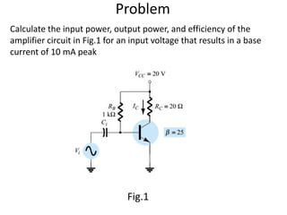
This document discusses Class A power amplifiers. Key points:
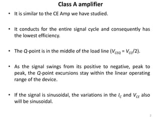
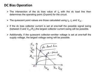
- Class A amplifiers conduct for the entire signal cycle, resulting in the lowest efficiency. The quiescent point is in the middle of the load line.
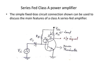
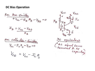
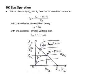
- A series fed Class A power amplifier uses a fixed bias circuit to set the operating point. The dc bias current and voltage determine the quiescent point.
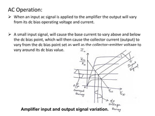
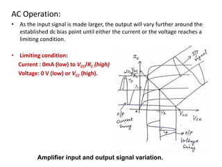
- In AC operation, an input signal causes the output to vary above and below the quiescent point. The output swings until current or voltage limits are reached.
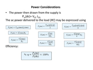
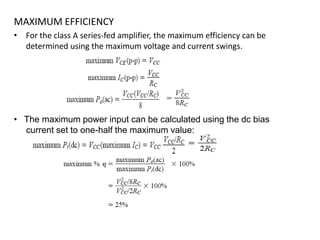
Maximum efficiency can be calculated using the maximum possible voltage and current swings given the supply voltage and load resistance. An example problem calculates input power