Download to read offline
![Design of Speed Optimized Analog to Digital Converter using VHDL
www.iosrjournals.org 42 | Page
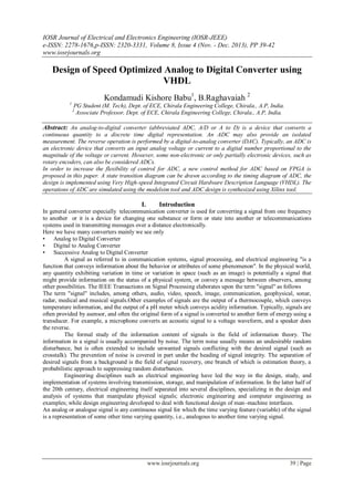
Track & Hold
A sample-and-hold (S/H) or track-and-hold (T/H) circuit is frequently required to capture rapidly
varying signals for subsequent processing by slower circuitry. The function of the S/H circuit is to
track/sample the analog input signal and to hold that value while subsequent circuitry digitizes it. Although an
S/H refers to a device which spends an infinitesimal time acquiring signals and a T/H refers to a device which
spends a finite time in this mode, common practice will be followed and the two terms will be used
interchangeably throughout this discussion as will the terms sample and track.
The function of a track-and-hold circuit is to buffer its input signal accurately during track mode
providing at its output a signal which is linearly proportional to the input, and to maintain a constant output level
during hold mode equal to the T/H output value at the instant it was strobed from track to hold by an external
clock signal. Fig. 4 shows the waveforms of a practical sample-and-hold circuit.
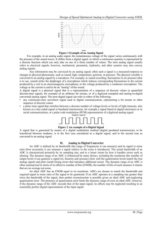
Figure 5 ADC Simulation Waveform
IV. Conclusions
Xilinx and Modelsim softwares includes a simulator which can be used to simulate the behavior and
performance of circuits designed for implementation in programmable logic devices. The simulator allows the
user to apply test vectors as inputs to the designed circuit and to observe the outputs generated in response. In
addition to being able to observe the simulated values on the I/O pins of the circuit, it is also possible to probe
the internal nodes in the circuit. The simulator makes use of the Waveform Editor, which makes it easy to
represent the desired signals as waveforms. According to the results of simulation, a new control method for
ADC is achieved. Advantages of this new method are simple programming method for high Clock frequency.
Acknowledgements
The authors would like to thank the anonymous reviewers for their comments which were very helpful
in improving the quality and presentation of this paper.
References:
[1] Petouris M (Petouris, M.), Kalantzopoulos A (Kalantzopoulos, A.),Zigouris E (Zigouris, E.), “An FPGA-based Digital Camera
System Controlled from an LCD Touch Panel” INTERNATIONAL SYMPOSIUM ON SIGNALS, CIRCUITS AND SYSTEMS,
pp. 241- 244, 2009.
[2] El-Medany, W.M. ; Hussain, M.R, “A FPGA-based advanced real traffic light controller system design” 007 4th IEEE Workshop
on Intelligent Data Acquisition and Advanced Computing Systems: Technology and Applications, IDAACS, pp. 100-105, 2007.
[3] Guo, Jianmin, Zhang, Ke, Kong, Ming, Li, Wenhong, “Novel ADC architecture for digital voltage regulator module controllers,”
Pan Tao Ti Hsueh Pao/Chinese Journal of Semiconductors, v 27, n 12, p 2112-2117,December 2006
[4] Hussein, Aziza I. ,Gruenbacher, Don M.; Ibrahim, Noureddin M , “Design and verification techniques used in a graduate level
VHDLcourse,” Proceedings - Frontiers in Education Conference, v 2, p 13a4-28 - 13a4-31, 1999.
Authors Profile:
Kondamudi Kishore Babu is Pursuing his M. Tech from Chirala Engineering College, Chirala in
the department of Electronics & Communications Engineering (ECE) with specialization in VLSI
& Embedded systems.
B.RAGHAVAIAH is working as an Associate Professor in the department of Electronics &
Communication Engineering in Chirala Engineering College, Chirala. He has completed masters
from JNTUK. He has over 8 years of teaching experience.](https://image.slidesharecdn.com/e0843942-140508020055-phpapp01/85/Design-of-Speed-Optimized-Analog-to-Digital-Converter-using-VHDL-4-320.jpg)

This document describes the design of a speed optimized analog-to-digital converter (ADC) using VHDL. It begins with background on ADCs and their components. A state transition diagram is drawn based on the ADC timing diagram and implemented in VHDL. The design is simulated using ModelSim and synthesized using Xilinx tools. Simulation waveforms show the ADC operating correctly. The new control method allows for higher clock frequencies and simpler programming compared to previous designs.


