Downloaded 910 times
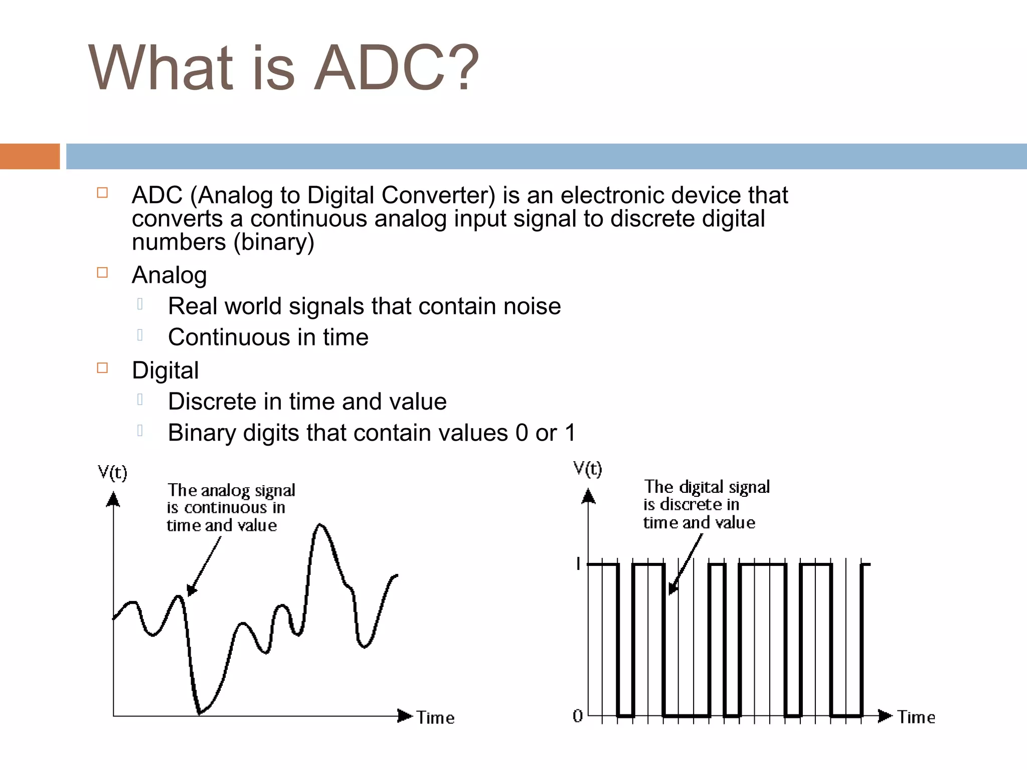
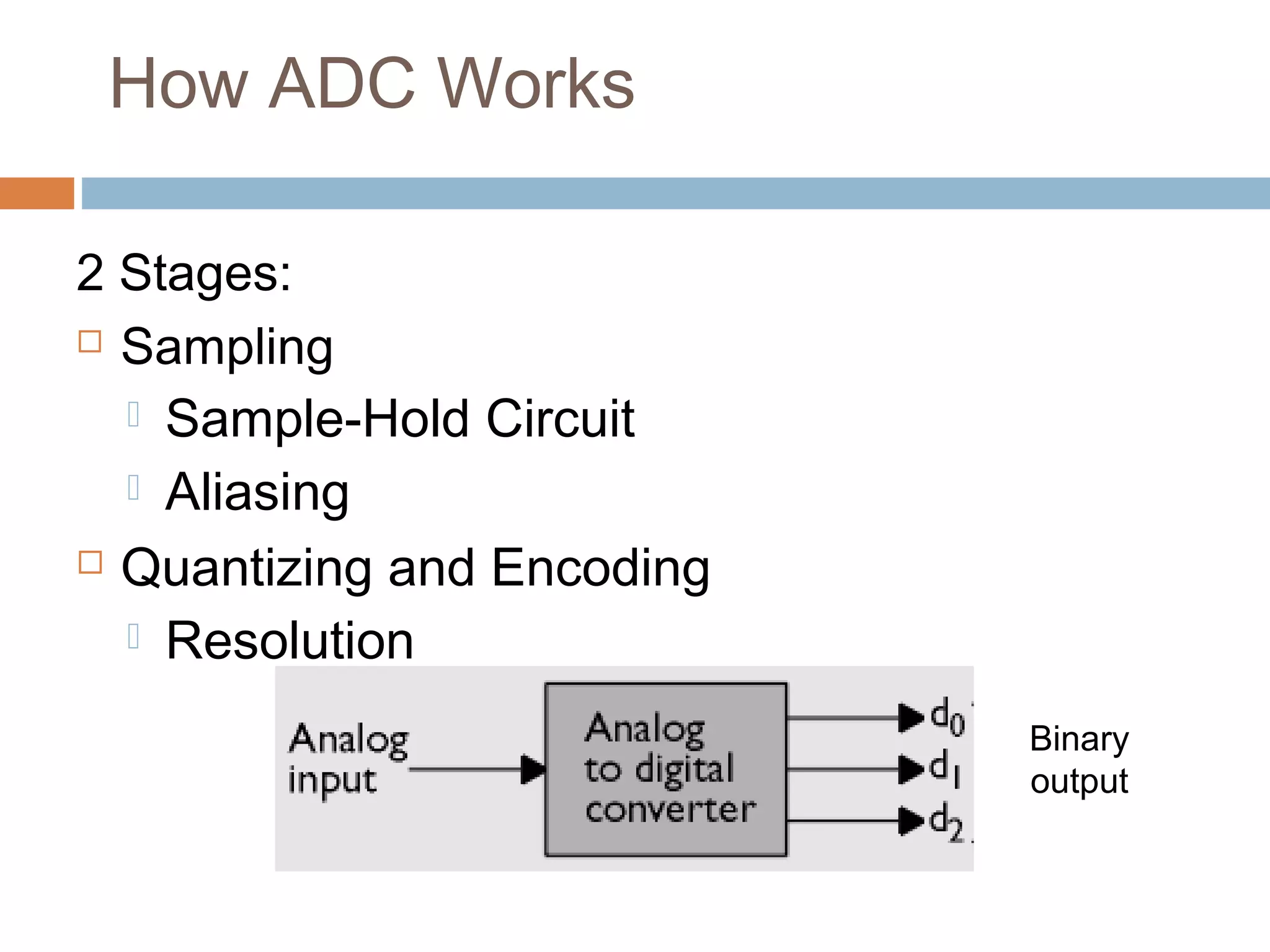
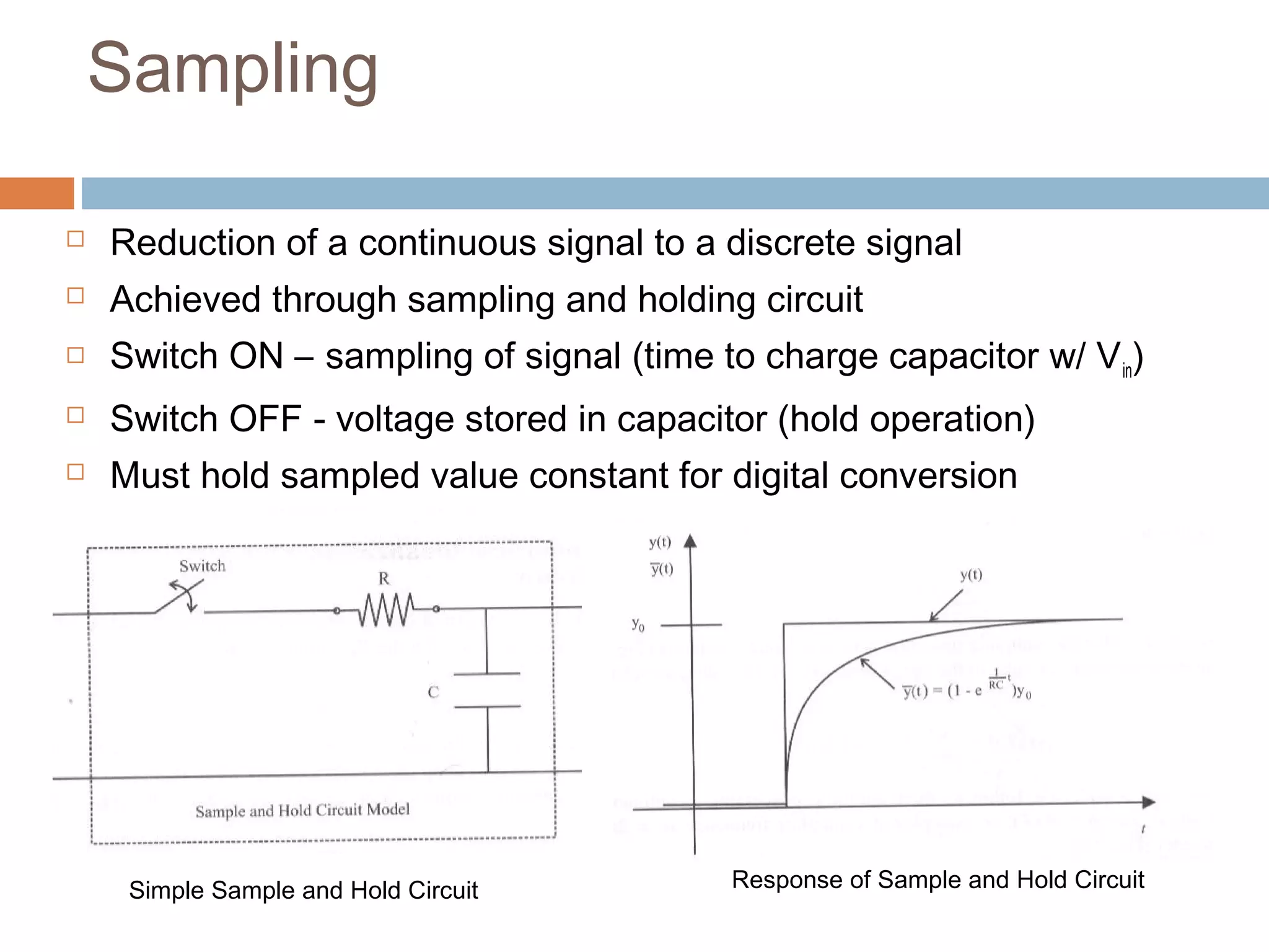
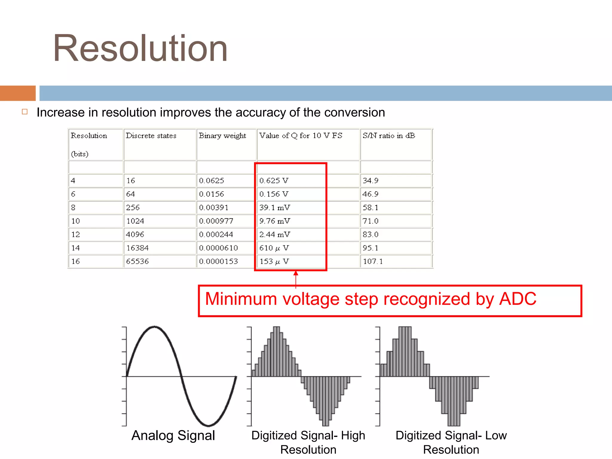
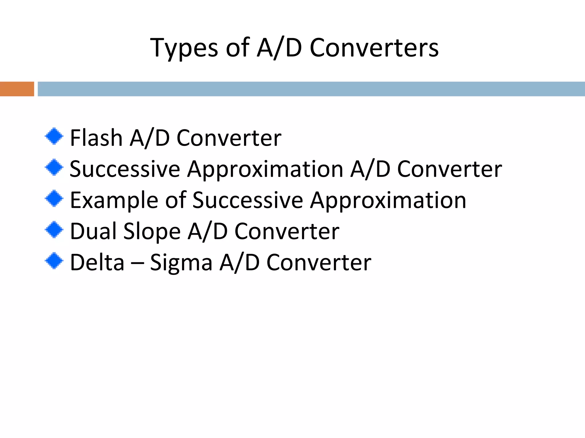
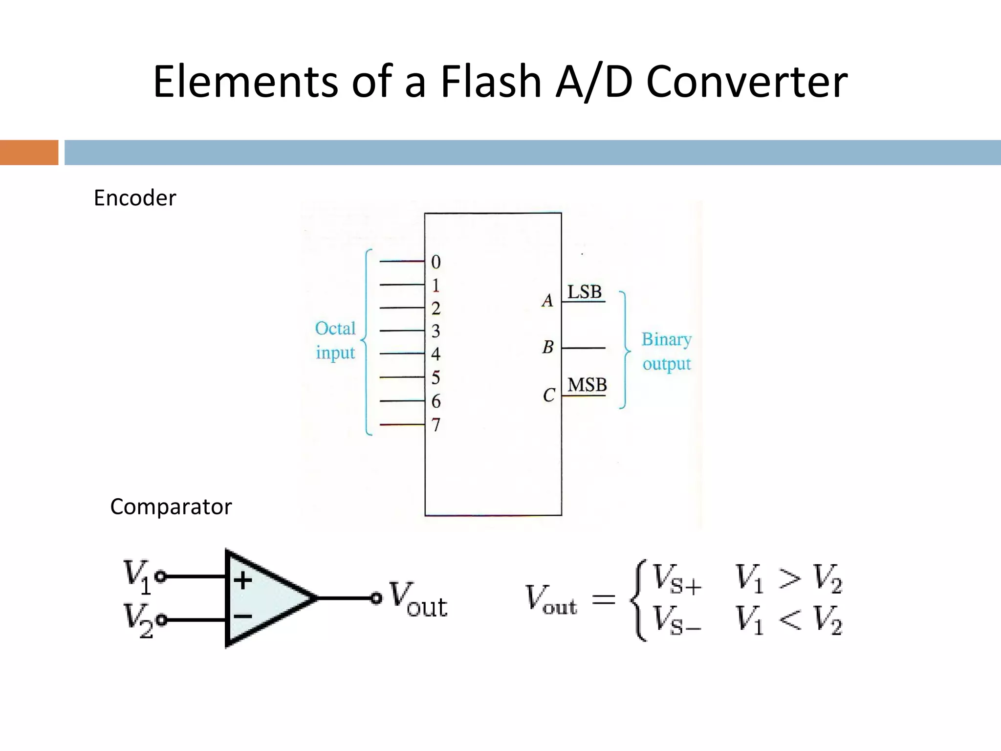
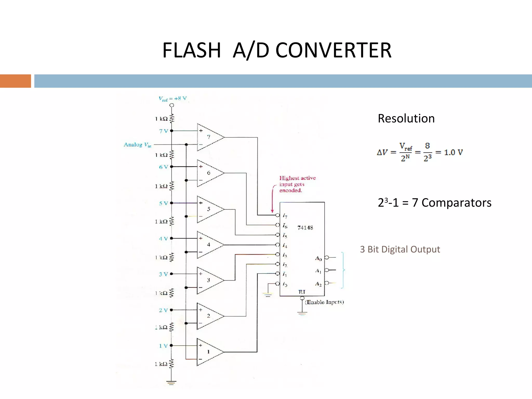
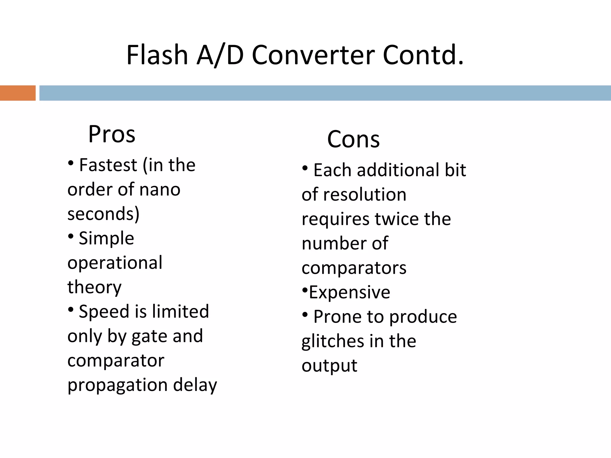
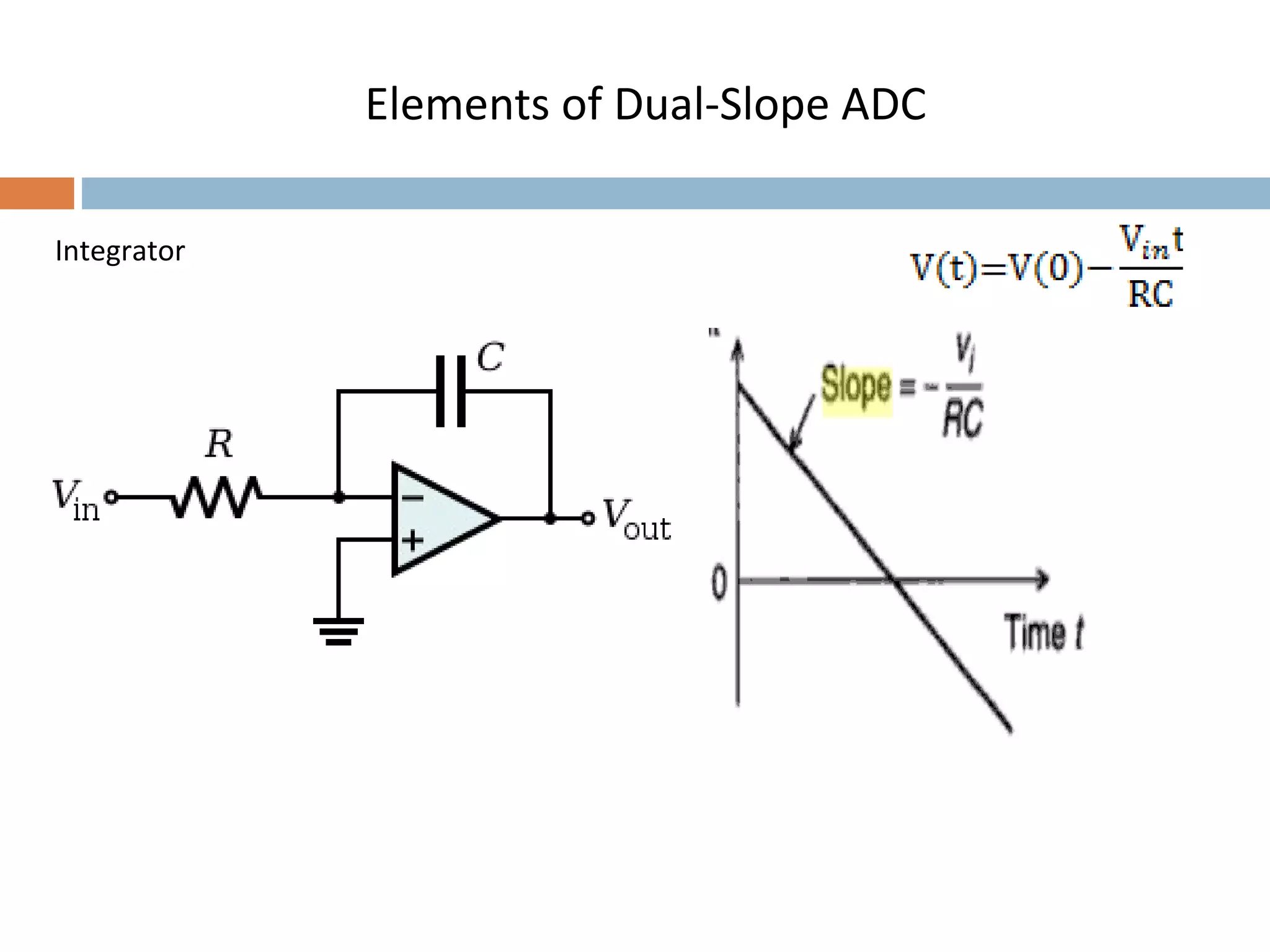
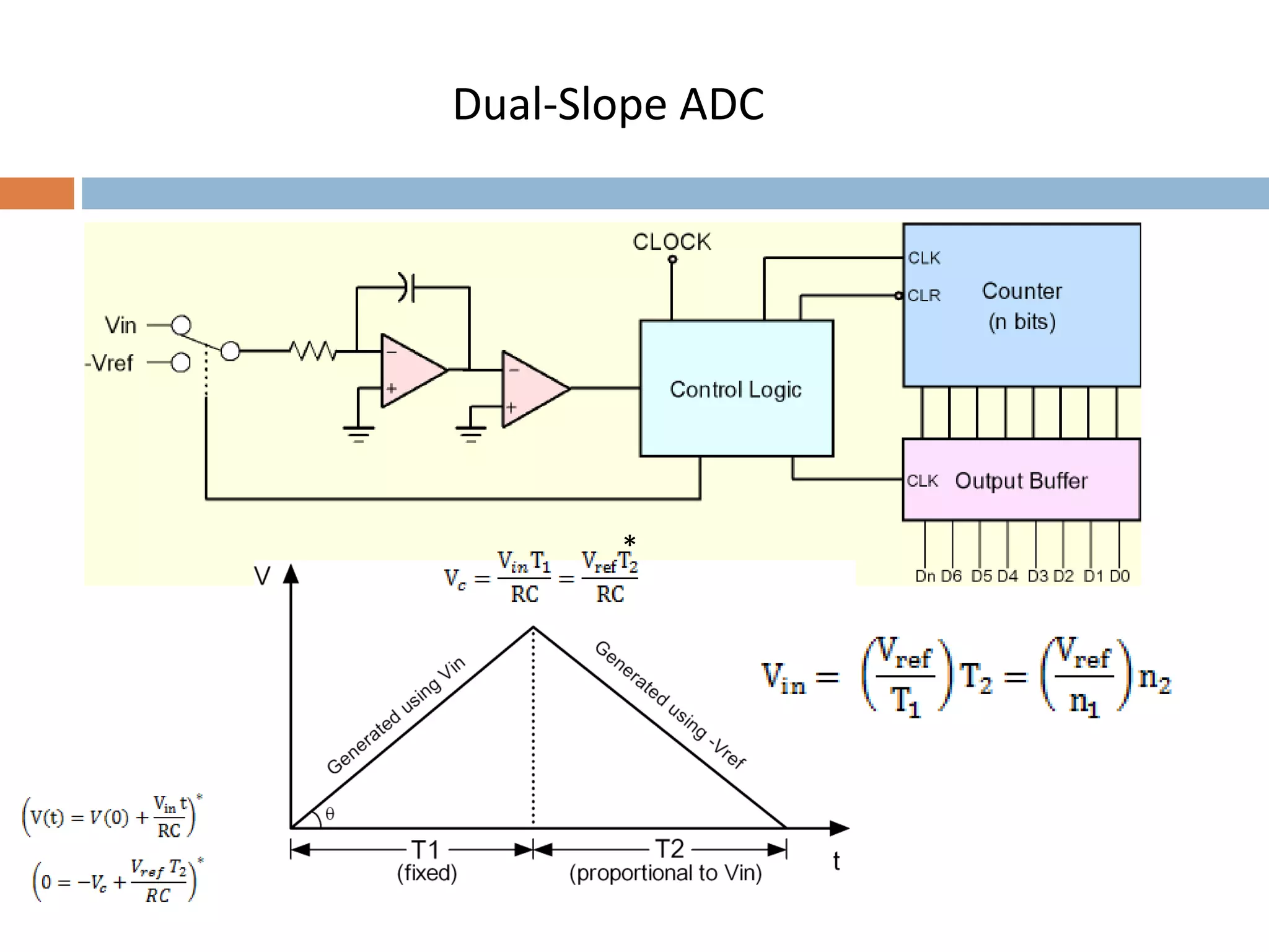
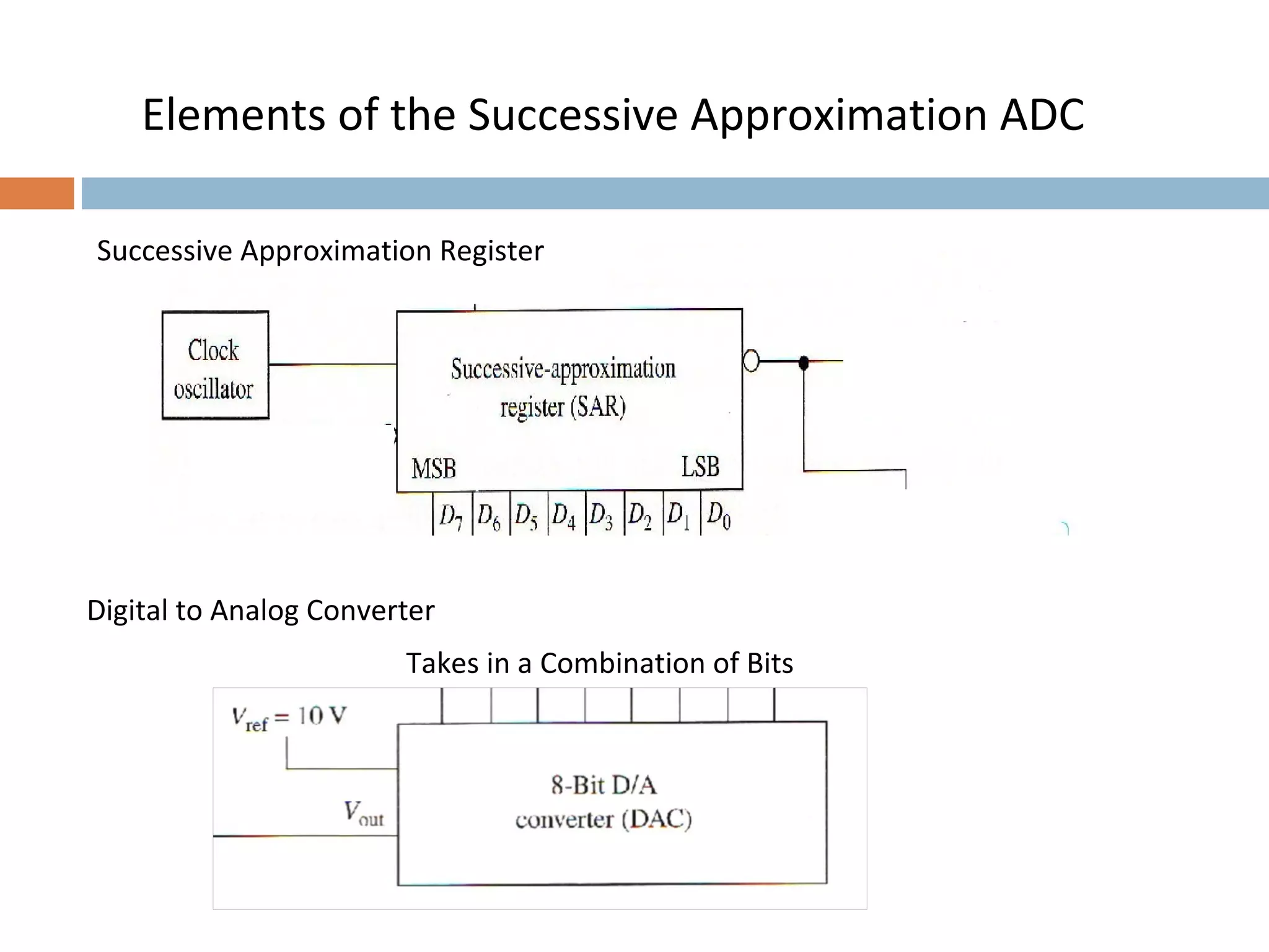
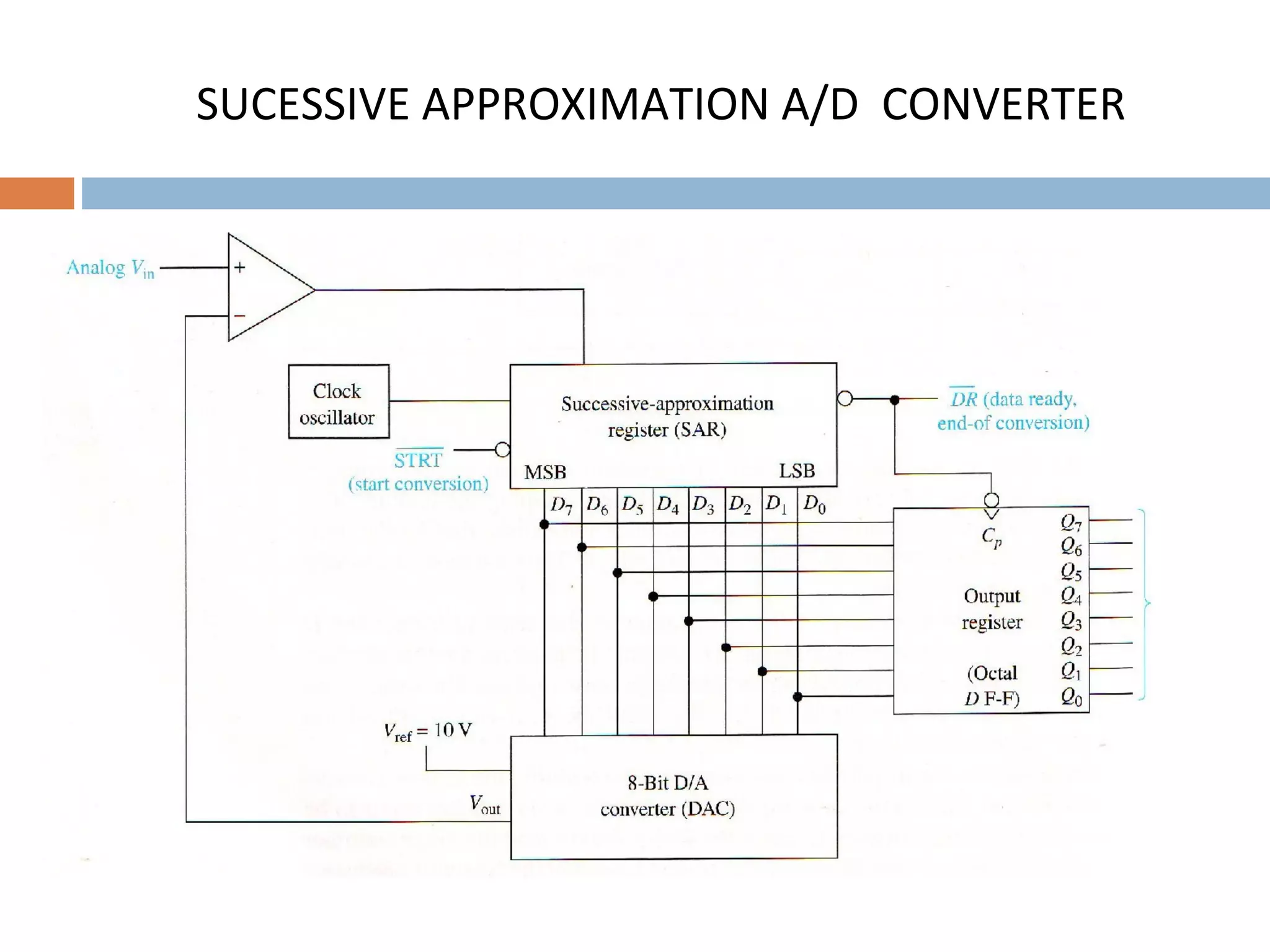
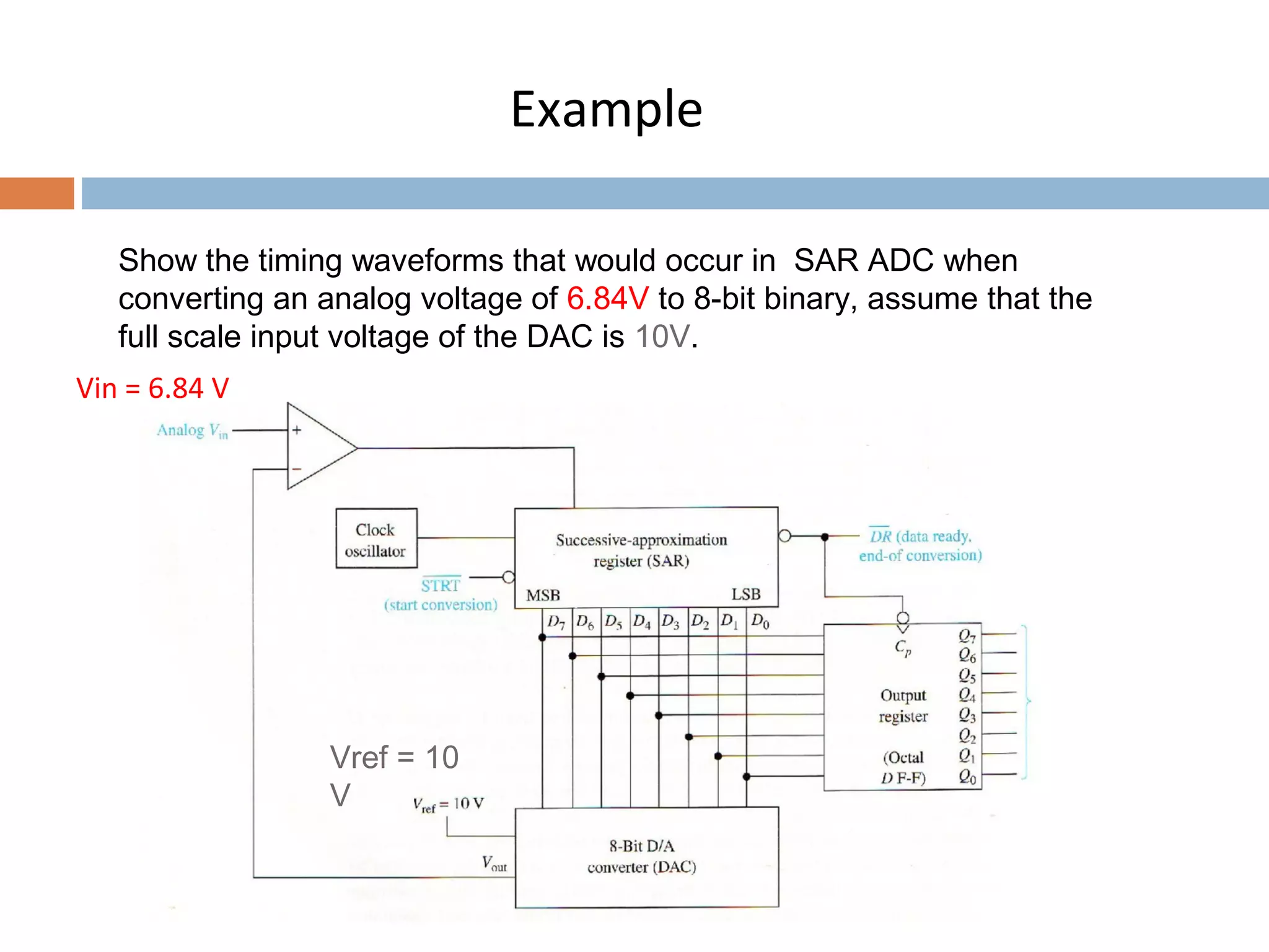
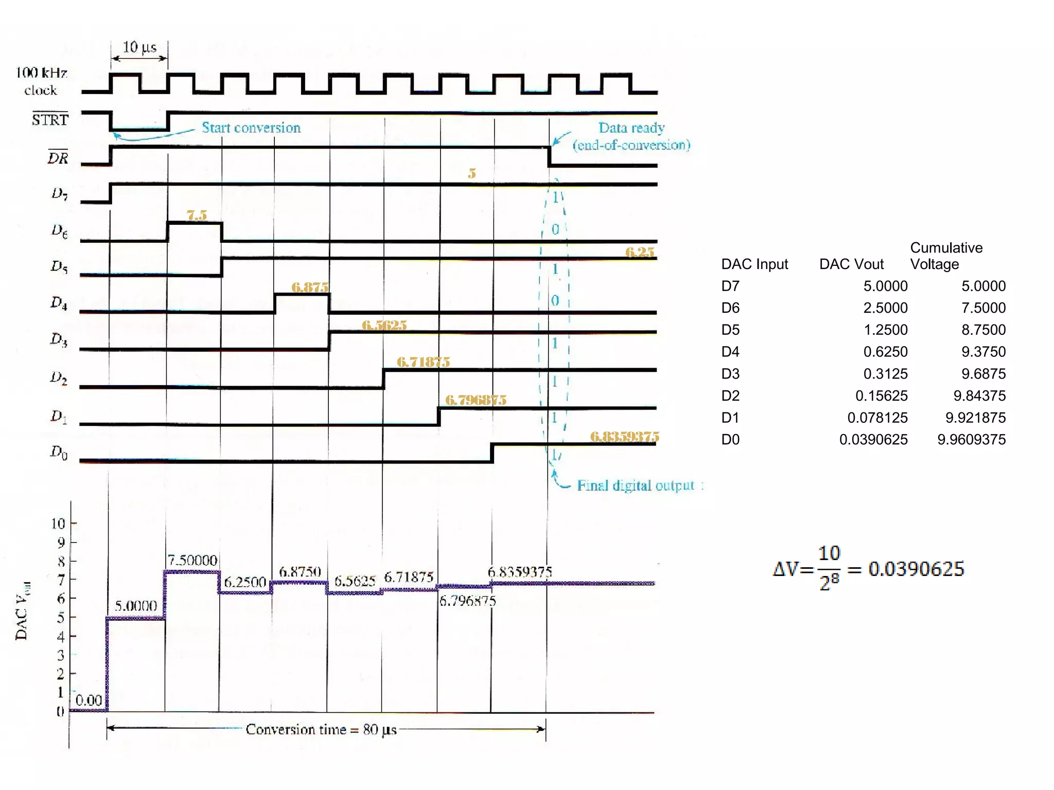
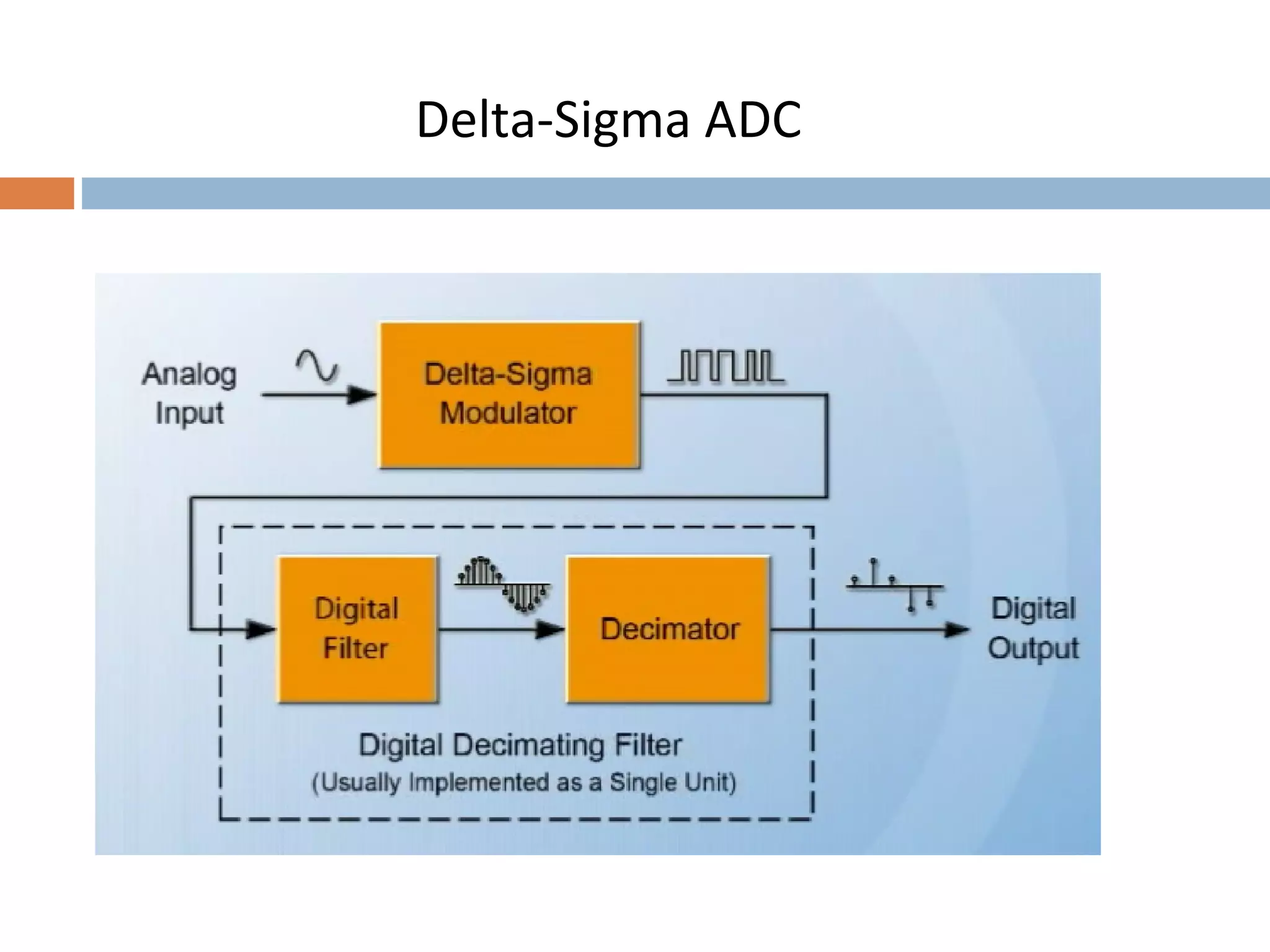

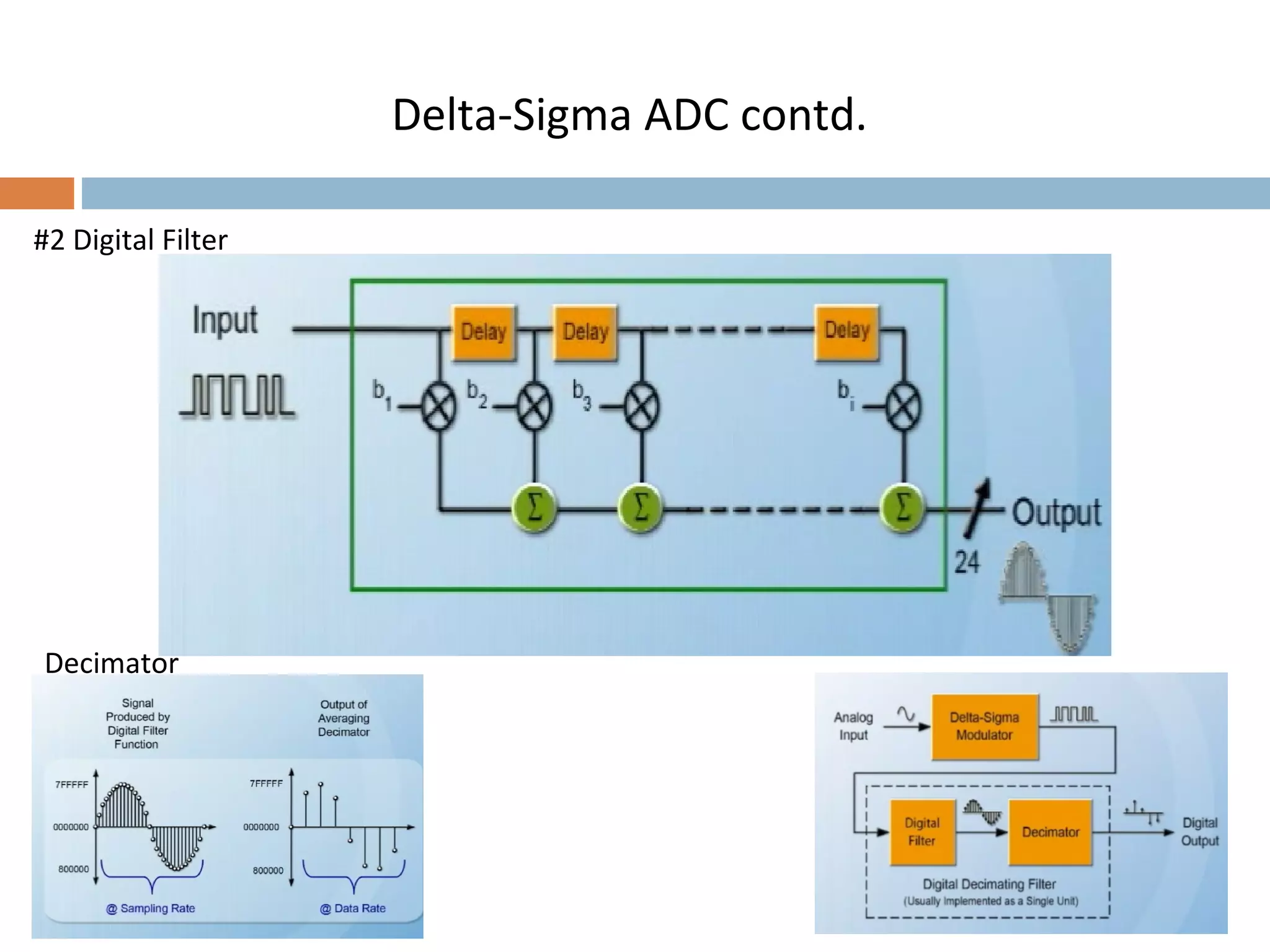
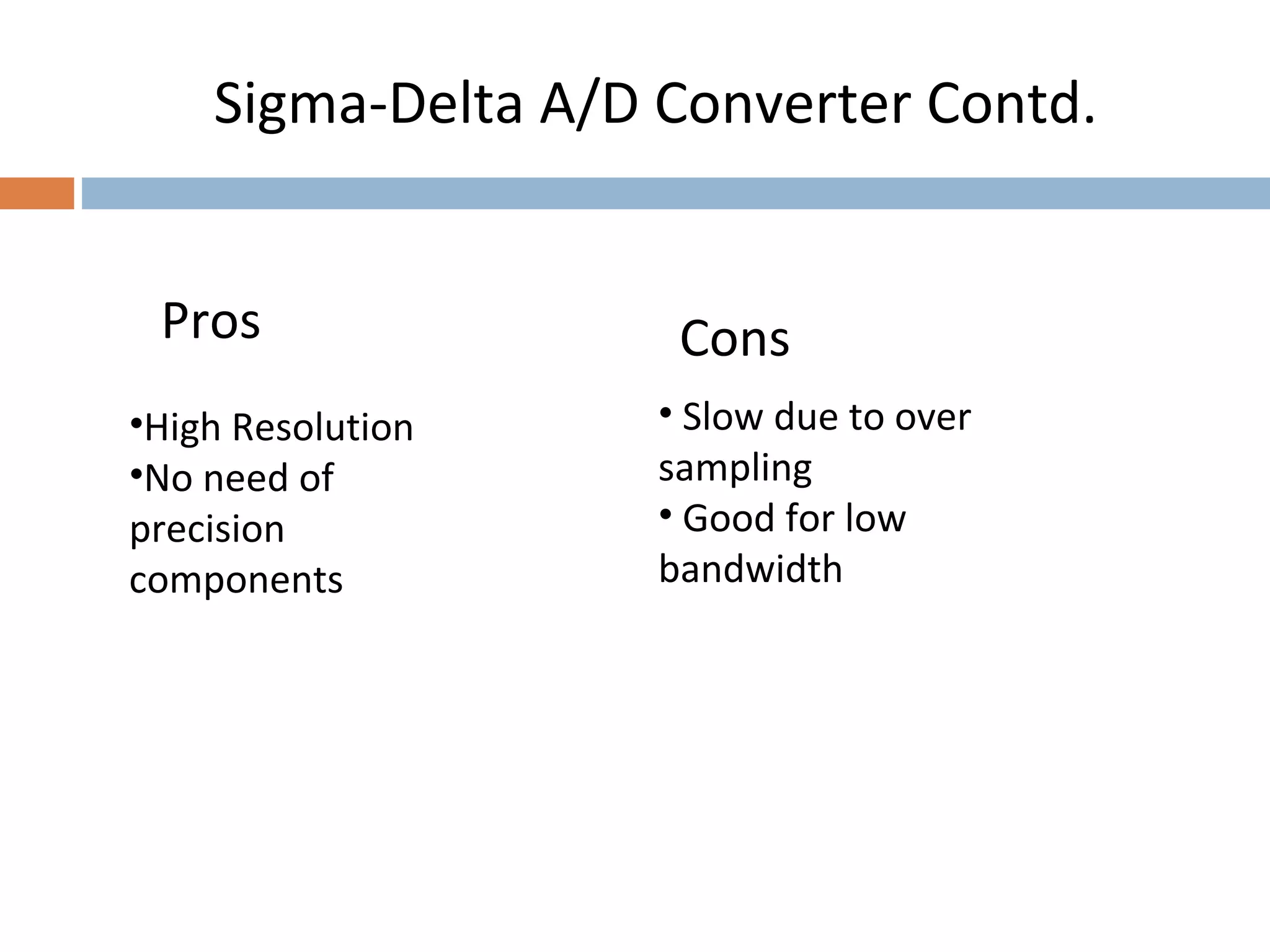
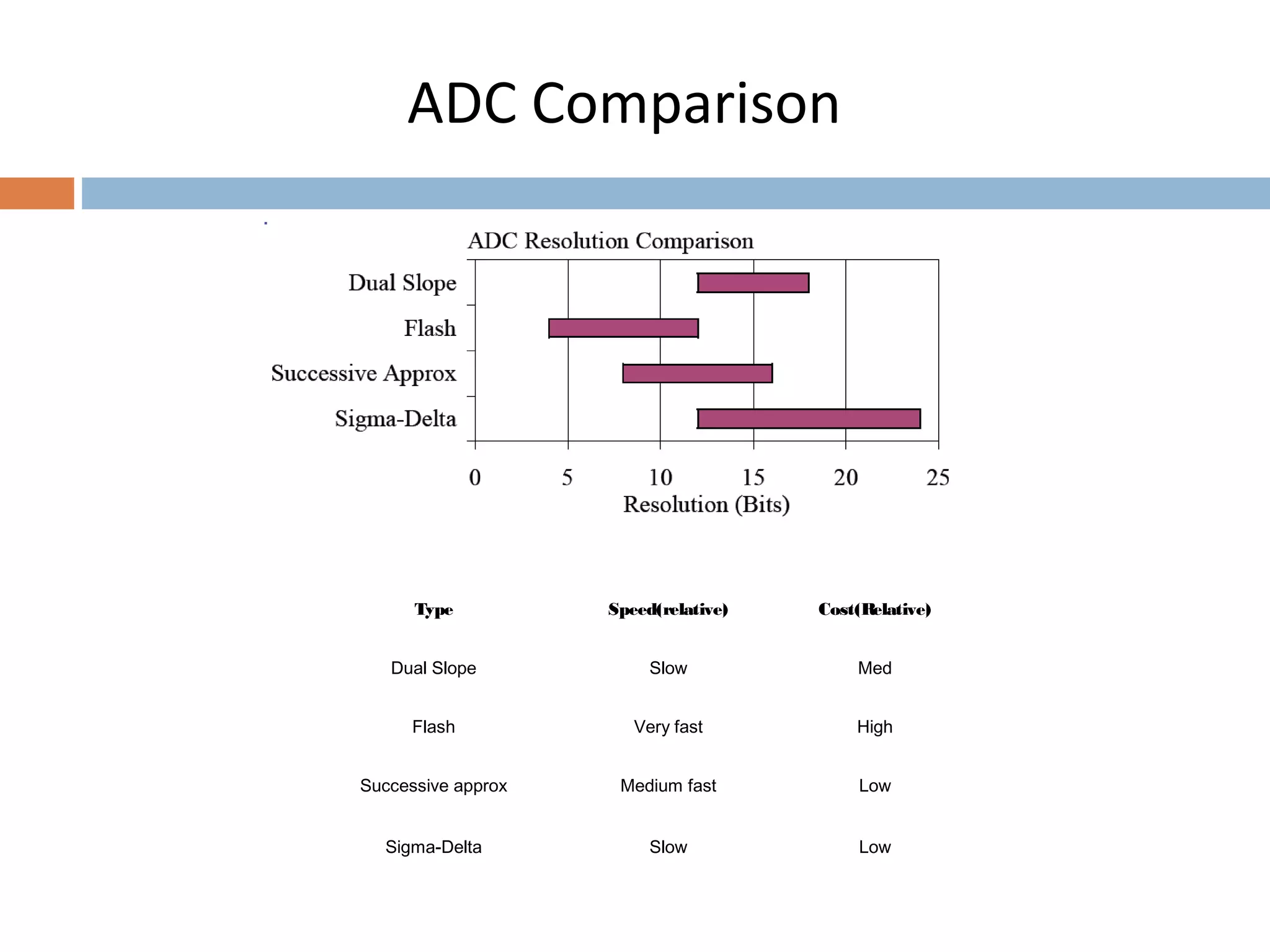
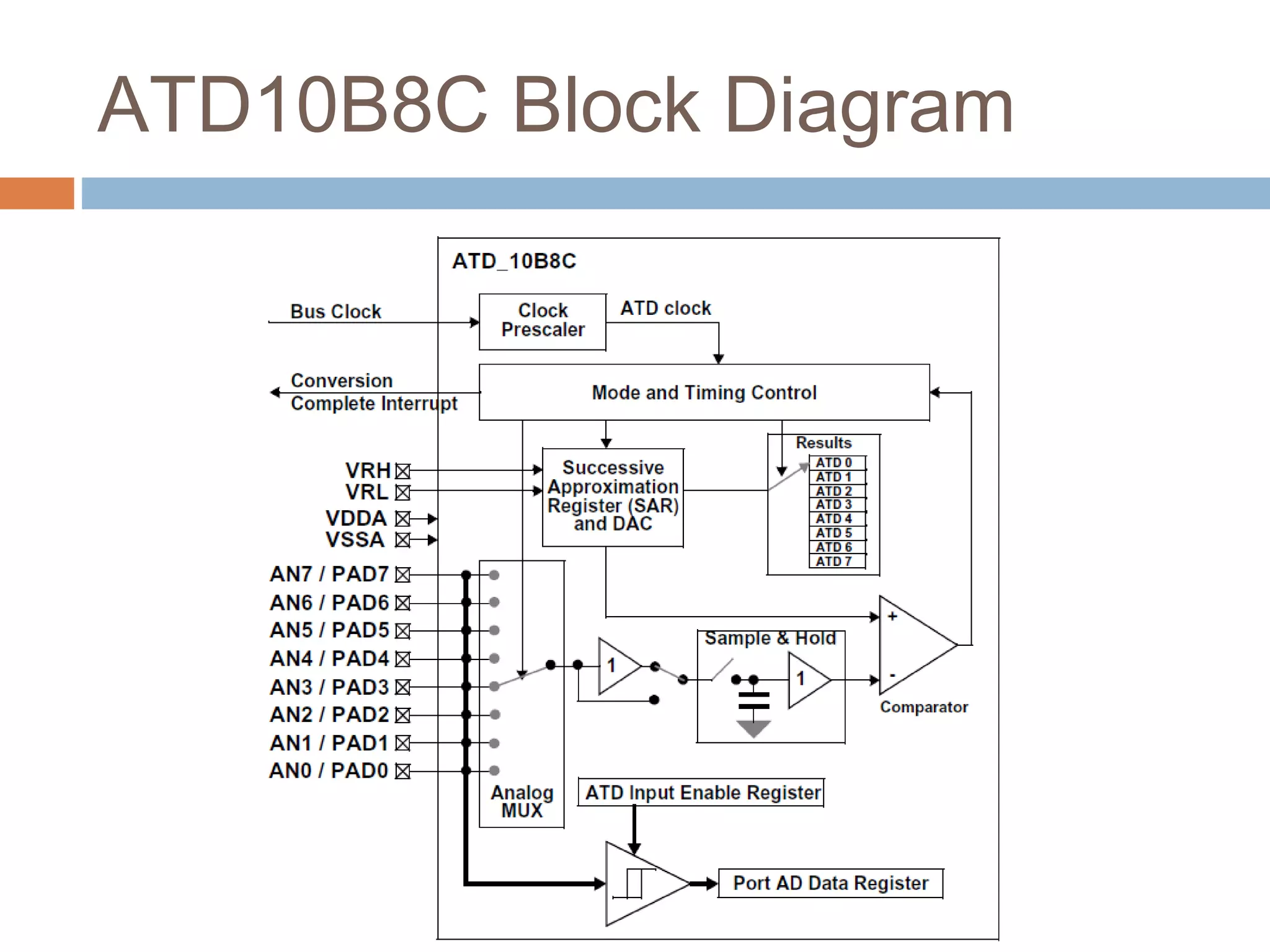
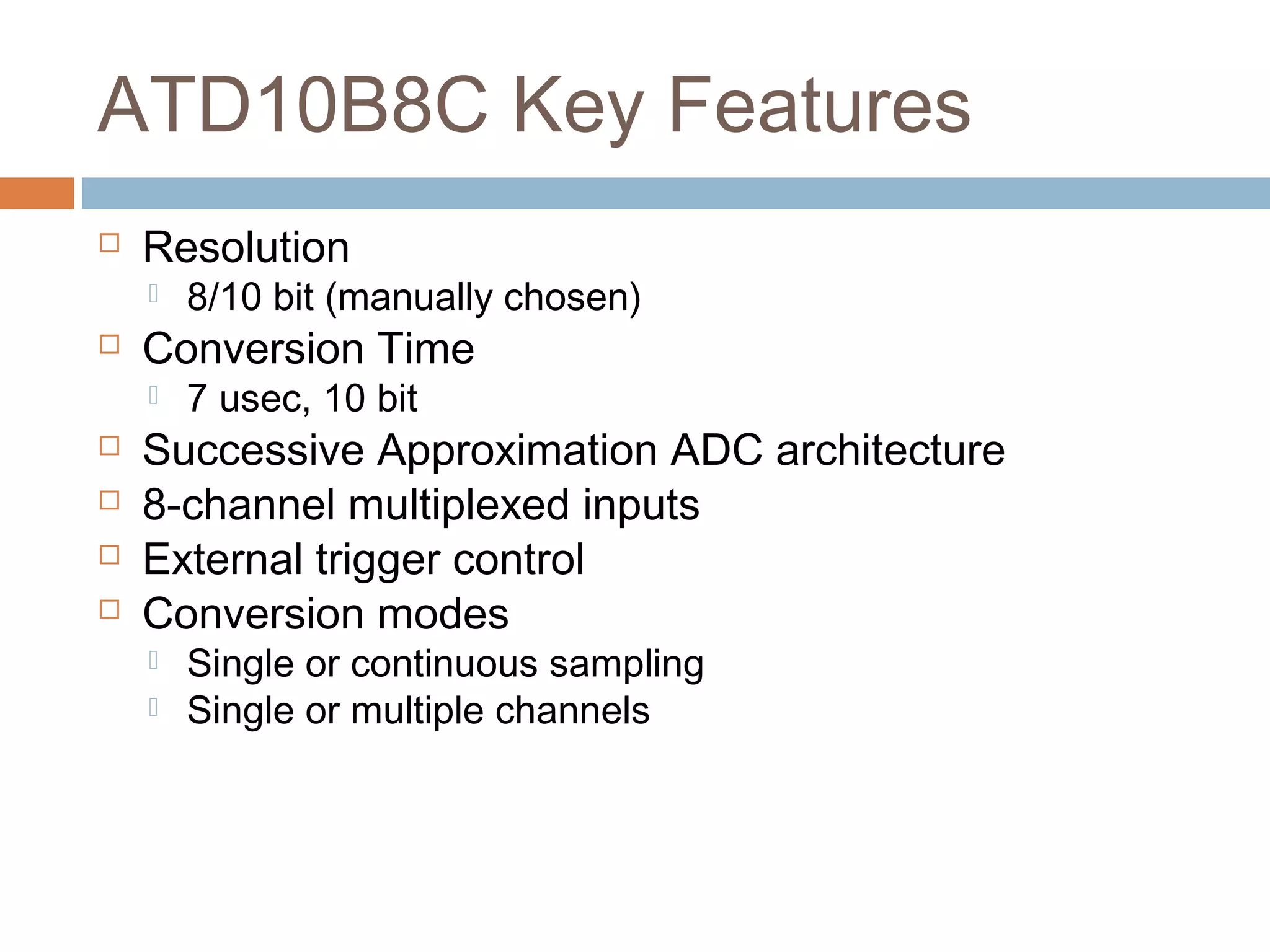
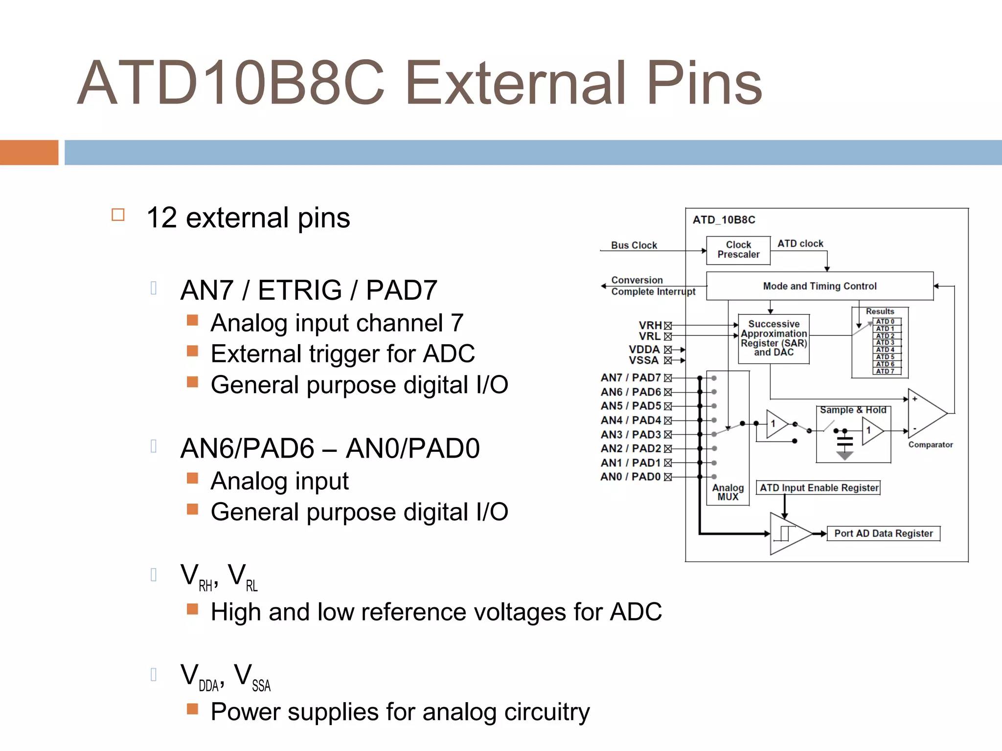
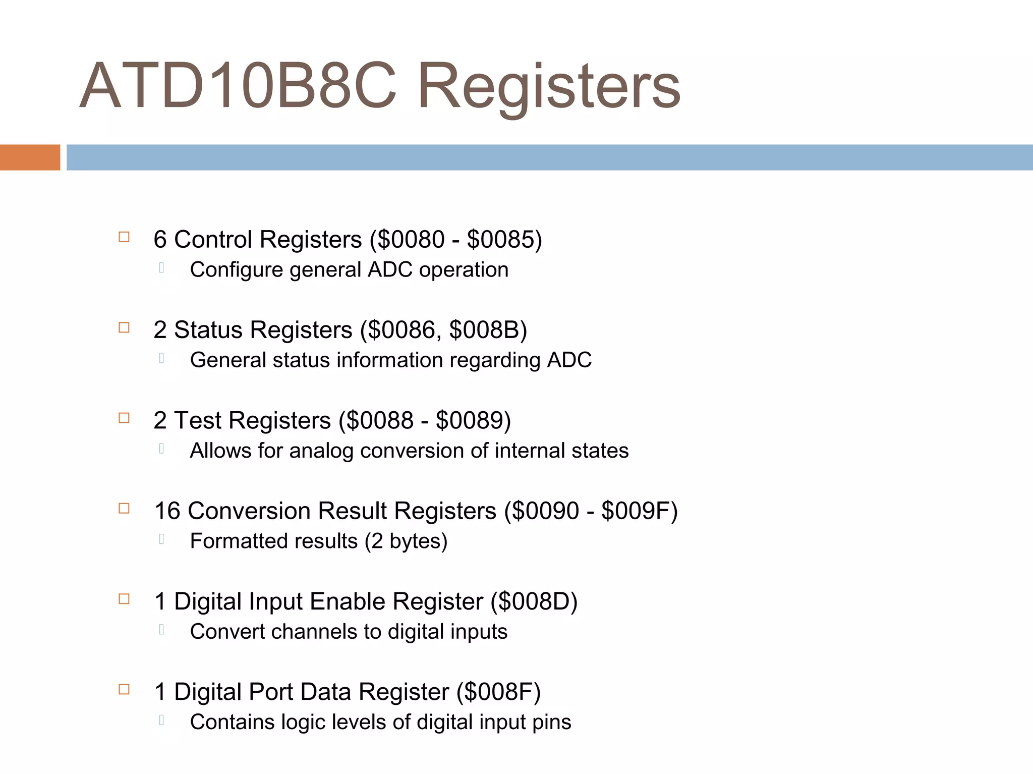
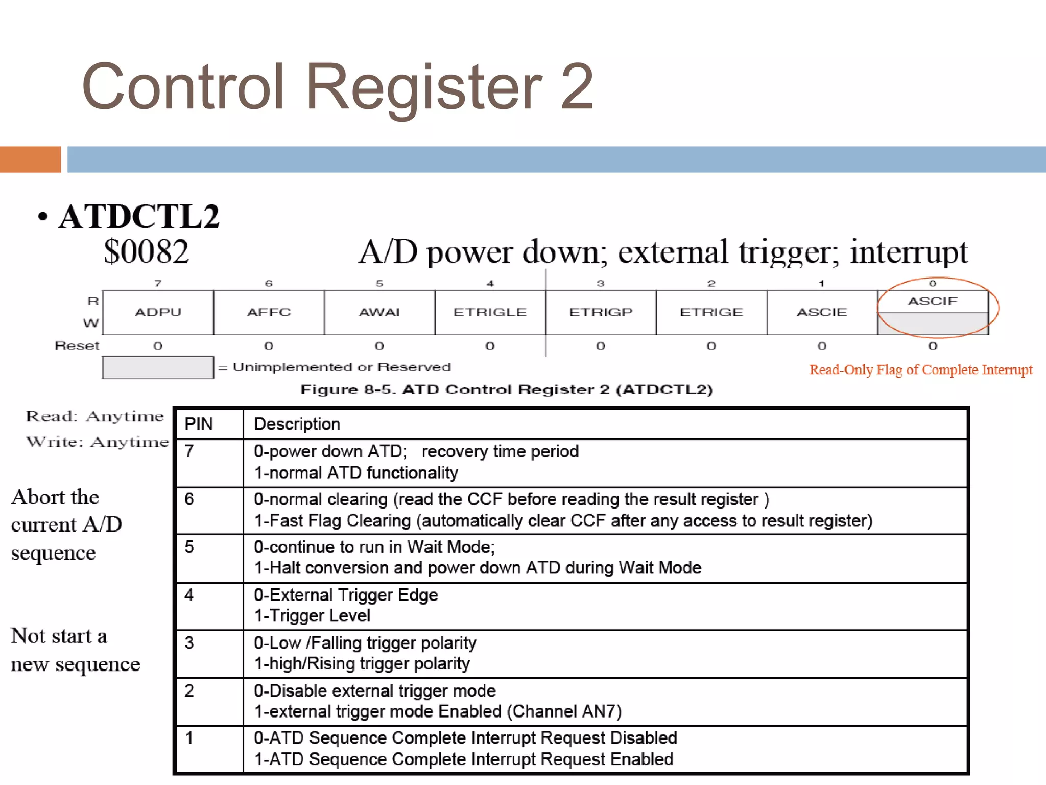
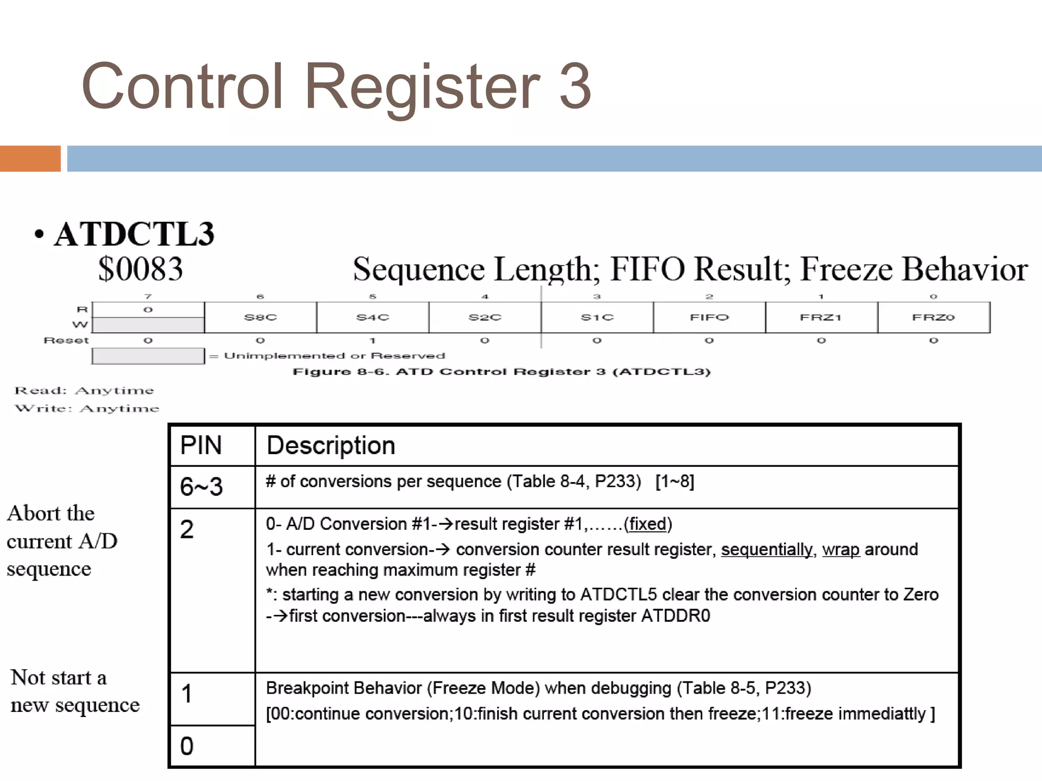
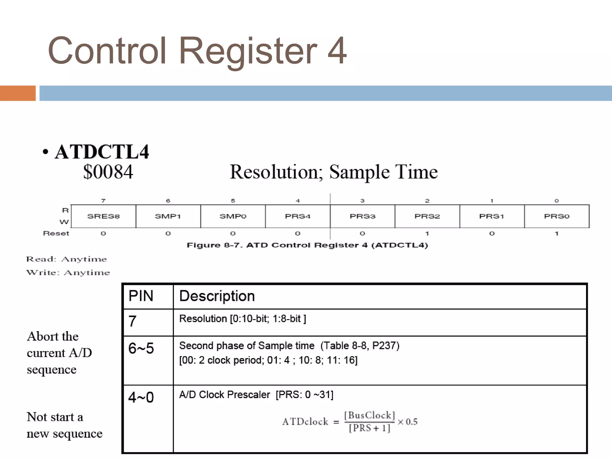
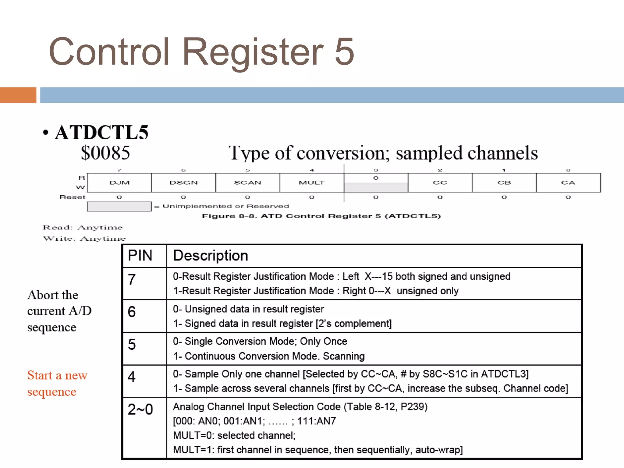
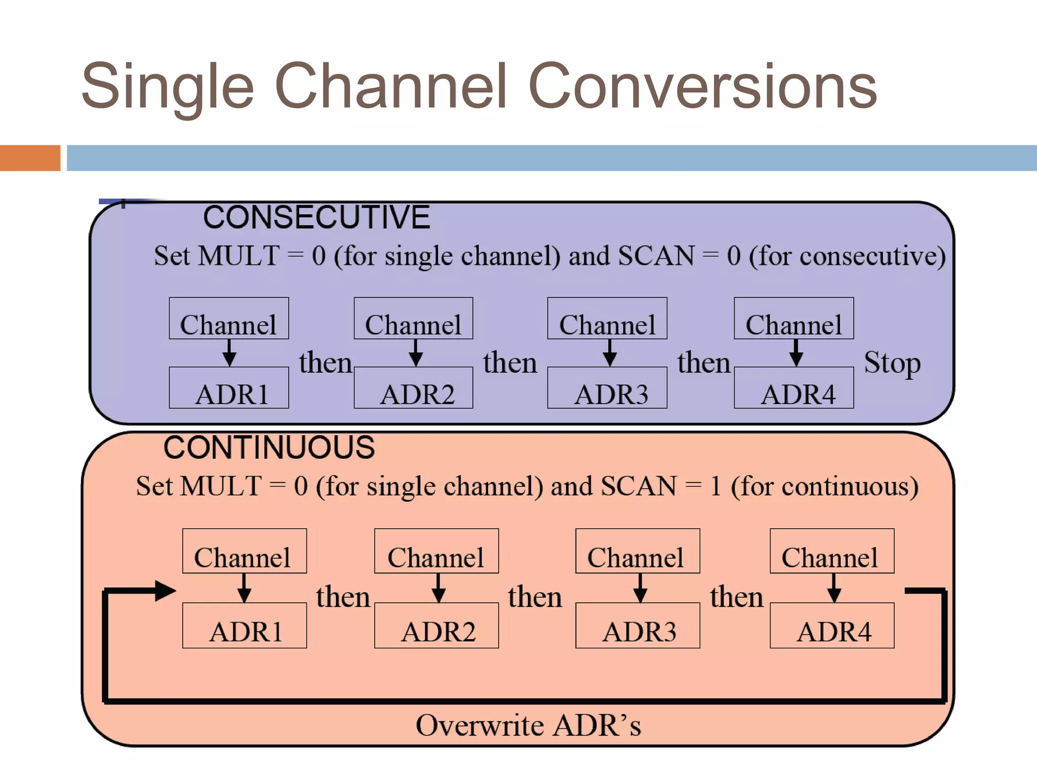
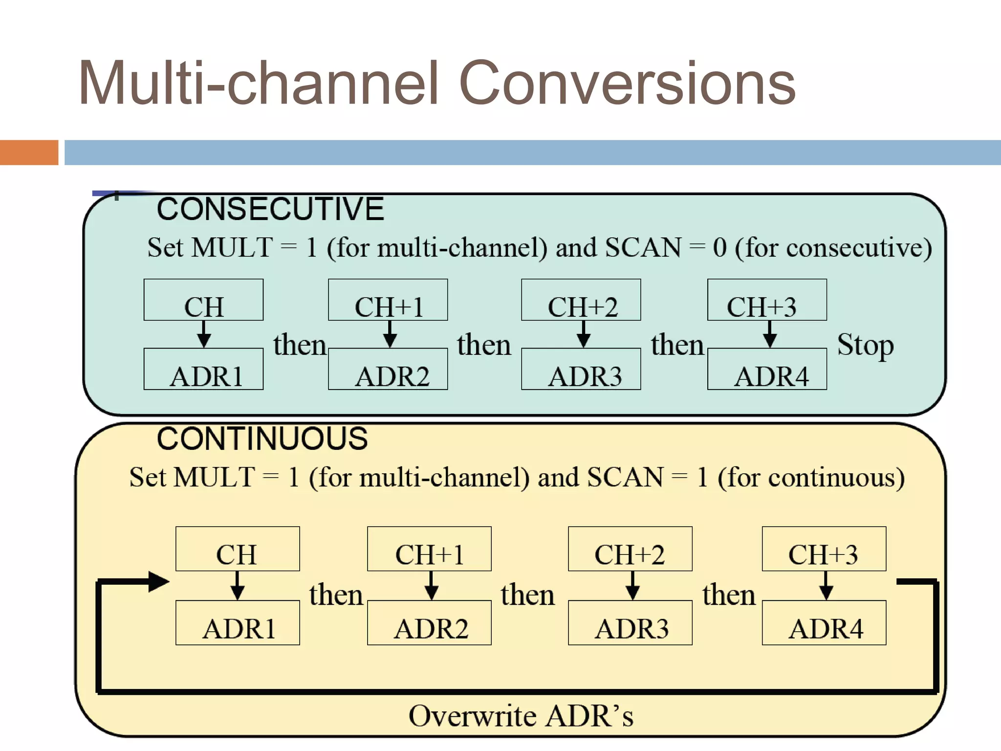
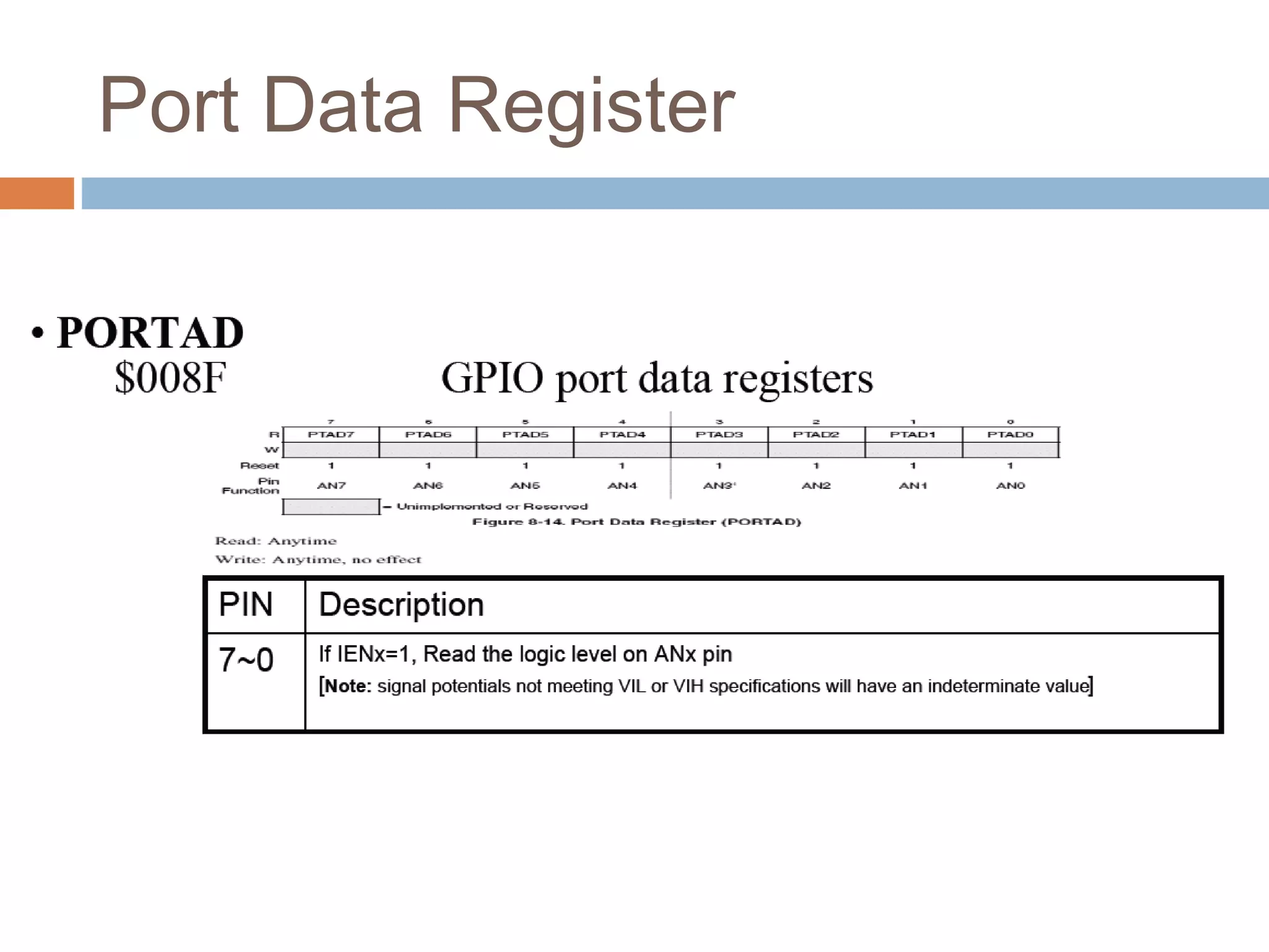
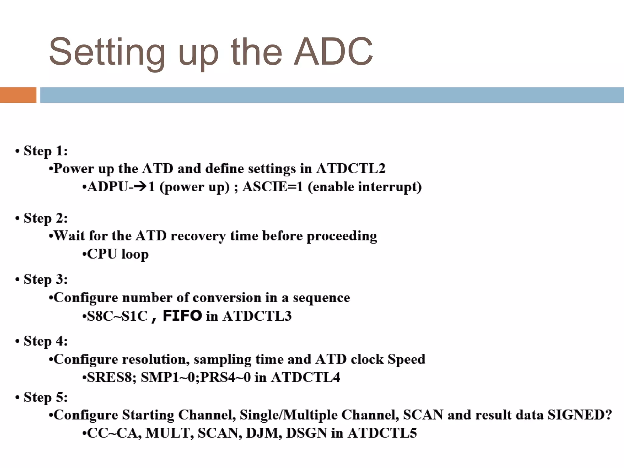
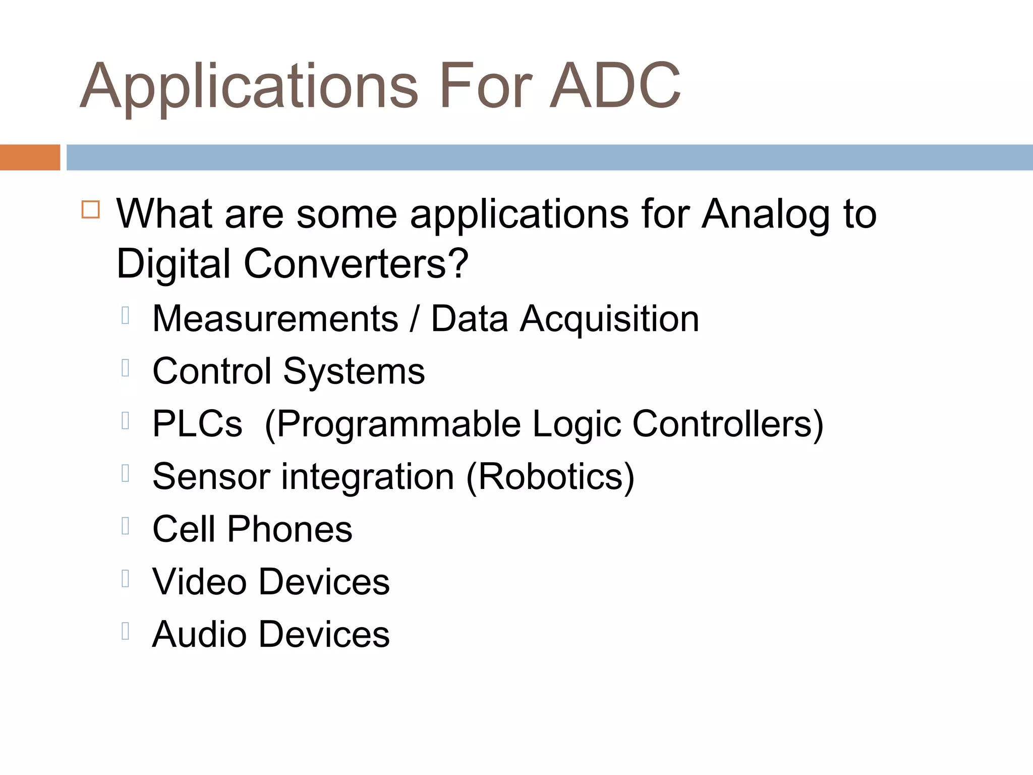
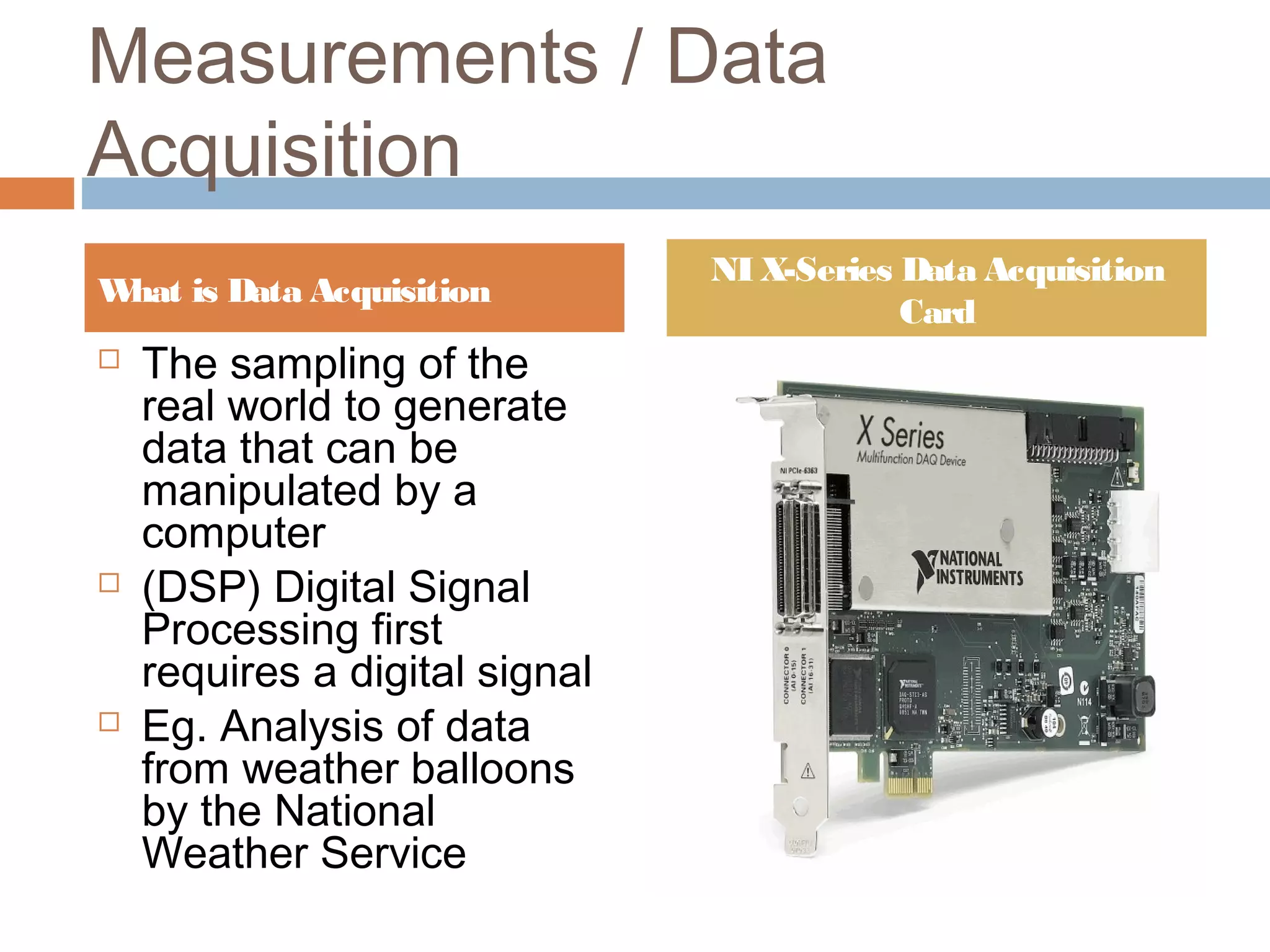
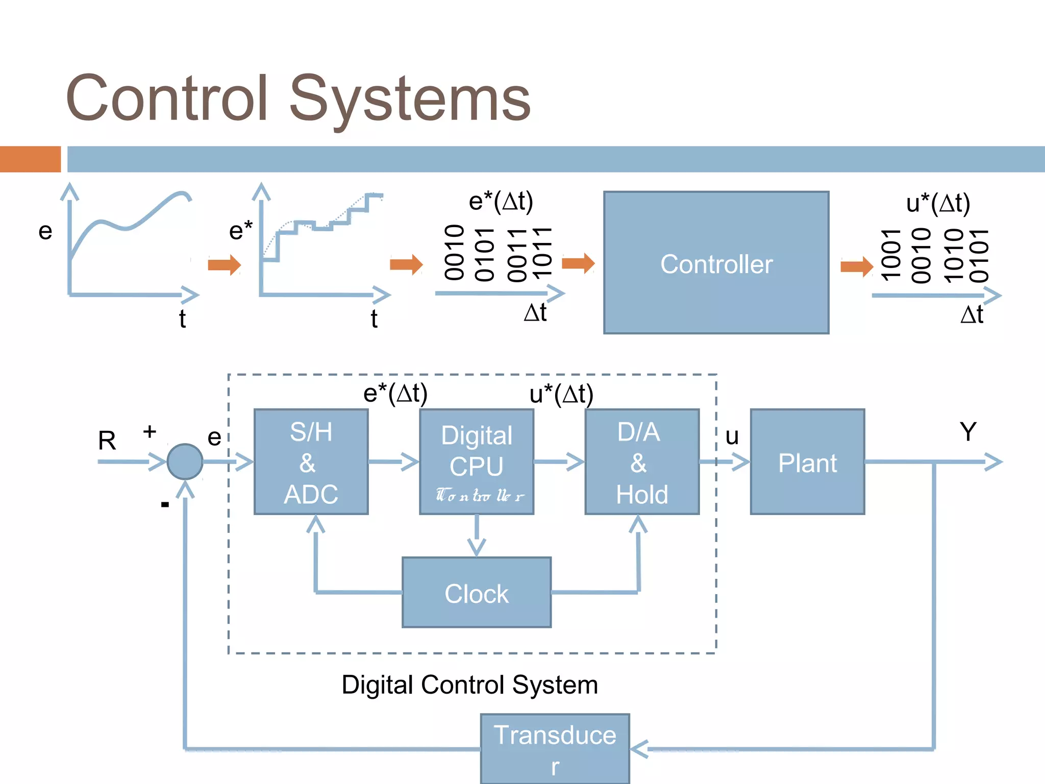
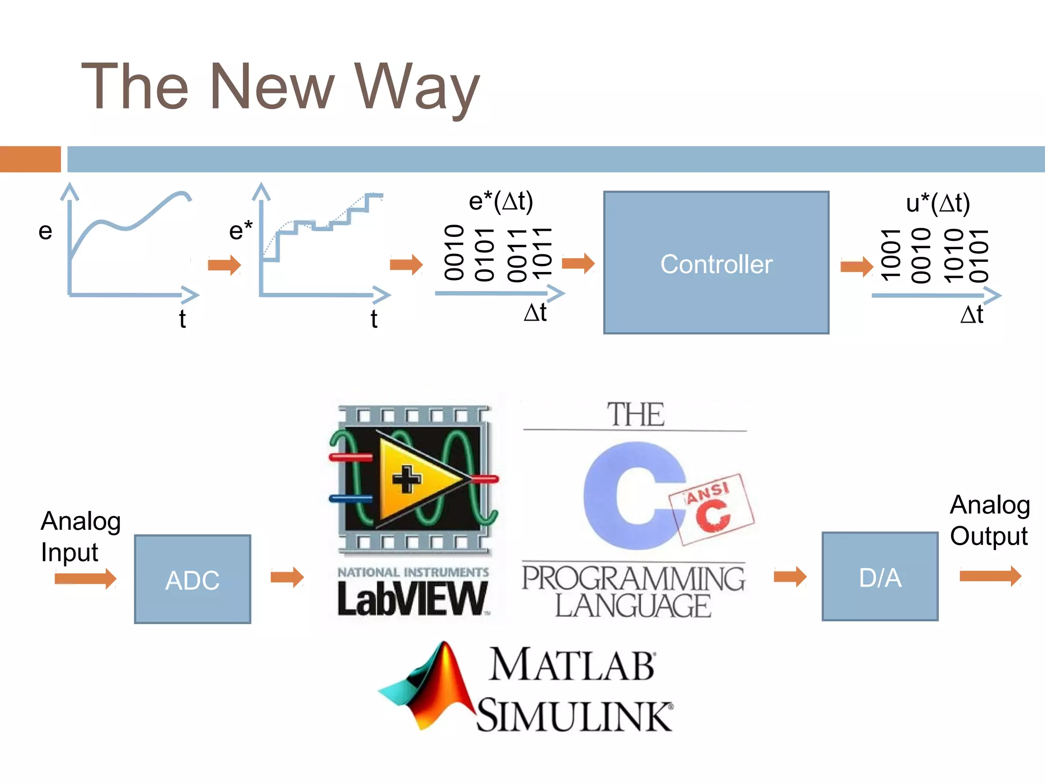
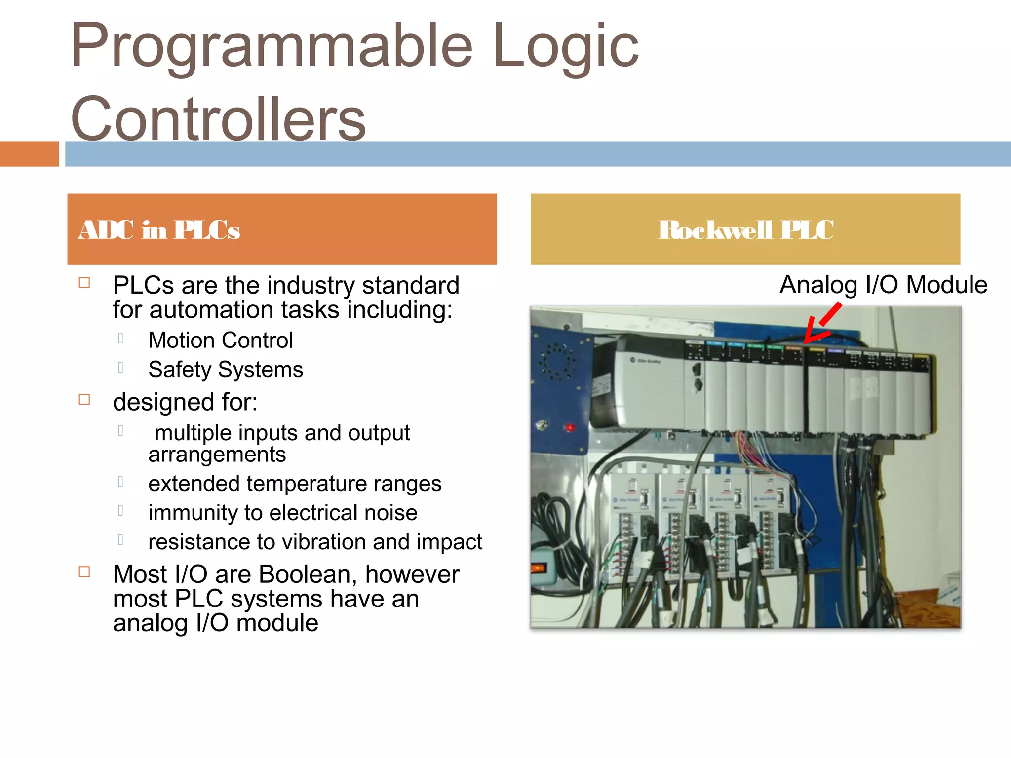


1) The document discusses analog-to-digital converters (ADCs), including their basic function of converting continuous analog signals to discrete digital numbers. 2) It describes several types of ADCs - flash, successive approximation, dual slope, and delta-sigma - along with their relative speeds and costs. 3) The document then focuses on the ATD10B8C ADC present on the MC9S12C32 microcontroller, outlining its key features, registers, and how to set it up and use it to take single-channel or multi-channel conversions.