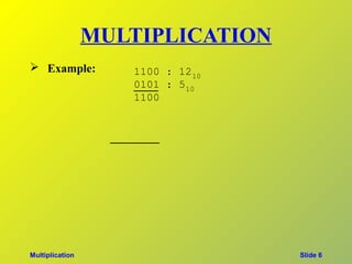
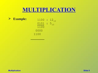
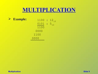
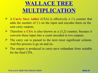
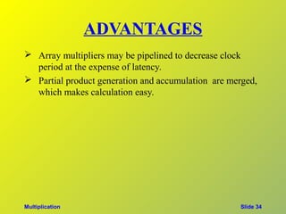
THIS PPT IS PRESENTED TO PROF. RAVITESH MISHRA FROM EC FINAL YEAR STUDENTS MADE FROM RAZAVI,DESIGN OF ANALOG CMOS INTEGRATED CIRCUITS ON DATAPATH SUBSYSTEM-MULTIPLICATION
The document describes the principles and implementation of an array multiplier. It discusses how array multipliers generate partial products simultaneously using parallel logic, making them faster than serial multipliers. A 4x4 bit array multiplier is implemented in Verilog using AND gates and adders, and its functionality is verified through simulation. While array multipliers require more gates and area than serial multipliers, their performance can be increased using pipelining. The document concludes that array multiplication is well-suited for applications requiring high speed.
The document discusses various techniques for accelerating the multiplication process, including shift-and-add, Booth's recoding, and higher radix multipliers. Booth's recoding maps digit sets to [-1,1] to skip additions when partial products are zero. Modified Booth's recoding improves on this by considering three adjacent bits to encode multipliers into [-2,2], allowing the use of radix-4 grouping to reduce the number of partial product additions. Modern multipliers apply Modified Booth's Recoding to take advantage of its higher radix structure.
This document discusses various designs for digital multipliers. It begins by reviewing the basic building blocks used in digital circuits and how binary multiplication works by adding partial products. It then describes approaches for implementing multiplication, including right shift and add serial multipliers and faster parallel array and tree multipliers. Booth encoding is introduced as a technique to reduce the number of stages in a multiplier. Implementation details are provided for array and Wallace tree multipliers, including the use of compression cells like the (4,2) counter. Optimization goals for multipliers differ from adders in emphasizing reducing the critical path.
A state machine is a system that can be described by a set of states that the system transitions through. It has a set of inputs, outputs, and memory. There are two main types - Mealy machines where the output is a function of the state and inputs, and Moore machines where the output is only a function of the state. To design a state machine, you first understand the problem, draw a state diagram, reduce states if possible, assign states, and design the circuit from the state table. An example is a serial adder where each bit is added sequentially using states to track the carry.
THIS PPT IS SO USEFUL FOR THE CONTROL SYSTEM STUDENTS MOSTLY. THIS PPT MAINLY DISCUSSED ABOUT THE IMPULSE RESPONSE OF SECOND ORDER SYSTEM
AND THE CHARACTERISTICS OF THE SYSTEM AND STABILITY FACTOR OF THE SYSTEM AN THIS PPT CONTAINS A MATLAB CODING AND SIMULATION AND THE RESULTS ARE ALSO PLOTED IN THE PPT . SO IT IS SO USEFUL TO THE STUDENTS
This document discusses digital adders and subtracters. It begins by explaining half adders and full adders, which are used to add binary numbers. It then discusses how to design multi-bit adders using full adders as building blocks. Different approaches for subtraction using full adders and full subtracters are also covered. The document provides circuit diagrams and truth tables to illustrate the designs of basic digital addition and subtraction components.
This document describes the design of a Wallace tree multiplier using Verilog. It discusses different types of multipliers such as array, serial/parallel, and Booth multipliers. It provides details on the Wallace tree multiplier design including its block diagram, partitioning of partial products, number of levels, submodules like AND gates and full adders, and comparison of its power consumption and results. The dumping process in an FPGA kit is also covered along with the advantage of small delay and disadvantage of complex layout for the Wallace tree multiplier.
The document summarizes different types of shifters used in microprocessor design including logical, arithmetic, barrel, and funnel shifters. It describes the function of each shifter type and provides examples. It then focuses on funnel shifters, explaining they can perform all shift operations, and describes two types of funnel shifter designs - array and multilevel funnel shifters. The array design uses an array of multiplexers while the multilevel design uses multiple levels of smaller multiplexers.
The document discusses different number systems used in computers such as binary, decimal, hexadecimal, and octal. It explains how computers use binary digits for operations and how different number systems are converted between each other. For example, binary numbers are converted to decimal by multiplying each bit by its place value and summing the results. Negative numbers are represented using ones' complement and twos' complement in binary. Basic logic gates and flip-flops used in digital circuits are also introduced.
Reduction of multiple subsystem [compatibility mode]azroyyazid
This document discusses techniques for reducing multiple subsystems to a single transfer function. It covers block diagram algebra and Manson's rule. Block diagram algebra can be used to reduce block diagrams representing cascaded, parallel, and feedback subsystems into equivalent single transfer functions. The key techniques are collapsing summing junctions and forming equivalent cascaded, parallel, and feedback systems. Signal-flow graphs also represent subsystems and can be reduced using Manson's rule by writing equations for each signal as the sum of incoming signals times their transfer functions. Examples demonstrate reducing various block diagrams and signal-flow graphs to equivalent single transfer functions.
This document provides an overview of signal flow graphs including:
- Definitions and terminology of signal flow graphs
- Examples of constructing signal flow graphs from equations and block diagrams
- Mason's gain formula for calculating the transfer function of a system from its signal flow graph representation in 3 sentences or less
- Examples are provided to demonstrate applying Mason's gain formula to calculate transfer functions from given signal flow graphs.
This document discusses various VLSI testing techniques. It begins by explaining the need for testing circuits when they are first developed and manufactured to check that they meet specifications. The main testing approach is to apply test inputs and compare the outputs to expected patterns. It then describes different testing techniques for combinational and sequential circuits, including fault modeling, path sensitizing, scan path testing, built-in self-test (BIST), boundary scan testing, and signature analysis. Specific circuit examples are provided to illustrate scan path testing, BIST using linear feedback shift registers (LFSRs) and compressor circuits, and boundary scan testing.
This document discusses and compares combinational and sequential circuits. It provides examples of common combinational circuits like half adders, full adders, decoders, and multiplexers. It also discusses sequential circuits elements like flip flops and shift registers. The document then focuses on adders in more detail, explaining half adders, full adders, and ripple carry adders through diagrams and examples.
1. The 8254 contains three independent 16-bit counters/timers that can be programmed to operate in different modes.
2. Each counter can be programmed to count from 1 to 65535 and has a programmable control word to select the operating mode.
3. The 8254 supports various timer modes like one-shot, continuous square wave, event counter, and software/hardware triggered one-shot for applications like timing, delay generation, and pulse width modulation.
DESIGN AND SIMULATION OF DIFFERENT 8-BIT MULTIPLIERS USING VERILOG CODE BY SA...Saikiran Panjala
This document describes the design and simulation of different 8-bit multipliers using Verilog code. It summarizes four multipliers: array, Wallace tree, Baugh-Wooley, and Vedic. It finds that the Baugh-Wooley multiplier has advantages in speed, delay, area, complexity, and power consumption compared to the other multipliers. The document also discusses half adders, full adders, ripple carry adders, carry save adders, and multiplication algorithms. It aims to compare the multipliers based on area, speed, and delay.
This document describes the design and operation of half adders, full adders, half subtractors, and full subtractors. It defines each component, provides their truth tables, and shows how to design the logic circuits using K-maps. Half adders and subtractors perform addition and subtraction of two single bits, while full adders and subtractors handle three input bits, accounting for values carried in and out. The document also distinguishes between the components and their uses in digital logic systems.
The document describes the Modified Booth's Algorithm for binary multiplication of negative numbers. It uses bit pair recoding of the multiplier and defines a recoding table. As an example, it shows the step-by-step binary multiplication of -13 x -7 using bit pair recoding of the multiplier, multiplication according to the recoding table, and addition of partial products to get the final result of 91.
This document discusses multiplexers and de-multiplexers. It defines a multiplexer as a circuit that accepts multiple input signals but provides a single output signal, selecting one input using control signals. A de-multiplexer is the opposite, accepting one input and providing multiple outputs. Examples of 4-to-1 multiplexers and 1-to-4 de-multiplexers are described. Applications include communication systems, computer memory, and transmitting satellite data. Multiplexers and de-multiplexers are commonly used together and are important combinational logic circuits.
The document discusses different methods for multiplication of binary numbers, including combinational and sequential multipliers. A sequential multiplier uses one parallel adder, registers capable of shifting, and control logic. It multiplies digits through addition and shifting the registers. For signed multiplication, the multiplier and multiplicand may need to be complemented depending on their signs. Booth's algorithm can multiply signed numbers by adding or subtracting the multiplicand instead of just adding, reducing the number of operations.
Poles and Zeros of a transfer function are the frequencies for which the value of the denominator and numerator of transfer function becomes zero respectively
1) The document discusses parallel adders and subtractors for n-bit binary numbers. It specifically examines a 4-bit parallel adder that uses full adders connected in cascade, with the carry output of one full adder connected to the next's carry input.
2) A 4-bit parallel subtractor is also examined, which takes the 2's complement of the number to be subtracted and adds it to the other number using a 4-bit parallel adder.
3) Carry propagation time is discussed, which is the time it takes the carry to ripple through all the full adders in the parallel adder from the least to most significant bit.
The document summarizes the design and analysis of the uA741 operational amplifier, which was one of the most popular op-amps ever made. It describes the op-amp's stages including input, gain, and output stages. It also analyzes the op-amp's DC bias point, small signal behavior through frequency and transient analysis, and how it performs under variations through Monte Carlo analysis. The document shows that the uA741 design is robust to changes in components and operates as intended across a wide range of conditions.
Chapter 01 Basic Principles of Digital SystemsSSE_AndyLi
This document provides an overview of digital systems fundamentals, including:
- Analog signals have continuous values while digital signals can only have discrete values (0 or 1).
- Digital electronics uses binary logic levels to represent information, with a high voltage representing 1 and a low voltage representing 0.
- The binary number system uses positional notation to represent numbers using only the digits 0 and 1.
- Digital circuits operate on binary inputs and outputs, with truth tables listing all possible input-output combinations for a logic gate or circuit.
This document provides an analysis of different logic full adders. It begins with an introduction on the need for adders and their basic parameters such as power consumption, speed, area, and delay. It then discusses various full adder circuit designs including C-CMOS logic, CPL, DPL, transmission gate, transmission function, 14T, and GDI XOR/XNOR full adders. For each design, the document outlines the number of transistors used, speed, power dissipation, and other characteristics. It concludes with a comparison table of the delay, average power, power-delay product, and number of transistors for each full adder design.
VLSI subsystem design processes and illustrationVishal kakade
This document discusses the design processes for digital subsystem design. It begins by outlining the objectives of design consideration, problem and solution, basic digital processor structure, and datapath. It then discusses general considerations for subsystem design such as lower unit cost and higher reliability. It presents some common problems in design like how to design complex systems efficiently. It proposes solutions like top-down design and partitioning the system. The document then illustrates the design processes through examples like designing a 4-bit shifter and ALU subsystem. It provides block diagrams, logic diagrams and layouts at different stages of the design process.
The document discusses the benefits of digital integrated circuits including lower unit cost, higher reliability, lower power dissipation, reduced weight and volume, better performance, enhanced repeatability, and possibly reduced design and development periods. It also lists common representations used in digital design such as conventional circuit symbols, logic symbols, stick diagrams, mask layouts, and architectural block diagrams and floor plans. Finally, it provides three examples of sequences for operations in a basic digital processor involving transferring operands from registers to an ALU, performing operations in the ALU, and storing results either back in registers or after passing through a shifter.
Seminar on Digital Multiplier(Booth Multiplier) Using VHDLNaseer LoneRider
This is my Mini project. It is very clear and has lots of animation in it. If you like to know about booth algorithm and VHDL this the perfect presentation. Download it and see as SLIDE SHOW. You will enjoy more of my work, Give blessings.
This document discusses Wallace tree multiplication. It begins by explaining the basic concept of a Wallace tree multiplier using 1-bit full adders to compress the number of bits at each stage. It then provides examples of 6x6 multipliers using Wallace trees. It notes that a 32-bit multiplier using this method would have 9 adder delays. Finally, it asks questions about extending this to a 64-bit multiplier and whether other compression schemes could reduce the delay further.
Design and Simulation of Radix-8 Booth Encoder Multiplier for Signed and Unsi...ijsrd.com
This paper presents the design and simulation of signed-unsigned Radix-8 Booth Encoding multiplier. The Radix-8 Booth Encoder circuit generates n/3 the partial products in parallel. By extending sign bit of the operands and generating an additional partial product the signed of unsigned Radix-8 BE multiplier is obtained. The Carry Save Adder (CSA) tree and the final Carry Look ahead (CLA) adder used to speed up the multiplier operation. Since signed and unsigned multiplication operation is performed by the same multiplier unit the required hardware and the chip area reduces and this in turn reduces power dissipation and cost of a system. The simulation is done through Verilog on xiling13.3 platform which provide diversity in calculating the various parameters.
VLSI Implementation of High Speed & Low Power Multiplier in FPGAIOSR Journals
Abstract : We known that different multipliers consume most of the power in DSP computations, FIR filters.
Hence, it is very important factor for modern DSP systems to built low-power multipliers to minimize the power
dissipation. In this paper, we presents high speed & low power Row Column bypass multiplier design
methodology that inserts more number of zeros in the multiplicand thereby bypass the number of zero in row &
Column as well as reduce power consumption. The bypassing of zero activity of the component used in the
process of multiplication, depends on the input bit data. This means if the input bit data is zero, corresponding
row and column of adders need not be addition & transfer bit in next row and column adder circuit. If
multiplicand having more zeros, higher power reduction can be achieved. At last stage of Row & column bypass
multiplier having ripple carry adder which are increase time to generate carry bit to transfer next adder
circuit. To reduce this problem by using Carry bypass adder in place of ripple carry adder, then new
modification of Row &column multiplier having high speed in comparison to simple row & column bypass
multiplier, , the experimental results show that our proposed multiplier reduces power dissipation & High
speed overhead on the average for 4x4, 8x8 and 16x16 multiplier.
Keywords: Low Power, Row & Column bypass Multiplier, Carry bypassing techniques, FPGA, Xilinx
This document presents Booth's radix-4 algorithm for performing binary multiplication using an ALU. It explains that Booth's algorithm reduces the number of partial products generated during multiplication by grouping consecutive zeros and ones. It then describes the radix-2 Booth's algorithm and provides an example. The drawbacks of radix-2 are discussed, such as its inefficiency with isolated ones. Next, the radix-4 coding technique is presented and an example is shown. Finally, VHDL simulation code is presented to simulate multiplication using radix-4 algorithm.
This document discusses the design and implementation of a carry save multiplier integrated circuit project supervised by Dr. Sayed Eid. It describes using a carry save multiplier algorithm that divides the multiplier into blocks, including bit multiplication, half adders, and full adders. It also discusses implementing the algorithm in Matlab, Simulink, and Verilog, and comparing the area and delay of different multiplier designs synthesized on an FPGA.
Performance Analysis of Encoder in Different Logic Techniques for High-Speed ...Achintya Kumar
In designing a system, we can replace cell components by appropriate technique based cell so that the noise margin of overall circuit is improved. In future we can also implement some techniques for sequential circuits.
This document discusses the performance analysis of different CMOS full adder circuits and the VLSI design of a multiplier using Mentor Graphics. It analyzes the performance of various full adder circuits in terms of delay, power dissipation, and power-delay product. The high-performance 8T full adder is identified and used in the design of 4x4 multipliers like array, Braun, Baugh-Wooley, and Wallace tree multipliers. The multipliers are then analyzed and compared based on their complexity and performance.
A High Speed Wallace Tree Multiplier Using Modified Booth Algorithm for Fast ...Kumar Goud
Abstract— Designing multipliers that are of high-speed, low power, and regular in layout are of substantial research interest. Speed of the multiplier can be increased by reducing the generated partial products. Many attempts have been made to reduce the number of partial products generated in a multiplication process; one of them is Wallace tree multiplier. Wallace Tree CSA structures have been used to sum the partial products in reduced time. In this paper Wallace tree construction is investigated and evaluated. Speed of traditional Wallace tree multiplier can be improved by using compressor techniques. In this paper Wallace tree is constructed by traditional method and with the help of compressor techniques such as 4:2 compressor, 5:2 compressor, 6:2 compressor, 7:2 compressor. Therefore, minimizing the number of half adders used in a multiplier reduction will reduce the complexity.
Index Terms—Component, formatting, style, styling, insert. (key words)
A datapath is a collection of functional units like ALUs and registers that perform data processing along with a control unit to form the CPU. There are three general steps to datapath design: 1) determine instruction classes, 2) design components for each class, and 3) combine the components. Common datapaths include load/store which uses memory addressing and branch/jump which uses instruction addressing. The ALU performs operations like addition and subtraction. The main control unit identifies instruction fields and controls the datapath. Multiplication can be done with combinational or sequential circuits while division similarly uses subtraction and shifting. Floating point uses separate exponent and mantissa fields.
The document discusses integer multiplication and division techniques in binary. It describes how unsigned and signed multiplication can be performed sequentially by shifting and adding the multiplicand. For division, the dividend is shifted left while subtracting the divisor, with the quotient and remainder stored in registers. Faster multiplication uses multiple adders in parallel, and division similarly shifts and subtracts to iteratively derive the quotient digits. MIPS instructions like mult and div operate on registers to perform 32-bit integer operations.
DESIGN OF SIMULATION DIFFERENT 8-BIT MULTIPLIERS USING VERILOG CODE BY SAIKIR...Saikiran perfect
This project compares 4 different 8-bit multipliers - Wallace tree, array, Baugh-Wooley, and Vedic multipliers - using Verilog code. Simulations show that Wallace tree multipliers consume more power than array multipliers. Array multipliers are preferred for low power applications. The project designs and simulates the multipliers to analyze power consumption and determine the best option for low power, high speed applications like DSP systems.
Information management is concerned with the infrastructure used to collect, manage, store, and deliver information, as well as guiding principles to make information available to the right people at the right time. It encompasses people, processes, technology, and content. The purpose of information management is to design, develop, manage, and use information with insight and innovation to support decision making. It involves gathering information from various sources and organizing it through different stages from tagging to structuring and archiving. Managing information successfully requires competencies across several knowledge and process areas. Common challenges organizations face include disparate systems, lack of integration, outdated legacy systems, and poor information quality.
The document describes two types of high-speed low-power multipliers: the Braun array multiplier and Booth's multiplication algorithm. The Braun multiplier uses an array of AND gates and adders to generate partial products in parallel. Booth's algorithm reduces the number of partial products by recoding the operands. Both multipliers are suitable for high-speed applications but the Braun multiplier has higher complexity and power requirements for large operands sizes.
This document discusses dynamic logic circuits. It notes that dynamic logic circuits offer advantages over static logic circuits by temporarily storing charge in parasitic capacitances rather than relying on steady-state behavior. Dynamic logic circuits require periodic clock signals to control charge refreshing and allow for simple sequential circuits with memory. They can implement logic in smaller areas and thus consume less power than static logic. The document then discusses several examples of dynamic logic circuits like dynamic CMOS TG logic, domino CMOS logic, NORA logic, and their operating principles. It also covers issues like charge leakage and charge sharing that need to be addressed in dynamic logic circuits.
The document discusses various digital circuit techniques for arithmetic operations like addition and multiplication. It covers binary adders, full adders, ripple carry adders, carry lookahead adders, carry save adders, array multipliers, Wallace tree multipliers, and other basic datapath elements. The document also discusses design considerations like transistor count, critical path, performance, power, and layout strategies.
This document discusses carry lookahead adders. It explains that carry lookahead adders improve speed by reducing the time needed to determine carry bits. It describes how carry lookahead adders work by calculating whether each digit position will propagate a carry and combining these values to deduce carries. The document also discusses implementing carry lookahead adders using groups to reduce span and adding additional levels of carry lookahead to handle more bits.
This document discusses various low power multiplier architectures, including Vedic, Booth, and Baugh-Wooley multipliers. It begins with an introduction to low power multipliers and their importance in modern electronics. It then provides overviews of common multiplier types and their working principles, such as shift-and-add, array, and Wallace tree multipliers. The document proceeds to describe signed and unsigned multiplication examples. It focuses on the Vedic, Booth, Baugh-Wooley, Braun, and modified Booth multiplier architectures. Diagrams and equations are provided to illustrate the working of each type.
This document discusses the design and implementation of a modified Booth multiplier on an FPGA. It begins with an introduction to fixed-width multipliers and the truncation error that occurs. It then describes how the partial product matrix of a Booth multiplier can be modified to reduce this error. The rest of the document details the implementation, including the modified Booth encoder and decoder, generation of partial products, shifting of partial products, two's complement arithmetic, addition of partial products, and comparison of the modified Booth multiplier to a standard multiplier in terms of complexity, power consumption, and delay.
The document introduces computer architecture and system software. It discusses the differences between computer organization and computer architecture. It describes the basic components of a computer based on the Von Neumann architecture, which consists of four main sub-systems: memory, ALU, control unit, and I/O. The document also discusses bottlenecks of the Von Neumann architecture and differences between microprocessors and microcontrollers. It covers computer arithmetic concepts like integer representation, floating point representation using IEEE 754 standard, and number bases conversion. Additional topics include binary operations like addition, subtraction using complements, and multiplication algorithms like Booth's multiplication.
Computer organization and architecture lab manual Shankar Gangaju
This document contains information about a computer organization and architecture lab. It includes details about the lab report format, integer representation using fixed point, two's complement, addition and subtraction algorithms and hardware. It also discusses logical operations, and provides MATLAB code examples for 4-bit binary addition, subtraction, multiplication and restoring division algorithms.
Implementation and Simulation of Ieee 754 Single-Precision Floating Point Mul...inventionjournals
International Journal of Engineering and Science Invention (IJESI) is an international journal intended for professionals and researchers in all fields of computer science and electronics. IJESI publishes research articles and reviews within the whole field Engineering Science and Technology, new teaching methods, assessment, validation and the impact of new technologies and it will continue to provide information on the latest trends and developments in this ever-expanding subject. The publications of papers are selected through double peer reviewed to ensure originality, relevance, and readability. The articles published in our journal can be accessed online.
Development of an Algorithm for 16-Bit WTMIOSR Journals
This document describes the development of an algorithm for a 16-bit Wallace tree multiplier (WTM). It begins with an overview of binary multiplication methods and why the Wallace tree structure is advantageous in reducing propagation delay. The document then discusses improvements made to the basic WTM algorithm, including a new method for generating partial products using fewer logic gates. It presents the design, synthesis and testing of WTM circuits of varying sizes on a Spartan-3E FPGA board. Performance metrics like delay, area, power-delay product and area-delay product are measured and compared to other multipliers. The 16-bit WTM is found to have superior performance to the other multipliers in terms of delay, area and speed.
This document describes the development of an algorithm for a 16-bit Wallace tree multiplier (WTM). It begins with background on binary multipliers and discusses methods like ripple carry array and Wallace trees. The Wallace tree approach is analyzed in more detail, outlining its three main steps: partial product generation, reduction stages using adders, and final addition. The document then proposes improvements to the partial product generation step to reduce complexity from O(n2) to O(n). It also presents a scheme for clearly representing signals in the different reduction stages. Finally, the design is synthesized for an FPGA and simulation results are shown comparing the WTM to other multipliers in terms of delay, area, power-delay product,
This document discusses the design of a floating point multiplier. It begins by explaining the representation of floating point numbers with sign, exponent, and significand. It then describes why floating point is used over fixed point for its wider range of values and greater precision over integers. The key steps for multiplying floating point numbers are described as adding the exponents and multiplying the significands, while XORing the signs. Block diagrams and techniques for partial product generation and accumulation are presented, including radix-4 Booth multiplication and use of carry save adders and ripple carry adders. Finally, floating point formats for single, double, and quadruple precision are shown along with using the divide and conquer technique for higher precision multiplication.
This document discusses binary arithmetic operations including addition, subtraction, multiplication, and division that computers perform at a hardware level. It provides examples of how each operation is completed in binary format step-by-step, following specific rules like two's complement for subtraction. Key concepts covered are binary number representation, bit shifting for multiplication and division, and carrying/borrowing for addition and subtraction.
The document provides instructions for an experiment involving writing assembly language programs to perform various arithmetic operations and sort an array using an 8086 microprocessor kit, including adding, subtracting, multiplying, and dividing two numbers and sorting an array in ascending and descending order, with algorithms and sample programs provided.
This document discusses various methods for improving the performance of multiplication operations, including using shifts and adds instead of actual multiplication, and Booth's algorithm. It examines these methods through examples of multiplying pairs of hexadecimal numbers. Booth's algorithm works by repeatedly adding or subtracting the multiplicand based on examining pairs of bits in the multiplier, allowing multiplication to be performed with only shifts. The document also covers non-restoring and non-performing division algorithms.
1) The ALU performs arithmetic operations like addition, subtraction, multiplication and division on fixed point and floating point numbers. Fixed point uses integers while floating point uses a sign, mantissa, and exponent.
2) Binary numbers are added using half adders and full adders which are logic circuits that implement addition using truth tables and K-maps. Subtraction is done using 1's or 2's complement representations.
3) Multiplication is done using sequential or Booth's algorithm approaches while division uses restoring or non-restoring algorithms. Floating point uses similar addition and subtraction steps but first normalizes the exponents.
Addition and subtraction with signed magnitude data (manocs19club
1) There are several algorithms for performing multiplication and division with signed-magnitude numbers, including array multiplication, Booth's multiplication, restoring division, and non-restoring division.
2) Hardware implementations of these algorithms often involve adders, shifters, and correction logic to handle issues like overflow and producing results in the proper number format.
3) Division algorithms in particular require handling issues like division by zero and divide overflow through detection logic and interrupt-driven error handling.
Arithmetic Unit Addition Subtraction Multiplication and DivisionRNShukla7
1) There are several algorithms for performing multiplication and division with signed-magnitude numbers, including array multiplication and Booth's multiplication.
2) Hardware designs for signed-magnitude addition/subtraction, BCD addition, and restoring division are also covered. These designs make use of components like full adders, correction logic, and shift registers.
3) Special cases like overflow and division by zero must be handled to ensure correct operation of multiplication and division circuits. Interrupts can help handle errors caused by conditions like overflow.
The document describes the linear programming problem and the simplex method for solving it. It provides an example problem of determining the optimal product mix for two products to maximize total income. The summary is:
(1) The example problem involves determining the optimal levels of two products given constraints on raw materials, storage space, and production time to maximize total income.
(2) The simplex method is applied by setting up the linear programming model, identifying entering and leaving variables, and performing row operations to iteratively find a better solution until reaching an optimal solution.
(3) For the example, the optimal solution found through three iterations of the simplex method is to produce 270 units of the first product and 75
This document provides an overview of digital systems and information representation. It discusses key topics such as number systems, arithmetic operations, and coding. Digital systems take discrete inputs and outputs and can have state. There are different types including combinational and sequential systems. Information is represented using physical quantities mapped to discrete values, often binary digits. Common number systems like binary, octal, hexadecimal and their arithmetic are covered. Conversion between number systems and different number bases is also explained.
Error Reduction of Modified Booth Multipliers in Mac UnitIOSR Journals
Abstract: The fixed-width multiplier is well attractive to many multimedia and digital signal processing systems. It proposes a reduction of truncation error from 16-bit to 8-bit MSB bits (Truncated output) using simple error reduction circuit. The Fixed width modified booth multiplier is used to minimize the partial product matrix of Booth multiplication. Multiplication is binary mathematical operation scaling one number by another. Lead the design of high accuracy, low power and area in MAC unit and compare with the Wallace tree multiplier. The system will be designed using VHDL coding (Very High speed Integrated Circuit Hardware Descriptive Language). Index Terms: Multiplier and Accumulator, Most significant bits, Modified booth multiplier, error reduction circuit, fixed width multiplier
The document describes a proposed low power, high speed multiplier circuit designed using a technique called New Vedic VLSI. The multiplier uses a Vedic multiplication method to generate partial products faster. An addition section with a carry look ahead adder is used to sum the partial products, providing faster operation than a ripple carry adder. Simulation results showed the proposed design consumed 41.868 μw of power over 10ns, compared to 65.4 μw for a design using a ripple carry adder, for a 23.592 μw power reduction. The high speed, low power multiplier design is suitable for applications like digital signal processors that require efficient multiplication.
This document discusses arithmetic functions in digital circuits. It begins by introducing iterative combinational circuits and binary adders such as half adders, full adders, and ripple carry adders. It then covers binary subtraction using two's complement representation and signed binary numbers. The document explains various signed number representations including signed magnitude and signed complement. It provides examples of addition and subtraction for signed integers in these representations.
THIS PPT IS GIVEN BY EC FINAL YEAR STUDENTS OF BCE-MANDIDEEP TO PROF. RAVITESH MISHRA ON CHARGED PUMP PLLS AS AN ASSIGNMENT FROM RAZAVI,DESIGN OF ANALOG CMOS INTEGRATED CIRCUITS
This document discusses different types of flip-flops used in circuit design, including their diagrams and operating principles. It covers conventional CMOS flip-flops, resettable flip-flops, enabled flip-flops, and differential flip-flops. For each type, it provides details on their circuit implementation and how inputs like clock, reset and enable signals determine the output. The document also briefly outlines advantages like simpler circuit design, and disadvantages like reaction time between input-output changes.
The document discusses phase locked loops (PLL) and includes the following topics:
- Introduction to PLL and its components like phase detector and phase frequency detector
- Non-ideal effects of PLL like PFD non-idealities causing dead zones and jitter in the PLL
- Sources and effects of noise in PLL
- Applications of PLL like frequency multiplication, data recovery/jitter reduction, and skew reduction
This presentation summarizes the key aspects of a Phase Locked Loop (PLL) circuit. It was presented by Aman Jain, Gourav Gupta, Mohit Swarnkar, Narendra Singh Rajput, and Piyush Pal to Ravitesh Mishra. The presentation outlines what a PLL is, the main components of a PLL including the phase detector, filter, and voltage controlled oscillator. It also discusses the locked condition of a PLL, the dynamics and transient response of PLL circuits, and applications of PLLs such as frequency multiplication, jitter reduction, and clock recovery.
This document describes a proposed Direct Memory Access controller (DMAC) architecture that is compliant with the Advanced Microcontroller Bus Architecture (AMBA) specification. The DMAC uses AMBA High-Performance Bus (AHB) and Advanced Peripheral Bus (APB) standards. It contains an AHB slave, APB master, and APB master module to allow parallel operations on the AHB and APB buses. The DMAC supports multi-channel operations, channel chaining, and uses an arbitration mechanism to prioritize channel access. It utilizes dual clock domains with an asynchronous FIFO and pulse synchronization for communications between domains.
THIS PPT CONTAINS Definition,Principal components of a SM chart,ASM chart for combinational circuits,ASM chart in equivalent form,Example of development of ASM chart from Mealy Machine,Example of development of ASM chart from Moore Machine,Advantages of ASM chart
The document discusses hardware algorithms, firmware algorithms, and an algorithm for adding numbers with sign bits. It defines a hardware algorithm as a procedure for implementing problem solutions using given equipment through a step-by-step process. Firmware algorithms are described as being between hardware and software by using microprograms to generate control signals. An example algorithm is provided for adding numbers that handles overflow by examining the last two carry bits.
This document discusses the design of data systems. It explains that data system processors are divided into controllers and data processors. Controllers provide control signals before data processors process the data according to those signals. The design of digital systems is also divided into two steps: data processor design and controller design. When designing a system, the designer must consider the working needs of the system as well as parameters like cost, efficiency, and reliability. Controllers are generally state machines that are designed for data processors, considering all signals about the status of the data processor. They use components like ROM, counters, or combinational logic with flip-flops.
The document discusses different types of computer memory, including volatile memory like RAM that loses data when powered off, and non-volatile memory like ROM, focusing on different ROM types. It describes ROM as memory that can only be read from and is permanently programmed, while some ROM types like PROM, EPROM, EEPROM, and NAND flash can be reprogrammed or erased in different ways. The document provides details on each ROM type's programming method and intended uses.
More from Rabindranath Tagore University, Bhopal (10)
1. DATAPATH SUBSYSTEMS :
MULTIPLICATION
SUBMITTED BY : SUBMITTED TO:
Saurav Shekhar (EC 94) Ravitesh Mishra
Swati Soni (EC 109) AP
Vijeta Nair (EC 113) EC Dept.
Sachin Rajak (EC 84)
Roshan Singh (EC 80)
Multiplication 04/04/2013 Slide 1
2. CONTENT
Introduction
Data path Operators
Multiplications
Unsigned Array Multiplication
2’s Complement Array Multiplication
Wallace Tree Multiplication
Serial Multiplication
MULTIPLICATION Slide 2
3. INTRODUCTION
Data path elements include adders, multipliers, shifters,
BFUs, etc.
– The speed of these elements often dominates the overall
system performance so optimization techniques are
important.
– However, as we will see, the task is non-trivial since
there are multiple equivalent logic and circuit topologies
to choose from, each with adv./ disadv. in terms of
speed, power and area.
– Also, optimizations focused at one design level, e.g.,
sizing transistors, leads to inferior designs.
Datapath Slide 3
4. DATA PATH OPERATORS
It forms an important subclass of VLSI circuit. This arises
because n-bit data generally processed, which naturally
leads to the ability to use n identical circuits to implement
the function. Also, data operations may be sequenced in time
or space to each other. Data may be arranged to flow in one
direction why any control signals are introduced in an
orthogonal direction to the dataflow.
Common Data Path Operators are:
Adders, One/Zero Detectors, Comparators, Counters,
Boolean Logic Units, Error-Correcting Code Blocks,
Shifters, MULTIPLIERS and Dividers
Datapath Slide 4
5. MULTIPLICATION
Multiplication is a less common operation than addition but
is still essential for microprocessors, digital signal
processors and graphics engines. Multiplications algorithm is
used to illustrate methods of designing different cells so that
they fit into larger structures. The most common form of
multiplication consists of forming the product of two
unsigned (positive) binary numbers. This can be achieved
through the traditional technique taught in primary school,
simplified to base 2.
For Example, the multiplication of two positive 4-bit binary
integers 12 to base 10 and 5 to base 10 is given below:-
Multiplication Slide 5
13. UNSIGNED ARRAY
MULTIPLIER
To multiply two 4-bit unsigned array number A3 A2 A1 A0
and B3 B2 B1 B0
The basic block of array is Full Adder Block (FA) and total
number of FA block is required is 4 X 3 = 12. The Full Adder
block generates output as :-
SUM = Α ⊕ Β ⊕ CΙ
CO = Α .Β + Β .CΙ + CΙ . A
Array Multiplier Slide 13
14. In general for an n-bit unsigned array multiplier the number of
full adder required is nx(n-1). Each AiBj realized using “AND”
gate. Each output bit is computed by adding the appropriate
AiBjin the respective column and carries from previous column.
To get the final 8-bit output P7 P6 . . . P2 P1 P0 we have to wait for
the maximum combinatorial delay of sum generation of two FA
blocks (row of A3B0) plus carry propagation time of 4 FA
blocks of last and last but one column. Thus it is a fast
multiplier but hardware complexity is also high.
Array Multiplier Slide 14
15. GENERAL FORM
Multiplicand: Y = (yM-1, yM-2, …, y1, y0)
Multiplier: X = (xN-1, xN-2, …, x1, x0)
Product:
M −1 j N −1 i N −1 M −1
P = ∑ y j 2 ÷ ∑ xi 2 ÷ = ∑ ∑ xi y j 2 i+ j
j= 0 i= 0 i= 0 j= 0
Multiplication Slide 15
18. 2’s COMPLEMENT ARRAY
MULTIPLICATION
Multiplication of 2’s complement numbers are seem more
difficult because some partial products are negative and must
be subtracted. We know that the most significant bit of a 2’s
complement number has a negative weight. Hence, the product
is given by :-
2’s COMPLEMENT
ARRAY MULTIPLICATION Slide 18
19. The equation shows that, two of the partial products have
negative weight, hence should be subtracted rather than added.
The Baugh-Wooley multiplier algorithm handles subtraction by
taking the 2’s Complement of terms to be subtracted (i.e.
inverting the bits and adding 1). The figure in the next slide
shows the partial product that must be summed. The upper
parallelogram represents the unsigned multiplication of all but
the most significant bits of the inputs. The next roe is single bit
corresponding to the product of the most significant bits. The
next two pairs of rows are the inversions of the term to
subtracted. Each term has implicit leading and trailing 0’s –
which are inverted to leading and trailing 1’s. Extra 1’s must be
added in the least significant column when taking the 2’s
complement.
2’s COMPLEMENT
ARRAY MULTIPLICATION Slide 19
21. The multiplier delay depends on the number of partial
products rows to be summed. The modified Baugh-Wooley
multiplier reduces this number of partial products by pre
computing the sums of constant 1’s and pushing some of the
terms upwards into extra columns. The figure in next slide
shows such arrangement.
2’s COMPLEMENT
ARRAY MULTIPLICATION Slide 21
25. WALLACE TREE
MULTIPLICATION
A Carry Save Adder (CSA) is effectively a 1’s counter that
adds the number of 1’s on the input and encodes them on the
sum carry outputs.
Therefore a CSA is also known as a (3,2) counter, because it
converts three input into a count encoded in two outputs.
The carry out is passed to the next most significant column.
And this process is go on and on.
The output is produced in carry-save redundant form suitable
for the final CPA.
WALLACE TREE MULTIPLICATION Slide 25
26. An Adder as a 1’s Counter
A B C CARRY SUM Number of 1’s
0 0 0 0 0 0
0 0 1 0 1 1
0 1 0 0 1 1
0 1 1 1 0 2
1 0 0 0 1 1
1 0 1 1 0 2
1 1 0 1 0 2
1 1 1 1 1 3
WALLACE TREE MULTIPLICATION Slide 26
28. The column addition is slow because only one CSA is
active at a time. Another way to speed the column
addition is to sum partial products in parallel rather than
sequentially. The figure in the next slide shows a Wallace
Tree using this approach. The Wallace Tree requires :-
N
log3/2
2
levels of (3,2) counters to reduce N input down to 2
carry-save redundant from outputs.
WALLACE TREE MULTIPLICATION Slide 28
30. SERIAL MULTIPLICATION
A serial multiplier multiplies 2 input numbers in
synchronism with clock. One method of serial
multiplication is by repeated addition. Multiplication of two
binary numbers A and B is done by repeated addition of
B+B+B+…..+B upto A times. Implementation of serial
multiplier by repeated addition to multiply two 4-bit
unsigned binary number A3 A2 A1 A0 and B3 B2 B1 B0 .
Serial Multiplication Slide 30
31. The basic building blocks used are :-
1) ADDER (ADD8) to add two 8-bit numbers.
2) 4-bit Binary Up Counter.
1) COMPARATOR (COM4) which compares two 4-bit
binary numbers and output is high if two numbers are
same.
2) Data Register (FD8CE) which consists 8 D Flip-Flop to
store 8-bit data.
Serial Multiplication Slide 31
32. The 8-bit data structure is used for internal arithmetic and it
avoids the chances of overflow. Zero Padding is done in
upper 4-bits of B and 8-bit input is fed one input of adder
block. The output of the Adder is fed to the input of the Date
Register. The output of Data Register is fed to the other input
of the adder block. The Date Register and Counter used have
a Clock Enable (CE) and Asynchronous Clear Input (CLR).
Serial Multiplication Slide 32
34. ADVANTAGES
Array multipliers may be pipelined to decrease clock
period at the expense of latency.
Partial product generation and accumulation are merged,
which makes calculation easy.
Multiplication Slide 34