Downloaded 22 times
![IOSR Journal of Computer Engineering (IOSR-JCE)
e-ISSN: 2278-0661, p- ISSN: 2278-8727Volume 15, Issue 3 (Nov. - Dec. 2013), PP 64-70
www.iosrjournals.org
www.iosrjournals.org 64 | Page
VLSI Implementation of High Speed & Low Power Multiplier in
FPGA
Prashant Kumar Sahu 1
, Asst. Prof. Nitin Meena ,
2
Prof. Shweta Singh3
1,2,3
(EC, IES College, Bhopal / RGPV, India)
Abstract : We known that different multipliers consume most of the power in DSP computations, FIR filters.
Hence, it is very important factor for modern DSP systems to built low-power multipliers to minimize the power
dissipation. In this paper, we presents high speed & low power Row Column bypass multiplier design
methodology that inserts more number of zeros in the multiplicand thereby bypass the number of zero in row &
Column as well as reduce power consumption. The bypassing of zero activity of the component used in the
process of multiplication, depends on the input bit data. This means if the input bit data is zero, corresponding
row and column of adders need not be addition & transfer bit in next row and column adder circuit. If
multiplicand having more zeros, higher power reduction can be achieved. At last stage of Row & column bypass
multiplier having ripple carry adder which are increase time to generate carry bit to transfer next adder
circuit. To reduce this problem by using Carry bypass adder in place of ripple carry adder, then new
modification of Row &column multiplier having high speed in comparison to simple row & column bypass
multiplier, , the experimental results show that our proposed multiplier reduces power dissipation & High
speed overhead on the average for 4x4, 8x8 and 16x16 multiplier.
Keywords: Low Power, Row & Column bypass Multiplier, Carry bypassing techniques, FPGA, Xilinx .
I. INTRODUCTION
Multipliers are key components of many high performance systems such as filters, microprocessors,
digital signal processors, etc. A system’s capability is generally determined by the performance of the multiplier
because the multiplier is generally the slowest element in the system. Multiplier required more hardware
resources and processing time then addition and subtraction. In fact 8.74% of all instructions in a typical
processing unit is a multiplier. In computer a typical central processing unit devotes a considerable amount of
processing time in arithmetic operation, particularly multiplication operation. Multiplication is an important
fundamental arithmetic operation. Multiplication based operation such as multiply and accumulate (MAC) are
currently implemented in many digital signal processing application such as convolution, Fast Fourier
Transform (FFT), Filtering and in microprocessor in its arithmetic and logic unit. Since multiplication
dominants the execution time of most DSP application, there is a need to high speed multiplier. Currently
multiplication time is still that dominant factor in determining the instruction cycle time of DSP chip. The
multiplier is fairly large block in of computing system.
In the past many novel ideas for multiplier have been proposed to achieve high performance. Higher
throughput arithmetic operations are important to achieve the desire performance in many real time signal and
image processing application. On of the key arithmetic operation in such application is multiplication and the
development of fast multiplier circuit has been a subject of interest over decades. Reducing the delay and power
consumption is very essential requirement for many applications.
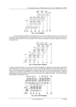
When we multiply binary numbers there are lots of zeros, whenever any of the multiplicand bit is zero
and it gets multiplied by any bit it produces zero . In Braun’s multiplier the resultant zeros are added and the
corresponding full adders work and consume power. So Bypass techniques are employed to deactivate the full
adders when multiplying with zeros. This will reduce the power consumption.
II. Previous Work And Related Research
The architecture view of a 4*4 Standard Braun multiplier is as shown in Fig.:1.Braun Multiplier is a
simple parallel multiplier generally called as CSM (carry save multiplier). This parallel multiplier is used to
perform the unsigned bit multiplication. The Braun multiplier structure makes of the array of array of AND
gates and full adders. To implement the n*n multiplier n(n-1) full adders and n2AND gate are required[2]. The
delay introduced by the Braun’s multiplier depends on the delay of the full adders and also on the delay of the
final adder in the last stage which is a ripple carry adder. The dynamic power dissipation of the multiplier
resulting from the switching activities can be reduced via bypassing techniques like Row bypassing, column
bypassing and Reversible Logic techniques [3].](https://image.slidesharecdn.com/l01536470-150114045911-conversion-gate01/85/VLSI-Implementation-of-High-Speed-Low-Power-Multiplier-in-FPGA-1-320.jpg)
![IOSR Journal of Computer Engineering (IOSR-JCE)
e-ISSN: 2278-0661, p- ISSN: 2278-8727Volume 15, Issue 3 (Nov. - Dec. 2013), PP 64-70
www.iosrjournals.org
www.iosrjournals.org 64 | Page
VLSI Implementation of High Speed & Low Power Multiplier in
FPGA
Prashant Kumar Sahu 1
, Asst. Prof. Nitin Meena ,
2
Prof. Shweta Singh3
1,2,3
(EC, IES College, Bhopal / RGPV, India)
Abstract : We known that different multipliers consume most of the power in DSP computations, FIR filters.
Hence, it is very important factor for modern DSP systems to built low-power multipliers to minimize the power
dissipation. In this paper, we presents high speed & low power Row Column bypass multiplier design
methodology that inserts more number of zeros in the multiplicand thereby bypass the number of zero in row &
Column as well as reduce power consumption. The bypassing of zero activity of the component used in the
process of multiplication, depends on the input bit data. This means if the input bit data is zero, corresponding
row and column of adders need not be addition & transfer bit in next row and column adder circuit. If
multiplicand having more zeros, higher power reduction can be achieved. At last stage of Row & column bypass
multiplier having ripple carry adder which are increase time to generate carry bit to transfer next adder
circuit. To reduce this problem by using Carry bypass adder in place of ripple carry adder, then new
modification of Row &column multiplier having high speed in comparison to simple row & column bypass
multiplier, , the experimental results show that our proposed multiplier reduces power dissipation & High
speed overhead on the average for 4x4, 8x8 and 16x16 multiplier.
Keywords: Low Power, Row & Column bypass Multiplier, Carry bypassing techniques, FPGA, Xilinx .
I. INTRODUCTION
Multipliers are key components of many high performance systems such as filters, microprocessors,
digital signal processors, etc. A system’s capability is generally determined by the performance of the multiplier
because the multiplier is generally the slowest element in the system. Multiplier required more hardware
resources and processing time then addition and subtraction. In fact 8.74% of all instructions in a typical
processing unit is a multiplier. In computer a typical central processing unit devotes a considerable amount of
processing time in arithmetic operation, particularly multiplication operation. Multiplication is an important
fundamental arithmetic operation. Multiplication based operation such as multiply and accumulate (MAC) are
currently implemented in many digital signal processing application such as convolution, Fast Fourier
Transform (FFT), Filtering and in microprocessor in its arithmetic and logic unit. Since multiplication
dominants the execution time of most DSP application, there is a need to high speed multiplier. Currently
multiplication time is still that dominant factor in determining the instruction cycle time of DSP chip. The
multiplier is fairly large block in of computing system.
In the past many novel ideas for multiplier have been proposed to achieve high performance. Higher
throughput arithmetic operations are important to achieve the desire performance in many real time signal and
image processing application. On of the key arithmetic operation in such application is multiplication and the
development of fast multiplier circuit has been a subject of interest over decades. Reducing the delay and power
consumption is very essential requirement for many applications.
When we multiply binary numbers there are lots of zeros, whenever any of the multiplicand bit is zero
and it gets multiplied by any bit it produces zero . In Braun’s multiplier the resultant zeros are added and the
corresponding full adders work and consume power. So Bypass techniques are employed to deactivate the full
adders when multiplying with zeros. This will reduce the power consumption.
II. Previous Work And Related Research
The architecture view of a 4*4 Standard Braun multiplier is as shown in Fig.:1.Braun Multiplier is a
simple parallel multiplier generally called as CSM (carry save multiplier). This parallel multiplier is used to
perform the unsigned bit multiplication. The Braun multiplier structure makes of the array of array of AND
gates and full adders. To implement the n*n multiplier n(n-1) full adders and n2AND gate are required[2]. The
delay introduced by the Braun’s multiplier depends on the delay of the full adders and also on the delay of the
final adder in the last stage which is a ripple carry adder. The dynamic power dissipation of the multiplier
resulting from the switching activities can be reduced via bypassing techniques like Row bypassing, column
bypassing and Reversible Logic techniques [3].](https://image.slidesharecdn.com/l01536470-150114045911-conversion-gate01/75/VLSI-Implementation-of-High-Speed-Low-Power-Multiplier-in-FPGA-1-2048.jpg)
![Vlsi Implimentation of High Speed & Low Power Multiplier in FPGA
www.iosrjournals.org 70 | Page
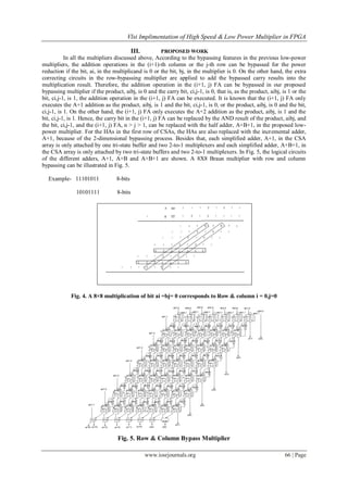
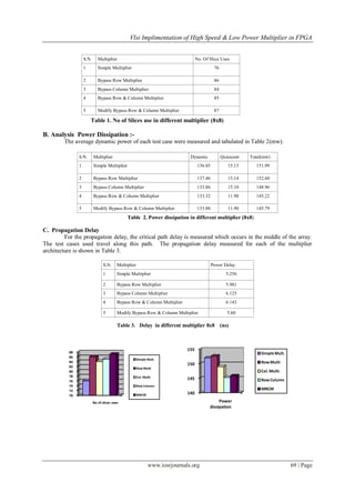
V. Conclusion
We have introduced low-power multiplier design and High speed bypass method in this paper. Our
proposed modify Row & Column Bypass multipliers are useful for all multipliers. To reduce the power and
increase speed, From the obtained results in Xilinx and Cadence, it can be concluded that if the multiplier is to
be used for high – speed applications, then a Carry Bypass adder can be used with the multiplier design but the
area as well as the dynamic power increases.
Vi. Future Work
In this paper, the proposed work has been done for 8*8 and 16*16 bit unsigned multipliers. The
bypassing techniques with the architectural modifications can also be applied to signed array multiplier
architectures. Proposed multiplier using conventional Adder (Full Adder) can be replaced by new Fast Adder &
change of Multiplication algorithm. In this paper, the proposed work has been done for using tri state buffer
which having floating point problem ,can be modify by using transistors.
References
[1] Prashant kumar Sahu and Asst. Prof Nitin Meena, “Comparative Study Of Different Multiplier Architecture”, IJETT, Volume 4
Issue ,pp. 4293,10- Oct 2013.
[2] M. C. Wen, S. J. Wang and Y. M. Lin, “Low power parallel multiplier with column bypassing,“ IEEE International Symposium on
Circuits and Systems, 2005.
[3] Ming-Chen Wen, Sying-Jyan Wang, and Yen-Nan Lin, “Low power parallel multiplier with column-bypassing,” IEEE International
Symposium on Circuits and Systems, ISCAS, vol. 2, pp.1638-1641, May 2005.
[4] J. Ohban, V. G. Moshnyaga, K. Inoue, “Multiplier energy reduction through Bypassing of partial products”, IEEE Asia-Pacific
Conference on Circuits and Systems, pp.13-17, 2002.
[5] Chang-Young Han, Hyoung-Joon Park, and Lee-Sup Kim, “A low-power array multiplier using separated multiplication
technique,” IEEE Transactions on Circuits and Systems II: Analog and Digital Signal Processing, Volume 48, Issue 9, pp.866-871,
Sept. 2001.
[6] B. Parhami, Computer Arithmetic: Algorithms and Hardware Designs, Oxford University Press, 2000.
[7] C. R. Baugh and B. A. Wooley, ”A two’s complement parallel array multiplication algorithm,” IEEE Trans. Comput., vol. C-22, pp.
1045-1047, Dec. 1973.
.
4.5
5
5.5
6
6.5
POWER DELAY
SimpleMult.
Row Multi
Col. Multi.
Row Column
MRCM](https://image.slidesharecdn.com/l01536470-150114045911-conversion-gate01/85/VLSI-Implementation-of-High-Speed-Low-Power-Multiplier-in-FPGA-7-320.jpg)

This paper presents a methodology for designing a high-speed and low-power row-column bypass multiplier suitable for FPGA implementation, focusing on minimizing power consumption by bypassing operations involving zeros in the input data. It proposes using carry bypass adders to replace traditional ripple carry adders in order to enhance speed while reducing dissipation in various multiplier configurations. Experimental results demonstrate that the proposed design significantly lowers power usage and improves performance in 4x4, 8x8, and 16x16 multipliers.