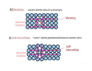
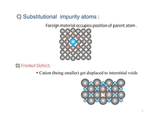
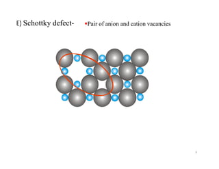
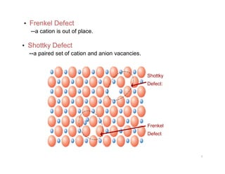
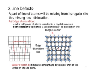
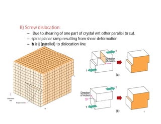
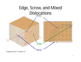
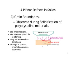
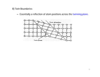
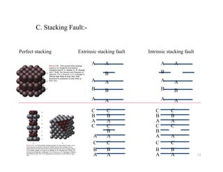
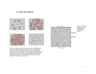
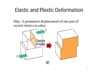
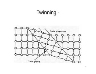
Material Science
Imperfections In Crystals
By
Sandip Thorat
Mechanical Engg. Department
SRES, Sanjivani College of Engineering,
Kopargaon. (MS) 423603
1
Imperfections In Crystal –
1. Lattice Vibrations or Phonons or volume defect: –
- Vibration of atoms @ their mean position
-Frequency of vibration depends on temp.
-Specific heat and electrical resistance of
material.
2
2. Point Defect or zero dimensional Defect:-
-Due to Vibration and Temp braking of bonds
-Atoms are free from their lattice sites.
• The simplest of the point defect is a vacancy,
or vacant lattice site.
• All crystalline solids contain vacancies.
3
A)Vacancy: vacant atomic sites in a structure.
B) Self-Interstitials: -"extra" atoms positioned between atomic sites.
Vacancy
distortion
of planes
self-
interstitial
distortion
of planes
4
C) Substitutional impurity atoms :
Foreign material occupies position of parent atom .
D) Frenkel Defect:
 Cation (being smaller) get displaced to interstitial voids
5
E) Schottky defect- Pair of anion and cation vacancies
6
• Frenkel Defect
--a cation is out of place.
• Shottky Defect
--a paired set of cation and anion vacancies.
Shottky
Defect:
Frenkel
Defect
7
A part of line of atoms will be missing from its regular site
this missing row –dislocation.
A) Edge dislocation:
- extra half-plane of atoms inserted in a crystal structure
b (the berger’s vector) is  (perpendicular) to dislocation line
3.Line Defects-
Burger’s vector, b: It indicates amount and direction of shift of the
lattice on the slip plane.
8
B) Screw dislocation:
– Due to shearing of one part of crystal wrt other parallel to cut.
– spiral planar ramp resulting from shear deformation
– b is  (parallel) to dislocation line
9
10
Edge, Screw, and Mixed
Dislocations
Adapted from Fig. 4.5, Callister 7e.
Edge
Screw
Mixed
A) Grain Boundaries-
– Observed during Solidification of
polycrystaline materials.
4.Planar Defects in Solids
grain boundary
surface groove
polished surface
(a)
• are imperfections,
• are more susceptible
to etching,
• may be revealed as
dark lines,
• change in crystal
orientation across
boundary.
11
B) Twin Boundaries-
– Essentially a reflection of atom positions across the twinning plane.
12
C. Stacking Fault:-
Extrinsic stacking fault Intrinsic stacking faultPerfect stacking
B
A
A
B
AA
A
B
A
B
A
A
B
AA
A
B
A
B
A
A
B
AA
A
B
A
CC
C
B
C
C
B
C
B
A
B
AA
A
B
CC
C
B
C
B
CC
AA 13
2. Grain Boundaries
14
Elastic and Plastic Deformation
Slip:- A permanent displacement of one part of
crystal relative to other.
15
Twinning:-
16

Crystal imperfections

  • 1.
    Material Science Imperfections InCrystals By Sandip Thorat Mechanical Engg. Department SRES, Sanjivani College of Engineering, Kopargaon. (MS) 423603 1
  • 2.
    Imperfections In Crystal– 1. Lattice Vibrations or Phonons or volume defect: – - Vibration of atoms @ their mean position -Frequency of vibration depends on temp. -Specific heat and electrical resistance of material. 2
  • 3.
    2. Point Defector zero dimensional Defect:- -Due to Vibration and Temp braking of bonds -Atoms are free from their lattice sites. • The simplest of the point defect is a vacancy, or vacant lattice site. • All crystalline solids contain vacancies. 3
  • 4.
    A)Vacancy: vacant atomicsites in a structure. B) Self-Interstitials: -"extra" atoms positioned between atomic sites. Vacancy distortion of planes self- interstitial distortion of planes 4
  • 5.
    C) Substitutional impurityatoms : Foreign material occupies position of parent atom . D) Frenkel Defect:  Cation (being smaller) get displaced to interstitial voids 5
  • 6.
    E) Schottky defect-Pair of anion and cation vacancies 6
  • 7.
    • Frenkel Defect --acation is out of place. • Shottky Defect --a paired set of cation and anion vacancies. Shottky Defect: Frenkel Defect 7
  • 8.
    A part ofline of atoms will be missing from its regular site this missing row –dislocation. A) Edge dislocation: - extra half-plane of atoms inserted in a crystal structure b (the berger’s vector) is  (perpendicular) to dislocation line 3.Line Defects- Burger’s vector, b: It indicates amount and direction of shift of the lattice on the slip plane. 8
  • 9.
    B) Screw dislocation: –Due to shearing of one part of crystal wrt other parallel to cut. – spiral planar ramp resulting from shear deformation – b is  (parallel) to dislocation line 9
  • 10.
    10 Edge, Screw, andMixed Dislocations Adapted from Fig. 4.5, Callister 7e. Edge Screw Mixed
  • 11.
    A) Grain Boundaries- –Observed during Solidification of polycrystaline materials. 4.Planar Defects in Solids grain boundary surface groove polished surface (a) • are imperfections, • are more susceptible to etching, • may be revealed as dark lines, • change in crystal orientation across boundary. 11
  • 12.
    B) Twin Boundaries- –Essentially a reflection of atom positions across the twinning plane. 12
  • 13.
    C. Stacking Fault:- Extrinsicstacking fault Intrinsic stacking faultPerfect stacking B A A B AA A B A B A A B AA A B A B A A B AA A B A CC C B C C B C B A B AA A B CC C B C B CC AA 13
  • 14.
  • 15.
    Elastic and PlasticDeformation Slip:- A permanent displacement of one part of crystal relative to other. 15
  • 16.