Downloaded 284 times

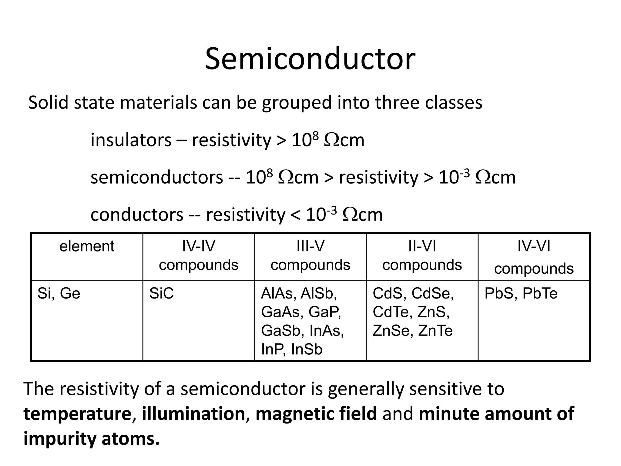
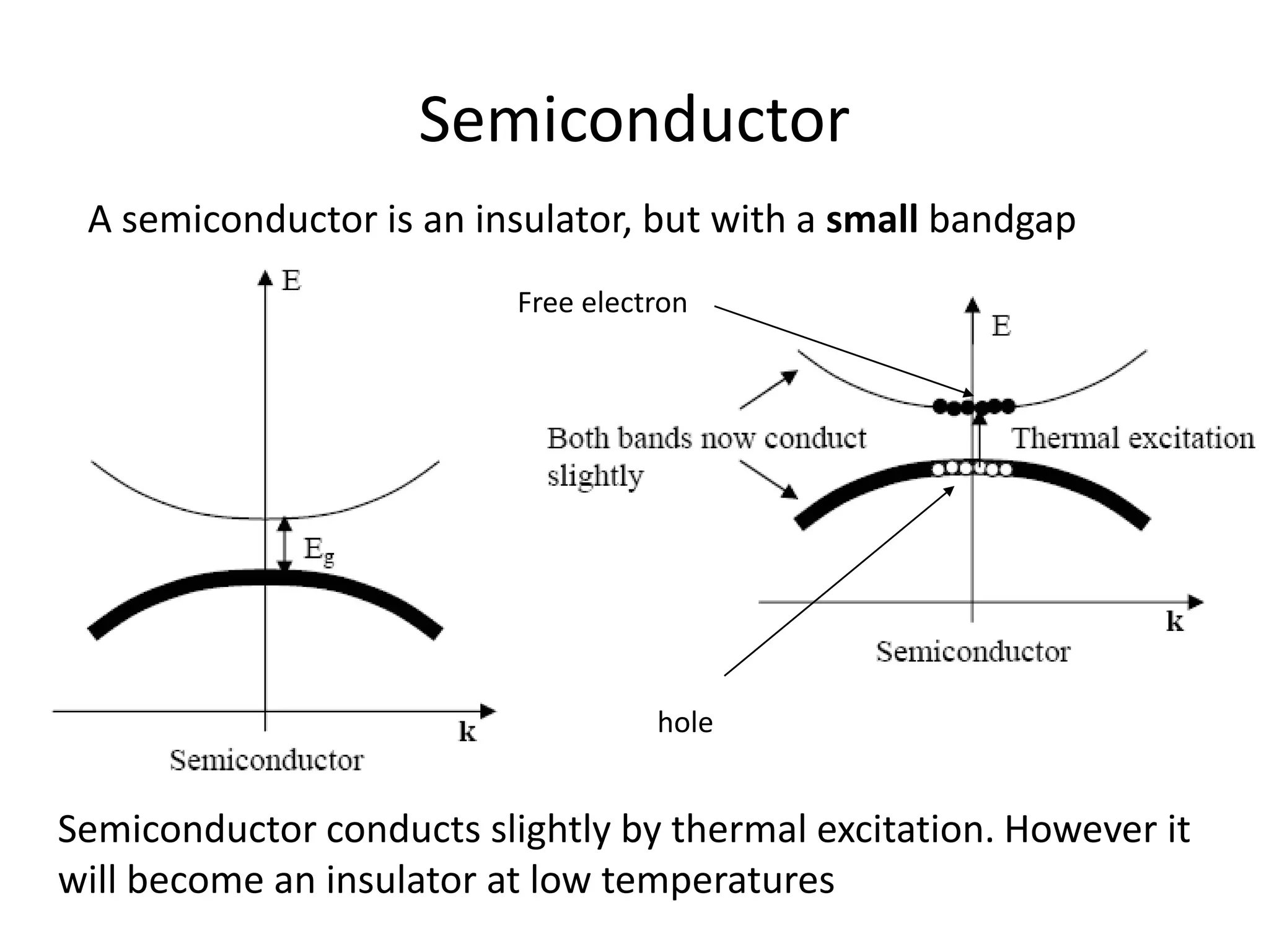


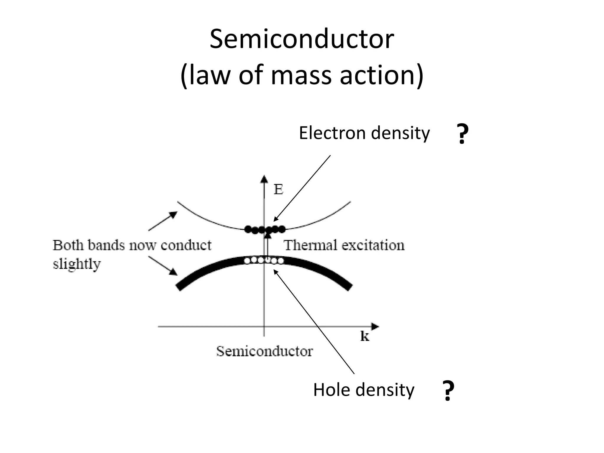


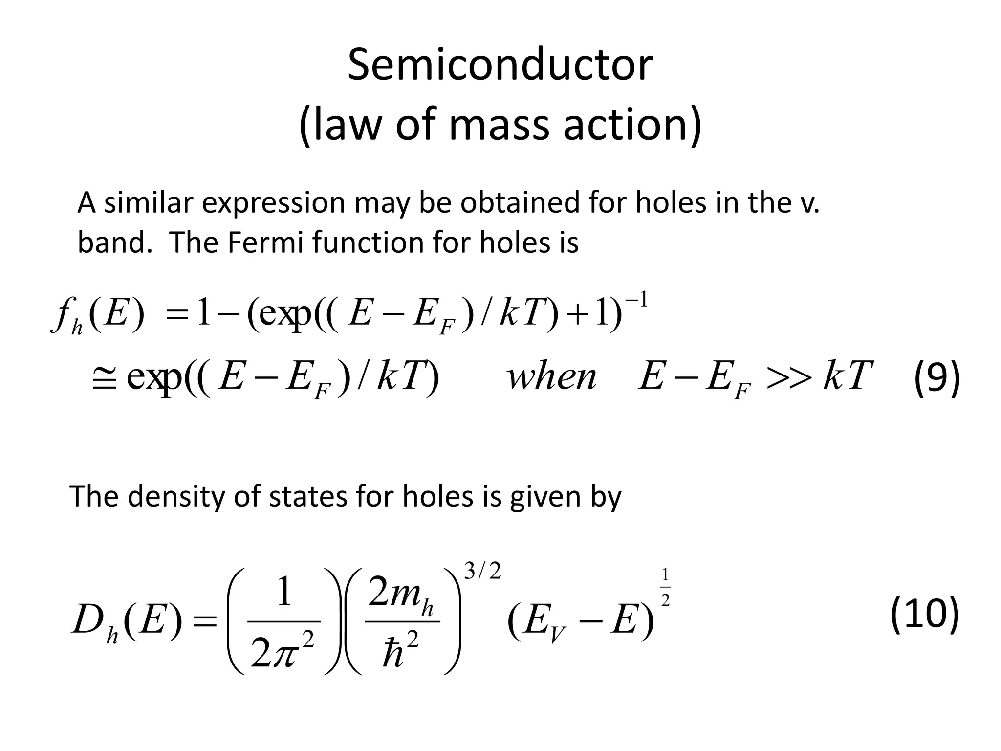


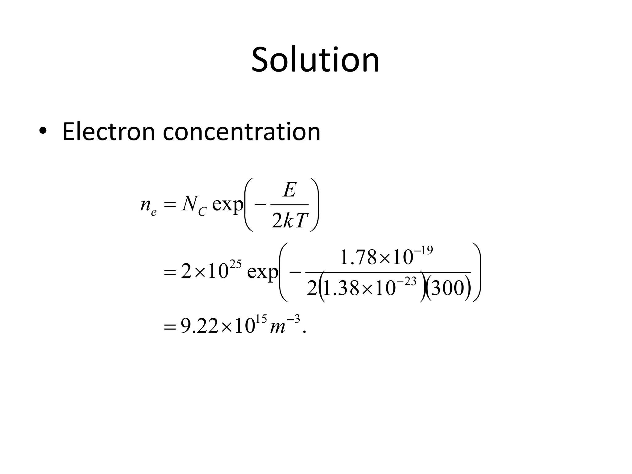

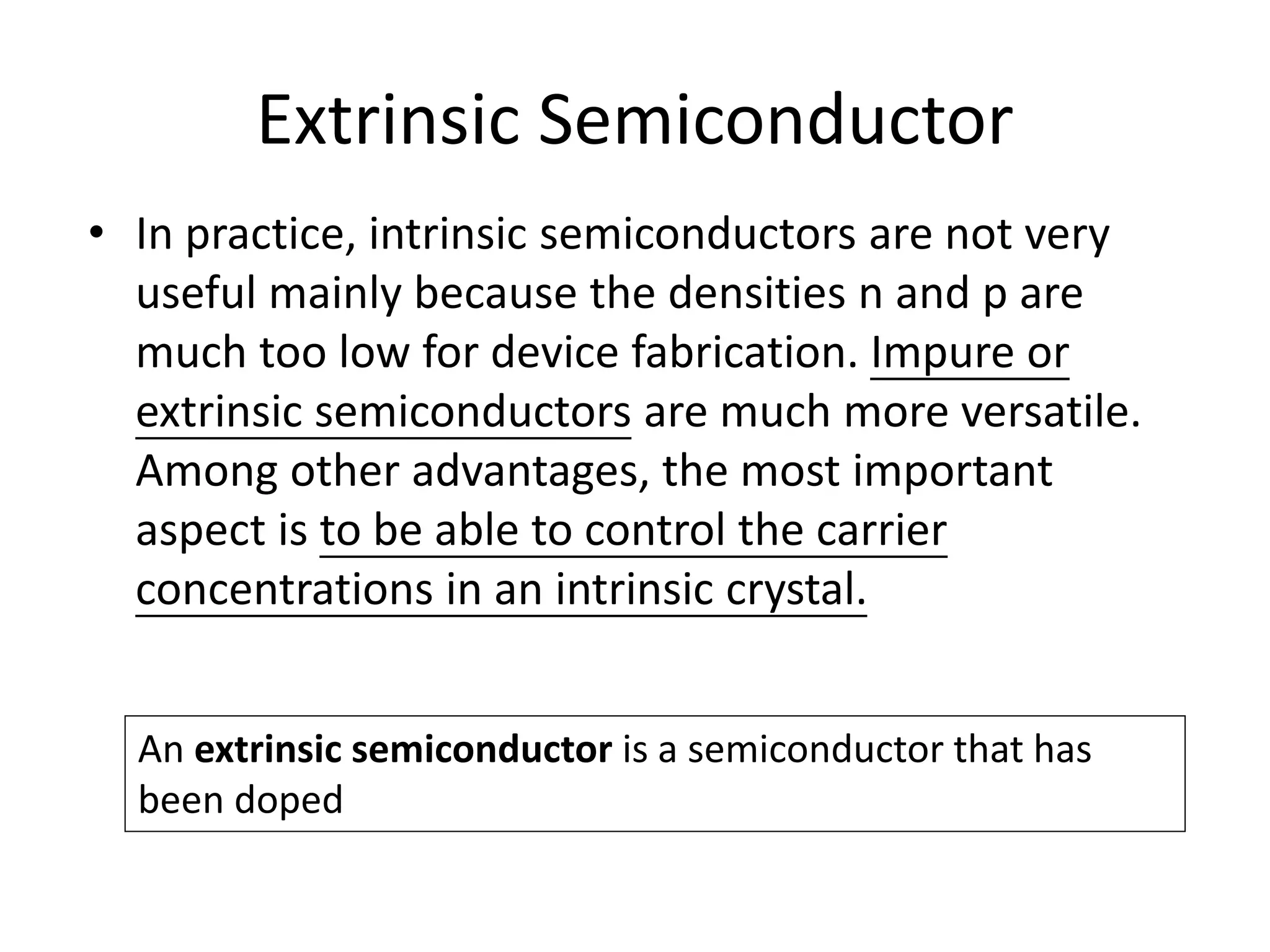


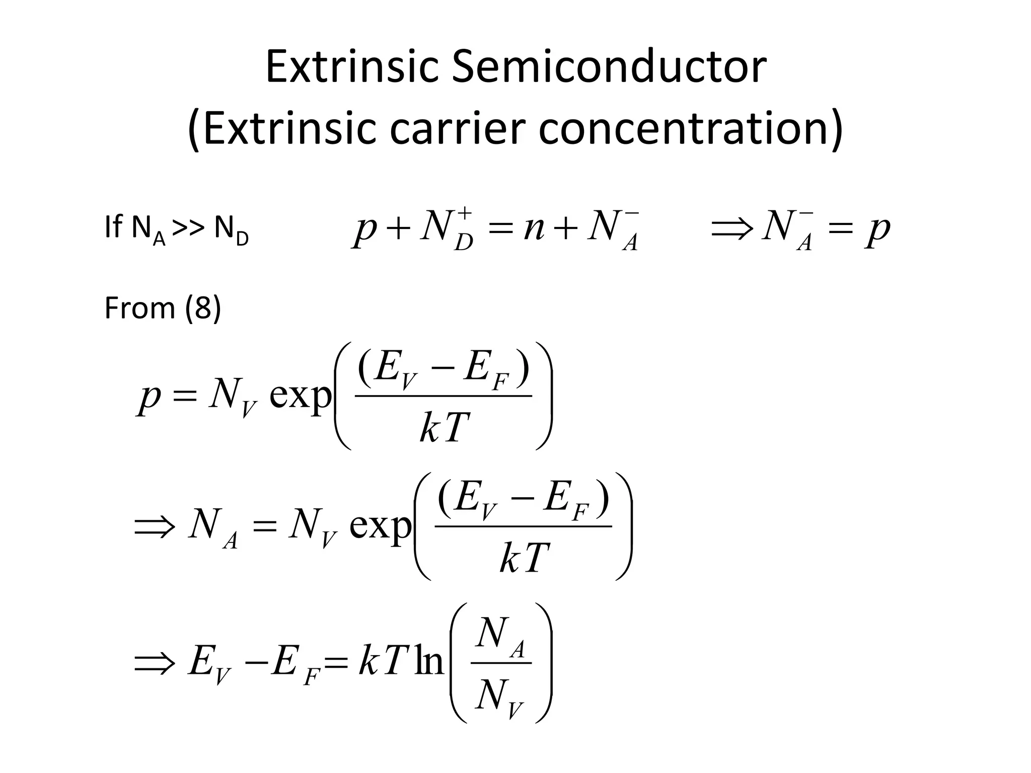


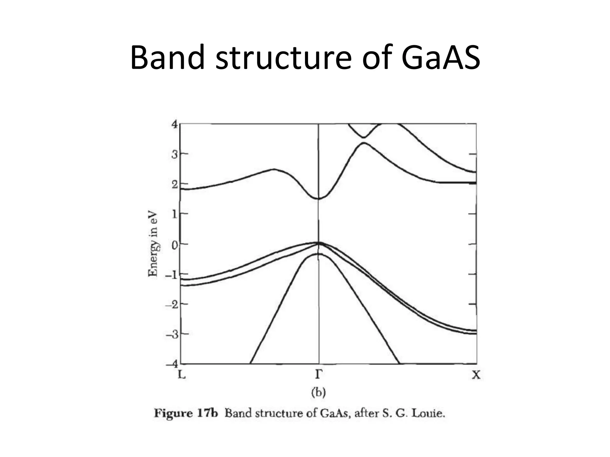

This document discusses semiconductors and their properties. It begins by defining semiconductors as materials with resistivity between insulators and conductors. It then discusses several key points: - Semiconductor resistivity is sensitive to temperature, illumination, magnetic fields, and impurities. - Common semiconductor materials include silicon, germanium, and various compound semiconductors. - Semiconductors have a small bandgap that allows slight conductivity through thermal excitation of electrons. - The bandgap can be measured through optical absorption and determines many material properties. - Carrier concentrations in intrinsic and extrinsic semiconductors are described through concepts like the density of states, Fer