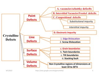
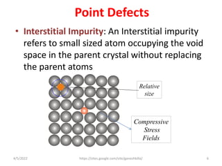
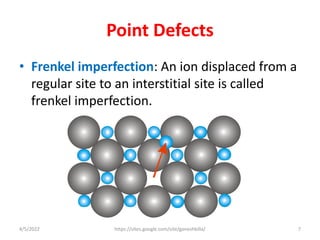
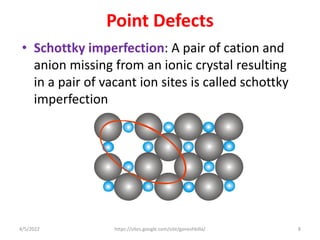
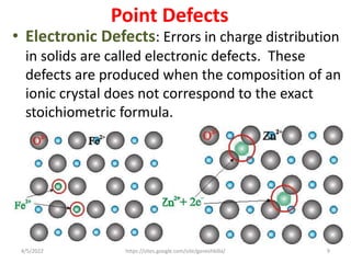
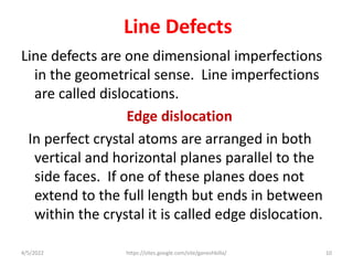
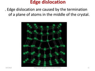
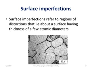
SlideShare a Scribd company logo
Defects in crystals
4/5/2022 1
https://sites.google.com/site/ganeshbilla/
Imperfections in crystals
Crystalline imperfections can be classified
on the basis of their geometry as follows
4/5/2022 2
https://sites.google.com/site/ganeshbilla/
A. vacancies/schottky defecfts
B. Interstitial Vacancies/Frenkel defecfts
C. Compositional defecfts
Interstitial impurity
Substitutional impurity
D. Electronic impurity
Point
Defects
Line
Defects
Surface
Defects
Volume
Defects
1. Edge Dislocation
2. Screw Dislocation
a. Grain boundaries
b. Twin boundaries
c. Tilt boundaries
d. Stacking fault
Non Crystalline regions of dimensions at
least 10 to 30°A
Crystalline
Defects
4/5/2022 3
https://sites.google.com/site/ganeshbilla/
Point Defects
• Vacancy: A Vacancy refers to an atomic site
from where the atom is missing.
Tensile Stress
Fields ?
4/5/2022 4
https://sites.google.com/site/ganeshbilla/
Point Defects
• Substitutional impurity: A Substitutional
impurity refers to a foreign atom that has
replaced a parent atom.
Tensile Stress
Fields
Compressive stress
fields
4/5/2022 5
https://sites.google.com/site/ganeshbilla/
Point Defects
• Interstitial Impurity: An Interstitial impurity
refers to small sized atom occupying the void
space in the parent crystal without replacing
the parent atoms
Compressive
Stress
Fields
Relative
size
4/5/2022 6
https://sites.google.com/site/ganeshbilla/
Point Defects
• Frenkel imperfection: An ion displaced from a
regular site to an interstitial site is called
frenkel imperfection.
4/5/2022 7
https://sites.google.com/site/ganeshbilla/
Point Defects
• Schottky imperfection: A pair of cation and
anion missing from an ionic crystal resulting
in a pair of vacant ion sites is called schottky
imperfection
4/5/2022 8
https://sites.google.com/site/ganeshbilla/
Point Defects
• Electronic Defects: Errors in charge distribution
in solids are called electronic defects. These
defects are produced when the composition of an
ionic crystal does not correspond to the exact
stoichiometric formula.
4/5/2022 9
https://sites.google.com/site/ganeshbilla/
Line Defects
Line defects are one dimensional imperfections
in the geometrical sense. Line imperfections
are called dislocations.
Edge dislocation
In perfect crystal atoms are arranged in both
vertical and horizontal planes parallel to the
side faces. If one of these planes does not
extend to the full length but ends in between
within the crystal it is called edge dislocation.
4/5/2022 10
https://sites.google.com/site/ganeshbilla/
Edge dislocation
. Edge dislocation are caused by the termination
of a plane of atoms in the middle of the crystal.
4/5/2022 11
https://sites.google.com/site/ganeshbilla/
4/5/2022 12
https://sites.google.com/site/ganeshbilla/
Burger’s Vector
• The presence of dislocation results in lattice
strain (distortion). The direction and
magnitude of such distortion is expressed in
terms of a Burger’s vector.
Or
The magnitude and the direction of the
displacement are defined by a vector called
the burger vector.
4/5/2022 13
https://sites.google.com/site/ganeshbilla/
4
3 3
4
4
3 3
4
Above: Burger’s circuit for dislocation-free material.
To Right: Do same with dislocation and end up
“past” starting point.
Vector b = distance to get back to curcuit.
note “compressed bonds” and “elongated bonds.”
4/5/2022 14
https://sites.google.com/site/ganeshbilla/
• The Burgers vector(b) is perpendicular to the
edge dislocation line
• The Burgers vector(b) is parallel to the screw
dislocation line.
Screw Dislocation
Screw dislocation results from a displacement
of the atoms in one part of a crystal relative to
the rest of the crystal forming a spiral ramp
around the dislocation line.
4/5/2022 15
https://sites.google.com/site/ganeshbilla/
Screw
Dislocation Slip Planes
Slip Direction
4/5/2022 16
https://sites.google.com/site/ganeshbilla/
Surface imperfections
• Surface imperfections refer to regions of
distortions that lie about a surface having
thickness of a few atomic diameters
4/5/2022 17
https://sites.google.com/site/ganeshbilla/
Surface imperfections
• Grain Boundaries (or) Crystal Boundary
At the interface between two crystals
randomly oriented the atoms held in between
are attracted by crystals on either side and
depending on the forces the atoms occupy
equilibrium positions. This distorted region of
a few atomic diameter thickness is called grain
boundary.
4/5/2022 18
https://sites.google.com/site/ganeshbilla/
Surface imperfections
• The orientation difference is usually greater
than 10-15°. For this reason the grain
boundaries are also known as high angle
boundaries.
• When the orientation difference between two
crystals is less than 10° the distortion in the
boundary is not so drastic. They are called
low angle boundaries.
4/5/2022 19
https://sites.google.com/site/ganeshbilla/
Surface imperfections
• The sub grain boundaries are of two types
they are
1. Tilt boundaries
2. Twist boundaries.
• An array of edge dislocations is called tilt
boundary
• A cross grid of screw dislocation is called twist
boundaries.
4/5/2022 20
https://sites.google.com/site/ganeshbilla/
4/5/2022 21
https://sites.google.com/site/ganeshbilla/
Tilt
boundaries
Twist
boundaries
Twin Boundaries
A twin boundary happens when
the crystals on either side of a
plane are mirror images of each
other. Two single crystal sections
are miss oriented but joined
together such that one plane is a
mirror image of the other. The
boundary common to the two
planes is a twin boundary. They
are formed during the growth of
crystal
The boundary between the
twinned crystals will be a single
plane of atoms.
4/5/2022 22
https://sites.google.com/site/ganeshbilla/
Stacking Faults
• Stacking faults are planar surface imperfections caused by
fault in the staking sequence of atomic planes in crystals
• In FCC crystal we have three different stacking layers
ABC while in HCP stacking we have only two different
layers BC hence when FCC crystal grows we have the
stacking as
………ABCABCABCABC……
While growing if the plane A indicated by arrow above
missing then we get the sequence
………ABCABCBCABC……
Thus we find that the stacking in the missing region be comes
HCP. This thin region is a surface imperfection and is
called a stocking fault.
4/5/2022 https://sites.google.com/site/ganeshbilla/ 23
Volume Defects
• Presence of a large vacancy (crakes) or void
such as clusters of atoms missing is also
considered as a volume defect. While crystal
is grown there is every possibility of inclusion
of non-crystalline regions of dimensions of at
least 10 to 30°A. This is also called Volume
imperfection.
4/5/2022 24
https://sites.google.com/site/ganeshbilla/
4/5/2022 25
https://sites.google.com/site/ganeshbilla/

More Related Content

What's hot

Imperfections in
Imperfections inImperfections in
Imperfections in
Mayur Bagale
 
Crystal defects
Crystal defectsCrystal defects
Crystal defects
amalajanet
 
Frankel and schottky defects
Frankel and schottky defectsFrankel and schottky defects
Frankel and schottky defects
Gurpreet Singh
 
Defects in crystalline materials
Defects in crystalline materialsDefects in crystalline materials
Defects in crystalline materials
onlinemetallurgy.com
 
Defects in crystal
Defects in crystalDefects in crystal
Defects in crystal
Vidhya1980
 
Solidification of alloys
Solidification of alloysSolidification of alloys
Solidification of alloys
shivammanu
 
Crystal defects pk cnu
Crystal defects pk cnuCrystal defects pk cnu
Crystal defects pk cnu
Kedhareswara Sairam Pasupuleti
 
Metallurgy School 1: Dislocation
Metallurgy School 1: DislocationMetallurgy School 1: Dislocation
Metallurgy School 1: Dislocation
masusc
 
Crystal Defects
Crystal DefectsCrystal Defects
Crystal Defects
Vikash Prasad
 
Solid solution
Solid solutionSolid solution
Solid solution
Ratnadeepsinh Jadeja
 
Point defects
Point defectsPoint defects
Point defects
babar15me21
 
Crystal defect and significance
Crystal defect and significanceCrystal defect and significance
Crystal defect and significance
Shivam Jain
 
Defects
DefectsDefects
Defects
Mayur Bagale
 
Line defects & planes
Line defects & planesLine defects & planes
Line defects & planes
onlinemetallurgy.com
 
Crystal Structure, BCC ,FCC,HCP
Crystal Structure, BCC ,FCC,HCPCrystal Structure, BCC ,FCC,HCP
Crystal Structure, BCC ,FCC,HCP
BSMRSTU
 
Defects in materials
Defects in materialsDefects in materials
Defects in materials
srinivasreddy gavinolla
 
6 defects
6 defects6 defects
6 defects
Sattar kayani
 
Wet or electrochemical corrosion
Wet or electrochemical corrosionWet or electrochemical corrosion
Wet or electrochemical corrosion
Sarala Prasanna Pattanaik
 
Crystal defects
Crystal defectsCrystal defects
Crystal defects
MehakTariq5
 
Packing Factor
Packing Factor Packing Factor
Packing Factor
Gulfam Hussain
 

What's hot (20)

Imperfections in
Imperfections inImperfections in
Imperfections in
 
Crystal defects
Crystal defectsCrystal defects
Crystal defects
 
Frankel and schottky defects
Frankel and schottky defectsFrankel and schottky defects
Frankel and schottky defects
 
Defects in crystalline materials
Defects in crystalline materialsDefects in crystalline materials
Defects in crystalline materials
 
Defects in crystal
Defects in crystalDefects in crystal
Defects in crystal
 
Solidification of alloys
Solidification of alloysSolidification of alloys
Solidification of alloys
 
Crystal defects pk cnu
Crystal defects pk cnuCrystal defects pk cnu
Crystal defects pk cnu
 
Metallurgy School 1: Dislocation
Metallurgy School 1: DislocationMetallurgy School 1: Dislocation
Metallurgy School 1: Dislocation
 
Crystal Defects
Crystal DefectsCrystal Defects
Crystal Defects
 
Solid solution
Solid solutionSolid solution
Solid solution
 
Point defects
Point defectsPoint defects
Point defects
 
Crystal defect and significance
Crystal defect and significanceCrystal defect and significance
Crystal defect and significance
 
Defects
DefectsDefects
Defects
 
Line defects & planes
Line defects & planesLine defects & planes
Line defects & planes
 
Crystal Structure, BCC ,FCC,HCP
Crystal Structure, BCC ,FCC,HCPCrystal Structure, BCC ,FCC,HCP
Crystal Structure, BCC ,FCC,HCP
 
Defects in materials
Defects in materialsDefects in materials
Defects in materials
 
6 defects
6 defects6 defects
6 defects
 
Wet or electrochemical corrosion
Wet or electrochemical corrosionWet or electrochemical corrosion
Wet or electrochemical corrosion
 
Crystal defects
Crystal defectsCrystal defects
Crystal defects
 
Packing Factor
Packing Factor Packing Factor
Packing Factor
 

Similar to Defects in crystals

Lecture presentation
Lecture presentationLecture presentation
Lecture presentation
R G Sanjay Prakash
 
Presentation of deformation behaviour of materials
Presentation of deformation behaviour of materialsPresentation of deformation behaviour of materials
Presentation of deformation behaviour of materials
chotlalvarma
 
Material science and Metallurgy Lecture 10.pptx
Material science and Metallurgy Lecture 10.pptxMaterial science and Metallurgy Lecture 10.pptx
Material science and Metallurgy Lecture 10.pptx
sagar642508
 
Crystal imperfections
Crystal imperfections Crystal imperfections
Crystal imperfections
Dr. Sandip Thorat
 
6 - Lattice defects.pdf
6 - Lattice defects.pdf6 - Lattice defects.pdf
6 - Lattice defects.pdf
Praveen Kumar
 
Subject Defects in Solids physics presentation
Subject Defects in Solids physics  presentationSubject Defects in Solids physics  presentation
Subject Defects in Solids physics presentation
trueangel2022
 
Deformation and kink bads
Deformation and kink badsDeformation and kink bads
Ch04 sent fall2016
Ch04 sent fall2016Ch04 sent fall2016
Ch04 sent fall2016
Savanna Holt
 
MATERIALS-ENGG-UNIT- 2.pptx
MATERIALS-ENGG-UNIT- 2.pptxMATERIALS-ENGG-UNIT- 2.pptx
MATERIALS-ENGG-UNIT- 2.pptx
PRASANNA NAGASAI BELLAMKONDA
 

Similar to Defects in crystals (9)

Lecture presentation
Lecture presentationLecture presentation
Lecture presentation
 
Presentation of deformation behaviour of materials
Presentation of deformation behaviour of materialsPresentation of deformation behaviour of materials
Presentation of deformation behaviour of materials
 
Material science and Metallurgy Lecture 10.pptx
Material science and Metallurgy Lecture 10.pptxMaterial science and Metallurgy Lecture 10.pptx
Material science and Metallurgy Lecture 10.pptx
 
Crystal imperfections
Crystal imperfections Crystal imperfections
Crystal imperfections
 
6 - Lattice defects.pdf
6 - Lattice defects.pdf6 - Lattice defects.pdf
6 - Lattice defects.pdf
 
Subject Defects in Solids physics presentation
Subject Defects in Solids physics  presentationSubject Defects in Solids physics  presentation
Subject Defects in Solids physics presentation
 
Deformation and kink bads
Deformation and kink badsDeformation and kink bads
Deformation and kink bads
 
Ch04 sent fall2016
Ch04 sent fall2016Ch04 sent fall2016
Ch04 sent fall2016
 
MATERIALS-ENGG-UNIT- 2.pptx
MATERIALS-ENGG-UNIT- 2.pptxMATERIALS-ENGG-UNIT- 2.pptx
MATERIALS-ENGG-UNIT- 2.pptx
 

More from kveerabhadrarao1

Engineering. physics lab manual 2014-15-05.03.2015(1)
Engineering. physics lab manual 2014-15-05.03.2015(1)Engineering. physics lab manual 2014-15-05.03.2015(1)
Engineering. physics lab manual 2014-15-05.03.2015(1)
kveerabhadrarao1
 
Final ep course_file-10.03
Final ep course_file-10.03Final ep course_file-10.03
Final ep course_file-10.03
kveerabhadrarao1
 
LED
LEDLED
LCD
LCDLCD
Engineering physics lab manual
Engineering physics lab manualEngineering physics lab manual
Engineering physics lab manual
kveerabhadrarao1
 
Elementsofstatisticalmechanics
ElementsofstatisticalmechanicsElementsofstatisticalmechanics
Elementsofstatisticalmechanics
kveerabhadrarao1
 
Dielectric properties[read only]
Dielectric properties[read only]Dielectric properties[read only]
Dielectric properties[read only]
kveerabhadrarao1
 
Nanomaterials
NanomaterialsNanomaterials
Nanomaterials
kveerabhadrarao1
 
Wavemechanics
WavemechanicsWavemechanics
Wavemechanics
kveerabhadrarao1
 
Magnetic materials
Magnetic materialsMagnetic materials
Magnetic materials
kveerabhadrarao1
 
Laser1
Laser1Laser1
Electromagnetic waves
Electromagnetic wavesElectromagnetic waves
Electromagnetic waves
kveerabhadrarao1
 
Bandtheory of solids
Bandtheory of solidsBandtheory of solids
Bandtheory of solids
kveerabhadrarao1
 
Crystallography
CrystallographyCrystallography
Crystallography
kveerabhadrarao1
 

More from kveerabhadrarao1 (14)

Engineering. physics lab manual 2014-15-05.03.2015(1)
Engineering. physics lab manual 2014-15-05.03.2015(1)Engineering. physics lab manual 2014-15-05.03.2015(1)
Engineering. physics lab manual 2014-15-05.03.2015(1)
 
Final ep course_file-10.03
Final ep course_file-10.03Final ep course_file-10.03
Final ep course_file-10.03
 
LED
LEDLED
LED
 
LCD
LCDLCD
LCD
 
Engineering physics lab manual
Engineering physics lab manualEngineering physics lab manual
Engineering physics lab manual
 
Elementsofstatisticalmechanics
ElementsofstatisticalmechanicsElementsofstatisticalmechanics
Elementsofstatisticalmechanics
 
Dielectric properties[read only]
Dielectric properties[read only]Dielectric properties[read only]
Dielectric properties[read only]
 
Nanomaterials
NanomaterialsNanomaterials
Nanomaterials
 
Wavemechanics
WavemechanicsWavemechanics
Wavemechanics
 
Magnetic materials
Magnetic materialsMagnetic materials
Magnetic materials
 
Laser1
Laser1Laser1
Laser1
 
Electromagnetic waves
Electromagnetic wavesElectromagnetic waves
Electromagnetic waves
 
Bandtheory of solids
Bandtheory of solidsBandtheory of solids
Bandtheory of solids
 
Crystallography
CrystallographyCrystallography
Crystallography
 

Recently uploaded

Generative AI Use cases applications solutions and implementation.pdf
Generative AI Use cases applications solutions and implementation.pdfGenerative AI Use cases applications solutions and implementation.pdf
Generative AI Use cases applications solutions and implementation.pdf
mahaffeycheryld
 
UNIT 4 LINEAR INTEGRATED CIRCUITS-DIGITAL ICS
UNIT 4 LINEAR INTEGRATED CIRCUITS-DIGITAL ICSUNIT 4 LINEAR INTEGRATED CIRCUITS-DIGITAL ICS
UNIT 4 LINEAR INTEGRATED CIRCUITS-DIGITAL ICS
vmspraneeth
 
Blood finder application project report (1).pdf
Blood finder application project report (1).pdfBlood finder application project report (1).pdf
Blood finder application project report (1).pdf
Kamal Acharya
 
Bituminous road construction project based learning report
Bituminous road construction project based learning reportBituminous road construction project based learning report
Bituminous road construction project based learning report
CE19KaushlendraKumar
 
DEEP LEARNING FOR SMART GRID INTRUSION DETECTION: A HYBRID CNN-LSTM-BASED MODEL
DEEP LEARNING FOR SMART GRID INTRUSION DETECTION: A HYBRID CNN-LSTM-BASED MODELDEEP LEARNING FOR SMART GRID INTRUSION DETECTION: A HYBRID CNN-LSTM-BASED MODEL
DEEP LEARNING FOR SMART GRID INTRUSION DETECTION: A HYBRID CNN-LSTM-BASED MODEL
ijaia
 
Ericsson LTE Throughput Troubleshooting Techniques.ppt
Ericsson LTE Throughput Troubleshooting Techniques.pptEricsson LTE Throughput Troubleshooting Techniques.ppt
Ericsson LTE Throughput Troubleshooting Techniques.ppt
wafawafa52
 
Prediction of Electrical Energy Efficiency Using Information on Consumer's Ac...
Prediction of Electrical Energy Efficiency Using Information on Consumer's Ac...Prediction of Electrical Energy Efficiency Using Information on Consumer's Ac...
Prediction of Electrical Energy Efficiency Using Information on Consumer's Ac...
PriyankaKilaniya
 
5G Radio Network Througput Problem Analysis HCIA.pdf
5G Radio Network Througput Problem Analysis HCIA.pdf5G Radio Network Througput Problem Analysis HCIA.pdf
5G Radio Network Througput Problem Analysis HCIA.pdf
AlvianRamadhani5
 
DESIGN AND MANUFACTURE OF CEILING BOARD USING SAWDUST AND WASTE CARTON MATERI...
DESIGN AND MANUFACTURE OF CEILING BOARD USING SAWDUST AND WASTE CARTON MATERI...DESIGN AND MANUFACTURE OF CEILING BOARD USING SAWDUST AND WASTE CARTON MATERI...
DESIGN AND MANUFACTURE OF CEILING BOARD USING SAWDUST AND WASTE CARTON MATERI...
OKORIE1
 
一比一原版(CalArts毕业证)加利福尼亚艺术学院毕业证如何办理
一比一原版(CalArts毕业证)加利福尼亚艺术学院毕业证如何办理一比一原版(CalArts毕业证)加利福尼亚艺术学院毕业证如何办理
一比一原版(CalArts毕业证)加利福尼亚艺术学院毕业证如何办理
ecqow
 
一比一原版(uoft毕业证书)加拿大多伦多大学毕业证如何办理
一比一原版(uoft毕业证书)加拿大多伦多大学毕业证如何办理一比一原版(uoft毕业证书)加拿大多伦多大学毕业证如何办理
一比一原版(uoft毕业证书)加拿大多伦多大学毕业证如何办理
sydezfe
 
一比一原版(uofo毕业证书)美国俄勒冈大学毕业证如何办理
一比一原版(uofo毕业证书)美国俄勒冈大学毕业证如何办理一比一原版(uofo毕业证书)美国俄勒冈大学毕业证如何办理
一比一原版(uofo毕业证书)美国俄勒冈大学毕业证如何办理
upoux
 
smart pill dispenser is designed to improve medication adherence and safety f...
smart pill dispenser is designed to improve medication adherence and safety f...smart pill dispenser is designed to improve medication adherence and safety f...
smart pill dispenser is designed to improve medication adherence and safety f...
um7474492
 
4. Mosca vol I -Fisica-Tipler-5ta-Edicion-Vol-1.pdf
4. Mosca vol I -Fisica-Tipler-5ta-Edicion-Vol-1.pdf4. Mosca vol I -Fisica-Tipler-5ta-Edicion-Vol-1.pdf
4. Mosca vol I -Fisica-Tipler-5ta-Edicion-Vol-1.pdf
Gino153088
 
openshift technical overview - Flow of openshift containerisatoin
openshift technical overview - Flow of openshift containerisatoinopenshift technical overview - Flow of openshift containerisatoin
openshift technical overview - Flow of openshift containerisatoin
snaprevwdev
 
1FIDIC-CONSTRUCTION-CONTRACT-2ND-ED-2017-RED-BOOK.pdf
1FIDIC-CONSTRUCTION-CONTRACT-2ND-ED-2017-RED-BOOK.pdf1FIDIC-CONSTRUCTION-CONTRACT-2ND-ED-2017-RED-BOOK.pdf
1FIDIC-CONSTRUCTION-CONTRACT-2ND-ED-2017-RED-BOOK.pdf
MadhavJungKarki
 
Call For Paper -3rd International Conference on Artificial Intelligence Advan...
Call For Paper -3rd International Conference on Artificial Intelligence Advan...Call For Paper -3rd International Conference on Artificial Intelligence Advan...
Call For Paper -3rd International Conference on Artificial Intelligence Advan...
ijseajournal
 
Zener Diode and its V-I Characteristics and Applications
Zener Diode and its V-I Characteristics and ApplicationsZener Diode and its V-I Characteristics and Applications
Zener Diode and its V-I Characteristics and Applications
Shiny Christobel
 
OOPS_Lab_Manual - programs using C++ programming language
OOPS_Lab_Manual - programs using C++ programming languageOOPS_Lab_Manual - programs using C++ programming language
OOPS_Lab_Manual - programs using C++ programming language
PreethaV16
 
Supermarket Management System Project Report.pdf
Supermarket Management System Project Report.pdfSupermarket Management System Project Report.pdf
Supermarket Management System Project Report.pdf
Kamal Acharya
 

Recently uploaded (20)

Generative AI Use cases applications solutions and implementation.pdf
Generative AI Use cases applications solutions and implementation.pdfGenerative AI Use cases applications solutions and implementation.pdf
Generative AI Use cases applications solutions and implementation.pdf
 
UNIT 4 LINEAR INTEGRATED CIRCUITS-DIGITAL ICS
UNIT 4 LINEAR INTEGRATED CIRCUITS-DIGITAL ICSUNIT 4 LINEAR INTEGRATED CIRCUITS-DIGITAL ICS
UNIT 4 LINEAR INTEGRATED CIRCUITS-DIGITAL ICS
 
Blood finder application project report (1).pdf
Blood finder application project report (1).pdfBlood finder application project report (1).pdf
Blood finder application project report (1).pdf
 
Bituminous road construction project based learning report
Bituminous road construction project based learning reportBituminous road construction project based learning report
Bituminous road construction project based learning report
 
DEEP LEARNING FOR SMART GRID INTRUSION DETECTION: A HYBRID CNN-LSTM-BASED MODEL
DEEP LEARNING FOR SMART GRID INTRUSION DETECTION: A HYBRID CNN-LSTM-BASED MODELDEEP LEARNING FOR SMART GRID INTRUSION DETECTION: A HYBRID CNN-LSTM-BASED MODEL
DEEP LEARNING FOR SMART GRID INTRUSION DETECTION: A HYBRID CNN-LSTM-BASED MODEL
 
Ericsson LTE Throughput Troubleshooting Techniques.ppt
Ericsson LTE Throughput Troubleshooting Techniques.pptEricsson LTE Throughput Troubleshooting Techniques.ppt
Ericsson LTE Throughput Troubleshooting Techniques.ppt
 
Prediction of Electrical Energy Efficiency Using Information on Consumer's Ac...
Prediction of Electrical Energy Efficiency Using Information on Consumer's Ac...Prediction of Electrical Energy Efficiency Using Information on Consumer's Ac...
Prediction of Electrical Energy Efficiency Using Information on Consumer's Ac...
 
5G Radio Network Througput Problem Analysis HCIA.pdf
5G Radio Network Througput Problem Analysis HCIA.pdf5G Radio Network Througput Problem Analysis HCIA.pdf
5G Radio Network Througput Problem Analysis HCIA.pdf
 
DESIGN AND MANUFACTURE OF CEILING BOARD USING SAWDUST AND WASTE CARTON MATERI...
DESIGN AND MANUFACTURE OF CEILING BOARD USING SAWDUST AND WASTE CARTON MATERI...DESIGN AND MANUFACTURE OF CEILING BOARD USING SAWDUST AND WASTE CARTON MATERI...
DESIGN AND MANUFACTURE OF CEILING BOARD USING SAWDUST AND WASTE CARTON MATERI...
 
一比一原版(CalArts毕业证)加利福尼亚艺术学院毕业证如何办理
一比一原版(CalArts毕业证)加利福尼亚艺术学院毕业证如何办理一比一原版(CalArts毕业证)加利福尼亚艺术学院毕业证如何办理
一比一原版(CalArts毕业证)加利福尼亚艺术学院毕业证如何办理
 
一比一原版(uoft毕业证书)加拿大多伦多大学毕业证如何办理
一比一原版(uoft毕业证书)加拿大多伦多大学毕业证如何办理一比一原版(uoft毕业证书)加拿大多伦多大学毕业证如何办理
一比一原版(uoft毕业证书)加拿大多伦多大学毕业证如何办理
 
一比一原版(uofo毕业证书)美国俄勒冈大学毕业证如何办理
一比一原版(uofo毕业证书)美国俄勒冈大学毕业证如何办理一比一原版(uofo毕业证书)美国俄勒冈大学毕业证如何办理
一比一原版(uofo毕业证书)美国俄勒冈大学毕业证如何办理
 
smart pill dispenser is designed to improve medication adherence and safety f...
smart pill dispenser is designed to improve medication adherence and safety f...smart pill dispenser is designed to improve medication adherence and safety f...
smart pill dispenser is designed to improve medication adherence and safety f...
 
4. Mosca vol I -Fisica-Tipler-5ta-Edicion-Vol-1.pdf
4. Mosca vol I -Fisica-Tipler-5ta-Edicion-Vol-1.pdf4. Mosca vol I -Fisica-Tipler-5ta-Edicion-Vol-1.pdf
4. Mosca vol I -Fisica-Tipler-5ta-Edicion-Vol-1.pdf
 
openshift technical overview - Flow of openshift containerisatoin
openshift technical overview - Flow of openshift containerisatoinopenshift technical overview - Flow of openshift containerisatoin
openshift technical overview - Flow of openshift containerisatoin
 
1FIDIC-CONSTRUCTION-CONTRACT-2ND-ED-2017-RED-BOOK.pdf
1FIDIC-CONSTRUCTION-CONTRACT-2ND-ED-2017-RED-BOOK.pdf1FIDIC-CONSTRUCTION-CONTRACT-2ND-ED-2017-RED-BOOK.pdf
1FIDIC-CONSTRUCTION-CONTRACT-2ND-ED-2017-RED-BOOK.pdf
 
Call For Paper -3rd International Conference on Artificial Intelligence Advan...
Call For Paper -3rd International Conference on Artificial Intelligence Advan...Call For Paper -3rd International Conference on Artificial Intelligence Advan...
Call For Paper -3rd International Conference on Artificial Intelligence Advan...
 
Zener Diode and its V-I Characteristics and Applications
Zener Diode and its V-I Characteristics and ApplicationsZener Diode and its V-I Characteristics and Applications
Zener Diode and its V-I Characteristics and Applications
 
OOPS_Lab_Manual - programs using C++ programming language
OOPS_Lab_Manual - programs using C++ programming languageOOPS_Lab_Manual - programs using C++ programming language
OOPS_Lab_Manual - programs using C++ programming language
 
Supermarket Management System Project Report.pdf
Supermarket Management System Project Report.pdfSupermarket Management System Project Report.pdf
Supermarket Management System Project Report.pdf
 

Defects in crystals

  • 1. Defects in crystals 4/5/2022 1 https://sites.google.com/site/ganeshbilla/
  • 2. Imperfections in crystals Crystalline imperfections can be classified on the basis of their geometry as follows 4/5/2022 2 https://sites.google.com/site/ganeshbilla/
  • 3. A. vacancies/schottky defecfts B. Interstitial Vacancies/Frenkel defecfts C. Compositional defecfts Interstitial impurity Substitutional impurity D. Electronic impurity Point Defects Line Defects Surface Defects Volume Defects 1. Edge Dislocation 2. Screw Dislocation a. Grain boundaries b. Twin boundaries c. Tilt boundaries d. Stacking fault Non Crystalline regions of dimensions at least 10 to 30°A Crystalline Defects 4/5/2022 3 https://sites.google.com/site/ganeshbilla/
  • 4. Point Defects • Vacancy: A Vacancy refers to an atomic site from where the atom is missing. Tensile Stress Fields ? 4/5/2022 4 https://sites.google.com/site/ganeshbilla/
  • 5. Point Defects • Substitutional impurity: A Substitutional impurity refers to a foreign atom that has replaced a parent atom. Tensile Stress Fields Compressive stress fields 4/5/2022 5 https://sites.google.com/site/ganeshbilla/
  • 6. Point Defects • Interstitial Impurity: An Interstitial impurity refers to small sized atom occupying the void space in the parent crystal without replacing the parent atoms Compressive Stress Fields Relative size 4/5/2022 6 https://sites.google.com/site/ganeshbilla/
  • 7. Point Defects • Frenkel imperfection: An ion displaced from a regular site to an interstitial site is called frenkel imperfection. 4/5/2022 7 https://sites.google.com/site/ganeshbilla/
  • 8. Point Defects • Schottky imperfection: A pair of cation and anion missing from an ionic crystal resulting in a pair of vacant ion sites is called schottky imperfection 4/5/2022 8 https://sites.google.com/site/ganeshbilla/
  • 9. Point Defects • Electronic Defects: Errors in charge distribution in solids are called electronic defects. These defects are produced when the composition of an ionic crystal does not correspond to the exact stoichiometric formula. 4/5/2022 9 https://sites.google.com/site/ganeshbilla/
  • 10. Line Defects Line defects are one dimensional imperfections in the geometrical sense. Line imperfections are called dislocations. Edge dislocation In perfect crystal atoms are arranged in both vertical and horizontal planes parallel to the side faces. If one of these planes does not extend to the full length but ends in between within the crystal it is called edge dislocation. 4/5/2022 10 https://sites.google.com/site/ganeshbilla/
  • 11. Edge dislocation . Edge dislocation are caused by the termination of a plane of atoms in the middle of the crystal. 4/5/2022 11 https://sites.google.com/site/ganeshbilla/
  • 13. Burger’s Vector • The presence of dislocation results in lattice strain (distortion). The direction and magnitude of such distortion is expressed in terms of a Burger’s vector. Or The magnitude and the direction of the displacement are defined by a vector called the burger vector. 4/5/2022 13 https://sites.google.com/site/ganeshbilla/
  • 14. 4 3 3 4 4 3 3 4 Above: Burger’s circuit for dislocation-free material. To Right: Do same with dislocation and end up “past” starting point. Vector b = distance to get back to curcuit. note “compressed bonds” and “elongated bonds.” 4/5/2022 14 https://sites.google.com/site/ganeshbilla/
  • 15. • The Burgers vector(b) is perpendicular to the edge dislocation line • The Burgers vector(b) is parallel to the screw dislocation line. Screw Dislocation Screw dislocation results from a displacement of the atoms in one part of a crystal relative to the rest of the crystal forming a spiral ramp around the dislocation line. 4/5/2022 15 https://sites.google.com/site/ganeshbilla/
  • 16. Screw Dislocation Slip Planes Slip Direction 4/5/2022 16 https://sites.google.com/site/ganeshbilla/
  • 17. Surface imperfections • Surface imperfections refer to regions of distortions that lie about a surface having thickness of a few atomic diameters 4/5/2022 17 https://sites.google.com/site/ganeshbilla/
  • 18. Surface imperfections • Grain Boundaries (or) Crystal Boundary At the interface between two crystals randomly oriented the atoms held in between are attracted by crystals on either side and depending on the forces the atoms occupy equilibrium positions. This distorted region of a few atomic diameter thickness is called grain boundary. 4/5/2022 18 https://sites.google.com/site/ganeshbilla/
  • 19. Surface imperfections • The orientation difference is usually greater than 10-15°. For this reason the grain boundaries are also known as high angle boundaries. • When the orientation difference between two crystals is less than 10° the distortion in the boundary is not so drastic. They are called low angle boundaries. 4/5/2022 19 https://sites.google.com/site/ganeshbilla/
  • 20. Surface imperfections • The sub grain boundaries are of two types they are 1. Tilt boundaries 2. Twist boundaries. • An array of edge dislocations is called tilt boundary • A cross grid of screw dislocation is called twist boundaries. 4/5/2022 20 https://sites.google.com/site/ganeshbilla/
  • 22. Twin Boundaries A twin boundary happens when the crystals on either side of a plane are mirror images of each other. Two single crystal sections are miss oriented but joined together such that one plane is a mirror image of the other. The boundary common to the two planes is a twin boundary. They are formed during the growth of crystal The boundary between the twinned crystals will be a single plane of atoms. 4/5/2022 22 https://sites.google.com/site/ganeshbilla/
  • 23. Stacking Faults • Stacking faults are planar surface imperfections caused by fault in the staking sequence of atomic planes in crystals • In FCC crystal we have three different stacking layers ABC while in HCP stacking we have only two different layers BC hence when FCC crystal grows we have the stacking as ………ABCABCABCABC…… While growing if the plane A indicated by arrow above missing then we get the sequence ………ABCABCBCABC…… Thus we find that the stacking in the missing region be comes HCP. This thin region is a surface imperfection and is called a stocking fault. 4/5/2022 https://sites.google.com/site/ganeshbilla/ 23
  • 24. Volume Defects • Presence of a large vacancy (crakes) or void such as clusters of atoms missing is also considered as a volume defect. While crystal is grown there is every possibility of inclusion of non-crystalline regions of dimensions of at least 10 to 30°A. This is also called Volume imperfection. 4/5/2022 24 https://sites.google.com/site/ganeshbilla/