Crystal defects can be classified based on their geometry. Point defects are zero-dimensional and include vacancies, interstitials, and impurities. Line defects are one-dimensional dislocations such as edge and screw dislocations. Surface defects are two-dimensional and include grain boundaries and stacking faults. Volume defects are three-dimensional such as cracks, voids, and inclusions. Real crystals always contain imperfections that influence material properties. Understanding crystal defects is important for both analyzing material behavior and developing techniques to minimize their impact.
There are several types of crystal defects including point defects, line defects, surface defects, and volume defects. Point defects involve irregularities around a single atom and include vacancies, interstitials, and Frenkel and Schottky defects. Line defects are distortions along a line called dislocations including edge and screw dislocations. Surface defects occur on crystal surfaces and include grain boundaries, twin boundaries, and stacking faults. Volume defects involve larger clusters of missing atoms forming cracks, voids or non-crystalline inclusions. The presence of defects significantly impacts material properties like strength, ductility, and electrical conductivity.
This document discusses different types of crystal defects. It begins by defining an ideal crystal and explaining that real crystals contain defects due to deviations from a completely ordered atomic arrangement. Crystal defects are classified as point defects, line defects, planar defects, or bulk defects depending on their geometry. Point defects, which occur around a single atom, are further divided into vacancy defects, interstitial defects, Schottky defects, and Frenkel defects. Line defects include edge dislocations and screw dislocations. Planar defects involve grain boundaries and stacking faults, while bulk defects are voids, cracks, or impurity inclusions. The document provides examples and descriptions of each type of defect.
Crystal defects refer to any deviations from the regular geometric arrangement of atoms in a crystal structure. No crystal is truly perfect, as defects are always present due to imperfect packing during crystal formation and thermal vibrations. Common types of defects include vacancies where atomic sites are missing, interstitial defects where extra atoms occupy interstitial spaces, Schottky defects where an anion-cation pair is missing, and Frenkel defects where a cation shifts from its regular site to an interstitial site. Line defects called dislocations are also common, where the crystal structure is distorted along a line, and include edge dislocations from extra atomic planes and screw dislocations from spiral displacements of atoms. Defects significantly
Mumbai University_Mechanical Enginnering_SEM III_ Material technology_Module 1.2
Lattice Imperfections:
Definition, classification and significance of Imperfections Point defects: vacancy, interstitial and impurity atom defects, Their formation and effects, Dislocation - Edge and screw dislocations Burger’s vector, Motion of dislocations and their significance, Surface defects - Grain boundary, sub-angle grain boundary and stacking faults, their significance, Generation of dislocation, Frank Reed source, conditions of multiplication and significance
The document discusses crystal defects and their significance. It begins with an introduction to crystals and crystal defects. There are four main types of crystal defects discussed: point defects, line defects, surface defects, and volume defects. Point defects include vacancies, interstitials, and impurities. Line defects are dislocations like edge and screw dislocations. Surface defects include grain boundaries, twin boundaries, and stacking faults. Volume defects occur on a larger scale and include voids, porosity, and precipitates. In conclusion, the presence discusses how crystal defects can impact properties and significance like improving semiconductor performance or lowering melting points.
The document discusses crystal structures and defects. The key points are:
- A crystal is a solid with a regularly repeating pattern of atoms or molecules extending in three dimensions, known as the unit cell.
- Point defects occur when atoms or ions are misplaced or replaced at a single point in the crystal structure. Non-stoichiometric defects occur when the crystal does not have the proper ratio of elements.
- Common point defects include vacancies, when an atom is missing from its normal site, and interstitials, when an atom occupies a space between normal lattice sites.
There are several types of imperfections or defects that can occur in crystal structures including point defects, line defects, interfacial defects, and bulk defects. Point defects include vacancies and interstitials which occur naturally in all crystals. Line defects are imperfections where rows of atoms have a differing structure, such as dislocations. Interfacial defects include grain boundaries and twin boundaries. The number and type of defects can be controlled and affect material properties, both positively and negatively.
The ideal, perfectly regular crystal structures in which atoms are arranged in a regular way does not exist in actual situations. In actual cases, the regular arrangements of atoms disrupted . These disruptions are known as Crystal imperfections or crystal defects
Point defects in solids include vacancies, interstitials, and impurities. Vacancies are vacant atomic sites, while interstitials are atoms that occupy spaces between normal atomic sites. Common point defects include vacancies, self-interstitials, Schottky defects, and Frenkel defects. The concentration of intrinsic point defects like vacancies increases exponentially with temperature based on the energy required to form the defect. Point defects can also create color centers where defects cause colors like the green color from vacancies in diamond.
This document discusses various types of defects that can occur in crystalline solids. It defines point defects as defects involving a few extra or missing atoms located at or near a single lattice point. The main types of point defects discussed are vacancies, where an atom is missing from its site; interstitials, where atoms occupy spaces between normal lattice sites; and substitutions, where one atom replaces another. It also describes Frenkel defects, where an atom moves from its normal site to an interstitial site, and Schottky defects, which involve vacancies of oppositely charged ions in ionic crystals to maintain neutral charge. These defects influence properties like ion transport and electrochemical reactions in solids.
[1] Crystal defects are irregularities in the structure of a crystal that arise from imperfect packing of atoms. There are several types of crystal defects including point defects, line defects, surface defects, and volume defects.
[2] Point defects are zero-dimensional and include vacancies, interstitial defects, Schottky defects, and Frenkel defects. Line defects are one-dimensional and include edge and screw dislocations. Surface defects are two-dimensional and include grain boundaries, twin boundaries, and stacking faults. Volume defects are three-dimensional voids or non-crystalline regions within the crystal structure.
Crystal defects occur when the regular patterns of atoms in crystalline materials are interrupted. There are several types of crystal defects including point defects, line defects, and plane defects. Point defects are defects that occur at or around a single lattice point and include vacancies, interstitials, and substitutions. Vacancies occur when an atom is missing from its normal position in the crystal lattice. Interstitials occur when an atom occupies a position between normal lattice sites. Substitutions occur when a foreign atom replaces a host atom in the lattice. The presence of defects is necessary for crystals to have stability at any non-zero temperature due to the contribution of defects to entropy.
X-ray diffraction is a technique used to analyze the crystal structure of materials. It works by firing X-rays at a crystalline sample. The X-rays cause the electrons in the material to oscillate, re-radiating the electromagnetic waves. These waves undergo constructive and destructive interference based on Bragg's law, which states that for diffraction to occur, the path difference between waves must equal an integer multiple of the wavelength. This produces a diffraction pattern that can be analyzed to determine information about the crystal structure such as the lattice type and parameters. Other signals produced during XRD include fluorescent X-rays and electrons ejected from the material.
This document discusses different types of crystal defects including point defects, line defects, planar defects, and volumetric defects. Point defects include vacancies, self-interstitial atoms, substitutional impurities, and interstitial impurities. Line defects are caused by misalignments of atoms and include edge and screw dislocations. Planar defects form boundaries that separate crystal regions of differing orientations, such as stacking faults, grain boundaries, and twin boundaries. Volumetric defects occur on a larger scale and include voids, porosity, and precipitates.
The document provides information about crystal structures, including:
1) It discusses space lattices, which are arrangements of points that repeat periodically in 3D space, with every point having an identical surrounding. The smallest repeating unit of a lattice is called the primitive cell.
2) There are 14 possible crystal structures defined by unique combinations of lattice parameters (a, b, c values and α, β, γ angles). The structures differ in packing efficiency and symmetry.
3) Miller indices are used to specify crystallographic directions and planes, helping to understand properties that vary by orientation like strength and conductivity. Understanding planes and directions is important for predicting deformation and failure modes in materials.
The document discusses various types of surface defects that can occur in crystals, including external surfaces, grain boundaries, tilt boundaries, twist boundaries, twin boundaries, and stacking faults. External surfaces have unsatisfied atomic bonds and higher surface energy than bulk atoms. Grain boundaries are regions between two adjacent grains that are slightly disordered with low density and high mobility. Tilt boundaries appear as arrays of edge dislocations when grains are misaligned with a parallel rotation axis. Twist boundaries have a perpendicular rotation axis and form as arrays of screw dislocations for low angle grain boundaries. Twin boundaries are mirror images of atomic arrangements across the boundary formed by shear deformation. Stacking faults are imperfections in the stacking sequence of atomic planes in crystals.
This document discusses crystal structures and their properties. It describes how atoms are arranged in crystalline solids through ordered unit cells that form a repeating lattice. The main crystal structures for metals are body-centered cubic, face-centered cubic, and hexagonal close-packed. It explains how to calculate properties like density from the unit cell parameters and atomic positions. Direction vectors are used to describe crystallographic directions.
This document discusses different types of dislocations that occur in crystalline materials including edge dislocations, screw dislocations, and mixed dislocations. It describes how dislocations move through the crystal lattice during plastic deformation from the application of stress. It also covers characteristics of dislocations like lattice strain, slip systems, and deformation mechanisms in both single crystals and polycrystalline materials including twinning.
The document discusses different types of crystalline defects including point defects, line defects, planar defects, and volume defects. Point defects involve a single atom change and include vacancies, interstitials, and impurities. Line defects are discontinuities in the crystal structure and include edge and screw dislocations. Planar defects are discontinuities across a plane, such as grain boundaries between differently oriented crystal grains, tilt boundaries of misaligned grains, and twin boundaries where crystals are mirror images. Volume defects are voids that form internal surfaces in the crystal.
This document is a paper on inorganic chemistry that discusses line defects in solids, specifically edge and screw dislocations. It was written by Sakshi Mishra for their M.Sc. Part 2, Semester 3 course. The paper references common solid state chemistry textbooks and building construction resources.
Arrangement of atoms can be most simply portrayed by Crystal Lattice, in which atoms are visualized as, Hard Balls located at particular locations
Space Lattice / Lattice: Periodic arrangement of points in space with respect to three dimensional network of lines
Each atom in lattice when replaced by a point is called Lattice Point, which are the intersections of above network of lines
Arrangement of such points in 3-D space is called Lattice Array and 3-D space is called Lattice Space
This presentation discusses line defects called dislocations, including edge and screw dislocations. Edge dislocations occur when an extra half plane of atoms is introduced above or below a slip plane, distorting the crystal structure near the dislocation line. Screw dislocations involve a shear displacement of one plane of atoms relative to the next. Burgers circuits and Burgers vectors are also introduced to characterize dislocations. Crystallographic directions refer to vectors between points, while planes refer to layers of atoms.
This document discusses different types of defects in solids. There are two main types of defects - point defects and line defects. Point defects include vacancy defects, where lattice sites are vacant, and interstitial defects, where particles occupy interstitial positions. Point defects in stoichiometric crystals include Schottky defects and Frenkel defects. Non-stoichiometric crystals can have metal excess defects with anionic vacancies or excess cations at interstitial sites, or metal deficient defects with cation vacancies or extra anions at interstitial sites. Impurity defects occur when impurity ions are present at lattice sites or interstitial sites.
Imperfections in solids can occur in the form of point defects, line defects, and plane defects. Point defects are irregularities around a single lattice point and include vacancies, interstitial atoms, and displaced atoms. There are different types of point defects based on whether they change the stoichiometry of the solid (stoichiometric defects) or introduce impurities (impurity defects). Stoichiometric defects preserve the overall composition of the solid and include vacancy defects, interstitial defects, Frenkel defects, and Schottky defects in ionic solids. Non-stoichiometric defects change the composition of the solid and lead to metal excess or metal deficiency.
There are three main types of point defects in crystals: vacancies, interstitials, and impurities. Line defects include dislocations, which can be edge or screw dislocations. Planar defects involve discontinuities across a plane, such as grain boundaries between differently oriented crystal grains or twin boundaries between mirrored crystal structures. Volume defects create internal surfaces through the absence of atoms in voids.
The document presents information on crystal defects, specifically line defects. It discusses two types of line defects: edge defects and screw defects. Edge defects occur when an extra half-plane of atoms is introduced into the crystal structure. Screw defects occur when the planes of atoms trace a helical path around the dislocation line. The document was presented by Mehak Tariq, a student at Ghazi University DG Khan, as part of a class project on crystal defects.
Dislocations are line defects in crystals that represent disrupted planes of atoms. They allow plastic deformation via slip along crystallographic planes and directions.
A dislocation is characterized by its Burgers vector, which represents the lattice displacement caused by the dislocation and determines the direction of slip. The Burgers vector connects one lattice position to another.
Dislocations lower the theoretical shear strength of crystals by several orders of magnitude, enabling plasticity. Their motion through glide and climb allows crystals to deform plastically under stress.
This document discusses various types of dislocations and deformation mechanisms in crystalline materials. It describes edge dislocations, which involve an extra half-plane of atoms, and screw dislocations, where motion is perpendicular to the stress direction rather than parallel. Most dislocations exhibit both edge and screw characteristics. Dislocations create lattice strains and increase dramatically in number during plastic deformation. Materials deform through slip systems, which depend on crystal structure, involving the motion of dislocations on preferred crystallographic planes in certain directions. Polycrystalline materials require higher stresses than single crystals to deform due to constraints between grains. Twinning is another deformation mechanism that occurs in BCC and HCP crystals under high shear stresses.
This document discusses various types of crystal defects including point defects, line defects, and planar defects. It defines point defects as zero-dimensional defects involving a single atom change, such as vacancies, interstitials, and impurities. Line defects are described as one-dimensional dislocations, including edge and screw dislocations. Planar defects are two-dimensional grain boundaries that separate crystalline regions with different orientations within a polycrystalline solid. The document explores how these defects influence material properties.
(1) Crystal imperfections refer to defects in the regular geometric arrangement of atoms in a crystal structure. They influence properties like mechanical strength.
(2) Imperfections include point defects like vacancies and interstitial atoms, line defects like edge and screw dislocations, surface defects like grain boundaries, and volume defects like cracks and voids.
(3) Dislocations are one-dimensional defects where some atoms are misaligned. They are responsible for ductility in materials. Edge dislocations occur when a slip plane is incomplete, while screw dislocations involve a shear distortion.
Crystal imperfections are broadly classified into four categories: point defects, line defects, planar/surface defects, and volume defects. Point defects include vacancies, interstitials, and impurities which lower the crystal's energy and make it more stable. Line defects are dislocations which are line discontinuities in the crystal structure. Planar defects include grain boundaries, tilt boundaries, and twin boundaries which separate regions of different crystal orientation. Volume defects such as stacking faults disrupt the ordered stacking of close-packed crystal planes. Defects can be either desirable by improving material properties, or undesirable if they reduce properties.
This document discusses various types of imperfections or defects that can occur in solid materials, including point defects and line defects. Point defects include vacancy defects, interstitial defects, and defects related to stoichiometry or impurities. Line defects specifically refer to dislocations, which can be edge dislocations or screw dislocations. Edge dislocations involve a slip or shift of one plane of atoms relative to the next. Screw dislocations involve a spiral or twisting pattern of atomic bonds. Understanding different types of defects is important for determining properties of solids like mechanical strength.
This document discusses various types of imperfections that can occur in solid materials, including point defects and line defects. Point defects are irregularities around a single point, and include vacancy defects, interstitial defects, and impurity defects. Line defects known as dislocations are irregularities along an entire row of lattice points. The main types of line defects are edge dislocations and screw dislocations. The document provides detailed descriptions and examples of each type of imperfection.
The document discusses various types of imperfections or defects that can occur in solids. It describes point defects such as vacancies and interstitials, as well as line defects called dislocations. Point defects include vacancy defects, interstitial defects, and defects in stoichiometric and non-stoichiometric crystals. Line defects involve irregularities in the arrangement of entire rows of lattice points and include edge and screw dislocations. The document provides examples and diagrams to illustrate different types of defects.
This document discusses various types of crystal defects including point defects, linear defects (dislocations), and planar defects. It explains that plastic deformation occurs due to the movement of dislocations along specific crystallographic planes and directions known as slip systems. Face-centered cubic metals have 12 possible slip systems comprising the {111} family of planes and <110> directions within each plane. Body-centered cubic and hexagonal close-packed metals also have defined slip systems that allow plastic deformation through dislocation movement.
Crystals consist of periodically repeating patterns of atoms or molecules arranged in unit cells. Common crystal structures include cubic, tetragonal, orthorhombic, hexagonal, rhombohedral, monoclinic, and triclinic. Defects in crystals such as dislocations and grain boundaries influence properties like strength and ductility. Dislocations are line defects associated with plastic deformation that allow slip to occur in crystals. Motion of dislocations during plastic deformation leads to changes in shape without changing chemical properties.
Defects are common in real crystals and influence their properties. Point defects include vacancies, interstitials, and impurities. Line defects are dislocations like edge and screw dislocations. The type and amount of defects can be controlled to alter electrical, thermal, and mechanical properties in beneficial ways like improving semiconductor performance or alloy strength. Defects are characterized by their geometry and the Burgers vector, which describes the crystal distortion caused by a dislocation.
Edge dislocations occur in crystals when an extra half plane of atoms is present, causing a mismatch. There are two types: positive edge dislocations where the extra half plane is above the slip plane, and negative where it is below. The Burgers vector defines a dislocation by its magnitude and direction, representing the lattice distortion. It can be determined using a Burgers circuit around the dislocation line. Edge dislocations allow slip and ductility in metals, while also influencing their mechanical, electronic, and optical properties.
1. A crystal structure consists of a periodic arrangement of atoms or molecules in three dimensions. The periodic positions of the atoms form a lattice known as the space or crystal lattice. (2)
2. There are two main types of crystal defects - point defects which involve missing or additional atoms at lattice sites, and line defects which involve misalignment or disruption of planes of atoms like dislocations. Point defects include vacancies, interstitials, and impurities while line defects include edge and screw dislocations. (3)
3. Different techniques can be used to determine crystal structures including X-ray diffraction methods like the Laue method which uses polychromatic radiation on a stationary crystal, the rotating crystal method
Point defects are defects that occur at a single lattice point and are not extended in space. The main types are vacancies, interstitials, and substitutions. Line defects include edge, screw, and mixed dislocations. Grain boundaries are interfaces between crystalline grains. Volume defects are 3D aggregates of atoms or vacancies that manifest as pores and cracks.
This presentation discusses deformation bands and kink bands in metals. Deformation bands are irregularly shaped regions of different crystallographic orientation that form in plastically deformed metals due to non-uniform deformation. Kink bands form in hexagonal close packed crystals under compression when slip is difficult. Kink bands accommodate stress by a localized region abruptly tilting into a new orientation, shortening the crystal. Factors like density, modulus, and cohesion influence kink band formation. Both deformation bands and kink bands are common inexperience incompatibilities in crystal structure during plastic deformation.
This document discusses various types of defects in crystalline solids including point defects like Schottky defects and line defects like dislocations. It describes Schottky defects as a pair of cation and anion vacancies that can occur in ionic crystals like alkali halides. It also discusses the different types of dislocations including edge dislocations where an incomplete plane of atoms results in regions of compression and tension, and screw dislocations where atoms are displaced in two perpendicular planes forming a spiral ramp. The document outlines how the magnitude and direction of displacement caused by defects is defined by the Burgers vector.
There are four main types of lattice defects: point, line, surface, and volume. Point defects include vacancies, interstitial atoms, and impurities. Line defects called dislocations are regions of localized lattice distortion that allow for plastic deformation. Dislocations include edge and screw types defined by their Burgers vector. Surface defects occur at grain boundaries, which separate crystalline grains and impede dislocation movement, increasing strength. Volume defects like pores and cracks form during processing.
Similar to Chapter 2 Crystal defects complete.pptx (20)
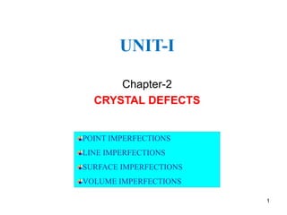
UIET KUK MED Time table Jan to May 2024.pdfupender3
The document contains a timetable for the Mechanical Engineering Department of UIET. It lists the time slots and lecture numbers for different courses on various days of the week. It also lists the faculty members teaching different courses and time slots allocated for labs. The timetable is divided into sections for undergraduate courses on top and postgraduate/research courses at the bottom. It provides a comprehensive overview of class and lab schedules for all courses in the department.
The document outlines a course on Condition Monitoring. The course aims to teach students how to understand vibration causes and faults, and apply monitoring techniques like oil analysis, vibration monitoring, and other diagnostic methods to identify issues and develop effective maintenance schemes for industries. Students will learn oil analysis to diagnose wear debris, nonconventional diagnostic methods, modern maintenance technologies, and apply vibration monitoring to identify system issues over 3 lecture hours for 3 credits, assessed through major and minor tests.
Inspection using Liquid penetrant testing.pptxupender3
This document outlines standards and procedures for inspecting DPT including acceptable standards, personal qualifications, indications for inspection, evaluations of indications, acceptance criteria, and repair criteria. Key areas covered are the qualifications of inspectors, what should trigger an inspection, how inspections should be evaluated, and what criteria determine if repairs are needed.
A creep test subjects a specimen to a constant load and temperature over time to measure deformation. There are three creep stages: primary creep where the rate is rapid and decreases over time, secondary creep where the rate is relatively uniform, and tertiary creep where the rate accelerates until rupture. Creep tests are used to determine design parameters like steady-state creep rate and rupture lifetime. Stress rupture tests are similar but impose higher stresses to measure time to fracture. Data from creep tests are used to extrapolate lifetimes at different conditions using methods like the Larson-Miller parameter.
Phase diagrams provide information about the equilibrium conditions and transformations between different phases in a material system. They describe how the phases of a material vary with changes in temperature, pressure, and composition.
This document discusses key concepts related to phase diagrams including phases, the Gibbs phase rule, one-component and binary phase diagrams, eutectic and peritectic reactions, intermediate phases, ternary diagrams, and lever rule. It provides examples of phase diagrams for common material systems like water, Cu-Ni, Pb-Sn, Mg-Pb, and Cu-Zn. Cooling curves are also explained to illustrate phase transformations.
Fatigue refers to damage accumulated through repeated cyclic stresses over time. It is affected by factors like stress type/amplitude, surface finish, material properties, and environment. Fatigue life depends on the mean and amplitude of stresses based on relationships like the Goodman diagram. The Miner's rule states that the fraction of fatigue life consumed by stresses must be less than 1 to avoid failure. Fatigue tests involve repeated cyclic loading in tension, compression, bending, or other patterns to determine fatigue properties.
Creep is a time-dependent deformation of materials that occurs when they are subjected to high temperatures and/or constant stress over long periods of time. It involves the gradual deformation of materials as atoms slowly migrate and rearrange. Creep can lead to sudden fracture or impaired usefulness of structural components. The creep strength of a material represents the highest stress it can withstand over time without exceeding a specified creep strain. Creep behavior is determined through tests that apply different stress levels to specimens at constant temperature and measure the time to failure. Fatigue is the failure of materials caused by repetitive cyclic stresses, even if the stresses are below the yield strength. It can be quantified using an S-N curve, which plots the stress amplitude against the number
The document discusses time-temperature-transformation (TTT) diagrams, which show the microstructural phases that form in steels at different temperatures over time. In contrast to equilibrium phase diagrams, TTT diagrams account for nonequilibrium cooling rates. They indicate that at higher temperatures, pearlite forms with slow cooling, while faster cooling produces bainite or martensite. The document includes an example TTT diagram for eutectoid steel and explains how isothermal experiments at different temperatures are used to construct these diagrams.
1) Proper design of the gating system is important for solidification and depends on factors like mold geometry, metal flow, and heat transfer.
2) The gating system includes components like the sprue, runner, and ingate and is designed based on principles of fluid flow like Bernoulli's theorem and the law of continuity.
3) Risers are used to prevent shrinkage voids and their design must ensure the riser remains molten until solidification is complete to feed the casting. The size and placement of risers depends on properties of the casting like its shape and surface area to volume ratio.
AE-681 Composite Materials is a 4 credit course taught by Dr. PM Mohite. The course covers topics such as introduction to unidirectional composites, analysis of lamina using classical laminate theory, design considerations, micromechanics, and performance under adverse environments. Reference materials include textbooks on composite materials and research papers. The grading policy includes assignments, midterm exams, and a final exam. Attendance will be monitored and late or copied assignments will be penalized.
Polymers are large molecules composed of repeating subunits called monomers. They can be natural or synthetic. Common synthetic polymers include plastics, nylon, and latex. Polymers are used in many applications because they are lightweight, strong, and inexpensive. They consist of long chains of monomers that can interact through entanglement and cross-linking to form durable materials.
Ultrasonic testing uses high frequency sound waves to detect surface and subsurface defects. It can be used to inspect thick sections non-destructively. There are different modes of wave propagation including longitudinal, transverse, surface waves and Lamb waves. Factors like frequency, penetration depth and scattering affect ultrasonic testing. It is widely used in manufacturing and service industries to inspect welds and structural metals.
The document provides information on heat treatment processes and the fundamentals of heat treatment of metals. It discusses the Fe-C equilibrium diagram and various phases in steel like ferrite, cementite, austenite, and pearlite. It describes the microstructure and properties of these phases. It also covers heat treatment processes like annealing, normalizing, hardening and discusses methods of surface hardening, heat treatment of cast irons and nonferrous metals. Various heat treatment parameters and objectives are defined. Diagrams of phase transformations and microstructures are included.
Point defects, such as vacancies and interstitials, are zero-dimensional imperfections in crystals. Line defects called dislocations are one-dimensional imperfections caused by a disruption of the stacking of atomic planes along a line. Dislocations can be edge or screw types. Surface imperfections are two-dimensional and include grain boundaries between crystals of different orientations, as well as twin boundaries and stacking faults. Volume imperfections are three-dimensional and include cracks, voids, and non-crystalline regions in a crystal. The presence of defects increases the potential energy of crystals.
A SYSTEMATIC RISK ASSESSMENT APPROACH FOR SECURING THE SMART IRRIGATION SYSTEMSIJNSA Journal
The smart irrigation system represents an innovative approach to optimize water usage in agricultural and landscaping practices. The integration of cutting-edge technologies, including sensors, actuators, and data analysis, empowers this system to provide accurate monitoring and control of irrigation processes by leveraging real-time environmental conditions. The main objective of a smart irrigation system is to optimize water efficiency, minimize expenses, and foster the adoption of sustainable water management methods. This paper conducts a systematic risk assessment by exploring the key components/assets and their functionalities in the smart irrigation system. The crucial role of sensors in gathering data on soil moisture, weather patterns, and plant well-being is emphasized in this system. These sensors enable intelligent decision-making in irrigation scheduling and water distribution, leading to enhanced water efficiency and sustainable water management practices. Actuators enable automated control of irrigation devices, ensuring precise and targeted water delivery to plants. Additionally, the paper addresses the potential threat and vulnerabilities associated with smart irrigation systems. It discusses limitations of the system, such as power constraints and computational capabilities, and calculates the potential security risks. The paper suggests possible risk treatment methods for effective secure system operation. In conclusion, the paper emphasizes the significant benefits of implementing smart irrigation systems, including improved water conservation, increased crop yield, and reduced environmental impact. Additionally, based on the security analysis conducted, the paper recommends the implementation of countermeasures and security approaches to address vulnerabilities and ensure the integrity and reliability of the system. By incorporating these measures, smart irrigation technology can revolutionize water management practices in agriculture, promoting sustainability, resource efficiency, and safeguarding against potential security threats.
Literature Review Basics and Understanding Reference Management.pptxDr Ramhari Poudyal
Three-day training on academic research focuses on analytical tools at United Technical College, supported by the University Grant Commission, Nepal. 24-26 May 2024
International Conference on NLP, Artificial Intelligence, Machine Learning an...gerogepatton
International Conference on NLP, Artificial Intelligence, Machine Learning and Applications (NLAIM 2024) offers a premier global platform for exchanging insights and findings in the theory, methodology, and applications of NLP, Artificial Intelligence, Machine Learning, and their applications. The conference seeks substantial contributions across all key domains of NLP, Artificial Intelligence, Machine Learning, and their practical applications, aiming to foster both theoretical advancements and real-world implementations. With a focus on facilitating collaboration between researchers and practitioners from academia and industry, the conference serves as a nexus for sharing the latest developments in the field.
DEEP LEARNING FOR SMART GRID INTRUSION DETECTION: A HYBRID CNN-LSTM-BASED MODELgerogepatton
As digital technology becomes more deeply embedded in power systems, protecting the communication
networks of Smart Grids (SG) has emerged as a critical concern. Distributed Network Protocol 3 (DNP3)
represents a multi-tiered application layer protocol extensively utilized in Supervisory Control and Data
Acquisition (SCADA)-based smart grids to facilitate real-time data gathering and control functionalities.
Robust Intrusion Detection Systems (IDS) are necessary for early threat detection and mitigation because
of the interconnection of these networks, which makes them vulnerable to a variety of cyberattacks. To
solve this issue, this paper develops a hybrid Deep Learning (DL) model specifically designed for intrusion
detection in smart grids. The proposed approach is a combination of the Convolutional Neural Network
(CNN) and the Long-Short-Term Memory algorithms (LSTM). We employed a recent intrusion detection
dataset (DNP3), which focuses on unauthorized commands and Denial of Service (DoS) cyberattacks, to
train and test our model. The results of our experiments show that our CNN-LSTM method is much better
at finding smart grid intrusions than other deep learning algorithms used for classification. In addition,
our proposed approach improves accuracy, precision, recall, and F1 score, achieving a high detection
accuracy rate of 99.50%.
CHINA’S GEO-ECONOMIC OUTREACH IN CENTRAL ASIAN COUNTRIES AND FUTURE PROSPECTjpsjournal1
The rivalry between prominent international actors for dominance over Central Asia's hydrocarbon
reserves and the ancient silk trade route, along with China's diplomatic endeavours in the area, has been
referred to as the "New Great Game." This research centres on the power struggle, considering
geopolitical, geostrategic, and geoeconomic variables. Topics including trade, political hegemony, oil
politics, and conventional and nontraditional security are all explored and explained by the researcher.
Using Mackinder's Heartland, Spykman Rimland, and Hegemonic Stability theories, examines China's role
in Central Asia. This study adheres to the empirical epistemological method and has taken care of
objectivity. This study analyze primary and secondary research documents critically to elaborate role of
china’s geo economic outreach in central Asian countries and its future prospect. China is thriving in trade,
pipeline politics, and winning states, according to this study, thanks to important instruments like the
Shanghai Cooperation Organisation and the Belt and Road Economic Initiative. According to this study,
China is seeing significant success in commerce, pipeline politics, and gaining influence on other
governments. This success may be attributed to the effective utilisation of key tools such as the Shanghai
Cooperation Organisation and the Belt and Road Economic Initiative.
Understanding Inductive Bias in Machine LearningSUTEJAS
This presentation explores the concept of inductive bias in machine learning. It explains how algorithms come with built-in assumptions and preferences that guide the learning process. You'll learn about the different types of inductive bias and how they can impact the performance and generalizability of machine learning models.
The presentation also covers the positive and negative aspects of inductive bias, along with strategies for mitigating potential drawbacks. We'll explore examples of how bias manifests in algorithms like neural networks and decision trees.
By understanding inductive bias, you can gain valuable insights into how machine learning models work and make informed decisions when building and deploying them.
Advanced control scheme of doubly fed induction generator for wind turbine us...IJECEIAES
This paper describes a speed control device for generating electrical energy on an electricity network based on the doubly fed induction generator (DFIG) used for wind power conversion systems. At first, a double-fed induction generator model was constructed. A control law is formulated to govern the flow of energy between the stator of a DFIG and the energy network using three types of controllers: proportional integral (PI), sliding mode controller (SMC) and second order sliding mode controller (SOSMC). Their different results in terms of power reference tracking, reaction to unexpected speed fluctuations, sensitivity to perturbations, and resilience against machine parameter alterations are compared. MATLAB/Simulink was used to conduct the simulations for the preceding study. Multiple simulations have shown very satisfying results, and the investigations demonstrate the efficacy and power-enhancing capabilities of the suggested control system.
ACEP Magazine edition 4th launched on 05.06.2024Rahul
This document provides information about the third edition of the magazine "Sthapatya" published by the Association of Civil Engineers (Practicing) Aurangabad. It includes messages from current and past presidents of ACEP, memories and photos from past ACEP events, information on life time achievement awards given by ACEP, and a technical article on concrete maintenance, repairs and strengthening. The document highlights activities of ACEP and provides a technical educational article for members.
Embedded machine learning-based road conditions and driving behavior monitoringIJECEIAES
Car accident rates have increased in recent years, resulting in losses in human lives, properties, and other financial costs. An embedded machine learning-based system is developed to address this critical issue. The system can monitor road conditions, detect driving patterns, and identify aggressive driving behaviors. The system is based on neural networks trained on a comprehensive dataset of driving events, driving styles, and road conditions. The system effectively detects potential risks and helps mitigate the frequency and impact of accidents. The primary goal is to ensure the safety of drivers and vehicles. Collecting data involved gathering information on three key road events: normal street and normal drive, speed bumps, circular yellow speed bumps, and three aggressive driving actions: sudden start, sudden stop, and sudden entry. The gathered data is processed and analyzed using a machine learning system designed for limited power and memory devices. The developed system resulted in 91.9% accuracy, 93.6% precision, and 92% recall. The achieved inference time on an Arduino Nano 33 BLE Sense with a 32-bit CPU running at 64 MHz is 34 ms and requires 2.6 kB peak RAM and 139.9 kB program flash memory, making it suitable for resource-constrained embedded systems.
A review on techniques and modelling methodologies used for checking electrom...nooriasukmaningtyas
The proper function of the integrated circuit (IC) in an inhibiting electromagnetic environment has always been a serious concern throughout the decades of revolution in the world of electronics, from disjunct devices to today’s integrated circuit technology, where billions of transistors are combined on a single chip. The automotive industry and smart vehicles in particular, are confronting design issues such as being prone to electromagnetic interference (EMI). Electronic control devices calculate incorrect outputs because of EMI and sensors give misleading values which can prove fatal in case of automotives. In this paper, the authors have non exhaustively tried to review research work concerned with the investigation of EMI in ICs and prediction of this EMI using various modelling methodologies and measurement setups.
2. 2
CRYSTAL DEFECTS AND IMPERFECTIONS
An ideal crystal is a perfect crystal in which each atom
has identical surroundings. Real crystals are not perfect.
A real crystal always has a large number of
imperfections in the lattice.
Since real crystals are of finite size, they have a surface
to their boundary.
At the boundary, atomic bonds terminate and hence the
surface itself is an imperfection.
One can reduce crystal defects considerably, but can
never eliminate them entirely.
4. 4
CRYSTAL DEFECTS AND IMPERFECTIONS
The study of imperfections has a two fold purpose, namely,
A better understanding of crystals and how they affect the
properties of metals.
Exploration of possibilities of minimizing or eliminating these
defects.
The term “defect” or “imperfection” is generally used to
describe any deviation from the perfect periodic array of
atoms in the crystal.
5. 5
CRYSTAL DEFECTS AND IMPERFECTIONS
Crystal imperfections can be classified on the basis of their
geometry as,
Point Imperfections,
Line imperfections
Surface (or) plane imperfections and
Volume imperfections
6. 6
POINT IMPERFECTIONS
They are imperfect point- like regions, one or two
atomic diameters in size and hence referred to as
‘zero dimensional imperfections’.
There are different kinds of point imperfections.
VACANCIES
If an atom is missing from its normal site in the
matrix, the defect is called a vacancy defect.
It may be a single vacancy, divacancy or a trivacancy.
8. 8
POINT IMPERFECTIONS
In metals vacancies and created by thermal excitation.
When the temperature is sufficiently high, as the atoms vibrate
around their regular positions, some acquire enough energy to leave
the site completely.
When the regular atom leaves, a vacancy is created.
A pair of one cation and one anion can be missed from an ionic
crystal.Such a pair of vacant ion sites is called Schottky imperfection.
This type of defect is dominant in alkali halides.
10. 10
SUBSTITUTIONAL IMPURITY
It refers to a foreign atom that substitutes for or
replaces a parent atom in the crystal.
Pentavalent or trivalent impurity atoms doped
in Silicon or Germanium are also substitutional
impurities in the crystal.
12. 12
INTERSTITIAL IMPURITY
An interstitial defect arises when an atom occupies a
definite position in the lattice that is not normally occupied
in the perfect crystal.
In crystals, packing density is always less than 1.
If a small sized atom occupies the void space in the parent
crystal without disturbing the parent atoms from their
regular sites, then it is called as ‘interstitial impurity’.
14. 14
INTERSTITIAL IMPURITY
In ionic crystals, an ion displaced from a regular site to an
interstitial site is called ‘Frenkel imperfection’.
As cations are generally the smaller ones, it is possible for
them to get displaced into the void space.
Anions do not get displaced as the void space is too small
compared to the size of the anions.
A Frenkel imperfection does not change the overall electrical
neutrality of the crystal. This type of defect occurs in silver
halides and CaF2.
16. 16
ELECTRONIC DEFECTS
Errors in charge distribution in solids are called
‘electronic defects’.
These defects are produced when the composition of
an ionic crystal does not correspond to the exact
stoichiometric formula.
These defects are free to move in the crystal under
the influence of an electric field.
17. 17
EFFECT OF POINT IMPERFECTIONS
The presence of a point imperfection introduces distortions in
the crystal.
In the case of impurity atom, because of its difference in size,
elastic strains are created in the regions surrounding the
impurity atom.
All these factors tend to increase the potential energy of the
crystal called ‘enthalpy’.
The work done for the creation of such a point defect is called
the ‘enthalpy of formation’ of the point imperfection.
18. 18
LINE IMPERFECTIONS
The defects, which take place due to dislocation or
distortion of atoms along a line, in some direction are
called as ‘line defects’.
Line defects are also called dislocations. In the geometic
sense, they may be called as ‘one dimensional defects’.
A dislocation may be defined as a disturbed region
between two substantially perfect parts of a crystal.
It is responsible for the phenomenon of slip by which
most metals deform plastically.
21. 21
EDGE DISLOCATION
In perfect crystal, atoms are arranged in both vertical and
horizontal planes parallel to the side faces.
If one of these vertical planes does not extend to the full
length, but ends in between within the crystal it is called ‘edge
dislocation’.
In the perfect crystal, just above the edge of the incomplete
plane the atoms are squeezed and are in a state of compression.
Just below the edge of the incomplete plane, the atoms are
pulled apart and are in a state of tension.
22. 22
The distorted configuration extends all along the edge into the
crystal.
Thus as the region of maximum distortion is centered around
the edge of the incomplete plane, this distortion represents a line
imperfection and is called an edge dislocation.
Edge dislocations are represented by ‘’ or ‘‘ depending on
whether the incomplete plane starts from the top or from the
bottom of the crystal.
These two configurations are referred to as positive and
negative edge dislocations respectively.
EDGE DISLOCATION
27. 27
BURGERS VECTOR
The magnitude and the
direction of the displacement are
defined by a vector, called the
Burgers Vector.
In figure (a), starting from the
point P, we go up by 6 steps, then
move towards right by 5 steps,
move down by 6 steps and finally
move towards left by 5 steps to
reach the starting point P.Now the
Burgers circuit gets closed.
When the same operation is
performed on the defect crystal
(figure (b)) we end up at Q
instead of the starting point.
29. 29
BURGERS VECTOR
So, we have to move an extra step to return to P, in order to close
the Burgers circuit.
The magnitude and the direction of the step defines the Burgers
Vector (BV).
The Burgers Vector is perpendicular to the edge dislocation line.
30. 30
SCREW DISLOCATION
In this dislocation, the
atoms are displaced in two
separate planes
perpendicular to each other.
It forms a spiral ramp
around the dislocation.
The Burgers Vector is
parallel to the screw
dislocation line.
Speed of movement of a
screw dislocation is lesser
compared to edge
dislocation. Normally, the
real dislocations in the
crystals are the mixtures of
edge and screw dislocation.
58. • The stress required to cause the dislocation to move increases exponentially with
the length of the Burgers vector. Thus, the slip direction should have a small
repeat distance or high linear density. The close-packed directions in metals and
alloys satisfy this criterion and are the usual slip directions.
• The stress required to cause the dislocation to move decreases exponentially with
the interplanar spacing of the slip planes. Slip occurs most easily between planes
of atoms that are smooth (so there are smaller ‘‘hills and valleys’’ on the surface)
and between planes that are far apart (or have a relatively large interplanar
spacing). Planes with a high planar density fulfill this requirement. Therefore the
slip planes are typically close-packed planes or those as closely packed as possible.
• Dislocations do not move easily in materials such as silicon or polymers, which
have covalent bonds. Because of the strength and directionality of the bonds, the
materials typically fail in a brittle manner before the force becomes high enough
to cause appreciable slip. In many engineering polymers dislocations play a
relatively minor role in their deformation.
• Materials with ionic bonding, including many ceramics such as MgO, also are
resistant to slip. Movement of a dislocation disrupts the charge balance around
the anions and cations, requiring that bonds between anions and cations be
broken. During slip, ions with a like charge must also pass close together, causing
repulsion. Finally, the repeat distance along the slip direction, or the Burgers
vector, is larger than that in metals and alloys. 58
59. 59
SURFACE IMPERFECTIONS
Surface imperfections arise from a change in the stacking
of atomic planes on or across a boundary.
The change may be one of the orientations or of the
stacking sequence of atomic planes.
In geometric concept, surface imperfections are two-
dimensional. They are of two types external and internal
surface imperfections.
60. 60
EXTERNAL SURFACE IMPERFECTIONS
They are the imperfections represented by a boundary. At the
boundary the atomic bonds are terminated.
The atoms on the surface cannot be compared with the atoms
within the crystal. The reason is that the surface atoms have
neighbours on one side only. Where as the atoms inside the crystal
have neighbours on either sides. This is shown in figure in next
slide. Since these surface atoms are not surrounded by others,
they possess higher energy than that of internal atoms.
For most metals, the energy of the surface atoms is of the order
of 1 J/m2.
62. 62
INTERNAL SURFACE IMPERFECTIONS
Internal surface imperfections are the imperfections which
occurred inside a crystal.
It is caused by the defects such as, grain boundaries. tilt
boundaries, twin boundaries and stacking faults.
63. 63
GRAIN BOUNDARIES
They are the imperfections which separate crystals or grains of
different orientation in a poly crystalline solid during nucleation or
crystallization.
It is a two dimensional imperfection. During crystallization, new
crystals form in different parts and they are randomly oriented with
respect to one another.
They grow and impinge on each other.
The atoms held in between are attracted by crystals on either side
and depending on the forces, the atoms occupy equilibrium
positions.
64. 64
GRAIN BOUNDARIES
These positions at the boundary region between two crystals
are distorted.As a result, a region of transition exists in which
the atomic packing is imperfect.
The thickness of this region is 2 to 10 or more atomic
diameters.
The boundary region is called a crystal boundary or a grain
boundary .
The boundary between two crystals which have different
crystalline arrangements or different compositions, is called as
interphase boundary or commonly an interface.
66. 66
TILT BOUNDARIES
This is called low-angle boundary as the orientation
difference between two neighbouring crystals is less than 10°.
The disruption in the boundary is not so severe as in the
high-angle boundary. In general low-angle boundaries can be
described by suitable arrays of dislocation.
Actually a low-angle tilt boundary is composed of edge
dislocation lying one above the other
The angle or tilt will be
where b = Burgers vector and
D = the average vertical distance between dislocations.
D
b
68. 68
TWIN BOUNDARIES
If the atomic arrangement on one side of a boundary is a
mirror reflection of the arrangement on the other side, then it is
called as twin boundary.
As they occur in pair, they are called twin boundaries. At one
boundary, orientation of atomic arrangement changes.
At another boundary, it is restored back. The region between
the pair of boundaries is called the twinned region.
These boundaries are easily identified under an optical
microscope.
70. 70
STACKING FAULTS
Whenever the stacking of atomic planes is not in a proper
sequence throughout the crystal, the fault caused is known as
stacking fault.
For example, the stacking sequence in an ideal FCC crystal
may be described as A-B-C-A-B-C- A-B-C-……. But the
stacking fault may change the sequence to A-B-C-A-B-A-B-A-
B-C. The region in which the stacking fault occurs (A-B-A-B)
forms a thin region and it becomes HCP.
This thin region is a surface imperfection and is called a
stacking fault.
79. 79
A twin boundary is a reversal in the crystal lattice, such as ABC | BA-CBA-CBA.
(The | represents the point of the twin boundary, where the stacking order
reverses).
80. 80
In an antiphase region, a portion of material shifts over. For example: ABC-A|ABC-
ABC-ABC|C-ABC. The bolded portion has shifted over by one spot, which creates
antiphase boundaries so that two of the same layers are stacked on top of each
other.
84. 84
VOLUME IMPERFECTIONS
Volume defects such as cracks may arise in crystals when
there is only small electrostatic dissimilarity between the
stacking sequences of close packed planes in metals. Presence
of a large vacancy or void space, when cluster of atoms are
missed is also considered as a volume imperfection.
Foreign particle inclusions and non crystalline regions which
have the dimensions of the order of 0.20 nm are also called as
volume imperfections.