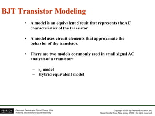
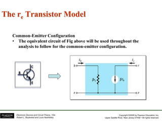
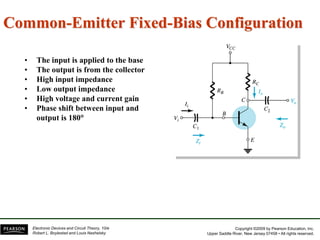
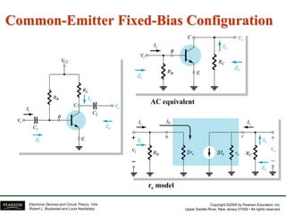
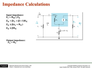
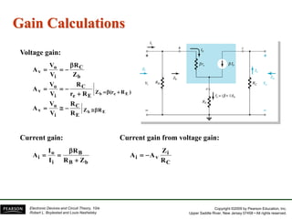
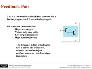
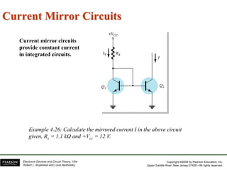
Chapter 5:
BJT AC Analysis
Copyright ©2009 by Pearson Education, Inc.
Upper Saddle River, New Jersey 07458 • All rights reserved.
Electronic Devices and Circuit Theory, 10/e
Robert L. Boylestad and Louis Nashelsky
BJT Transistor Modeling
• A model is an equivalent circuit that represents the AC
characteristics of the transistor.
• A model uses circuit elements that approximate the
behavior of the transistor.
• There are two models commonly used in small signal AC
analysis of a transistor:
– re model
– Hybrid equivalent model
Copyright ©2009 by Pearson Education, Inc.
Upper Saddle River, New Jersey 07458 • All rights reserved.
Electronic Devices and Circuit Theory, 10/e
Robert L. Boylestad and Louis Nashelsky
The re Transistor Model
• BJTs are basically current-controlled devices; therefore the re model
uses a diode and a current source to duplicate the behavior of the
transistor.
• One disadvantage to this model is its sensitivity to the DC level. This
model is designed for specific circuit conditions.
Copyright ©2009 by Pearson Education, Inc.
Upper Saddle River, New Jersey 07458 • All rights reserved.
Electronic Devices and Circuit Theory, 10/e
Robert L. Boylestad and Louis Nashelsky
The re Transistor Model
Common-Emitter Configuration
• The equivalent circuit of Fig above will be used throughout the
analysis to follow for the common-emitter configuration.
Copyright ©2009 by Pearson Education, Inc.
Upper Saddle River, New Jersey 07458 • All rights reserved.
Electronic Devices and Circuit Theory, 10/e
Robert L. Boylestad and Louis Nashelsky
Common-Emitter Fixed-Bias Configuration
• The input is applied to the base
• The output is from the collector
• High input impedance
• Low output impedance
• High voltage and current gain
• Phase shift between input and
output is 180
Copyright ©2009 by Pearson Education, Inc.
Upper Saddle River, New Jersey 07458 • All rights reserved.
Electronic Devices and Circuit Theory, 10/e
Robert L. Boylestad and Louis Nashelsky
Common-Emitter Fixed-Bias Configuration
AC equivalent
re model
Copyright ©2009 by Pearson Education, Inc.
Upper Saddle River, New Jersey 07458 • All rights reserved.
Electronic Devices and Circuit Theory, 10/e
Robert L. Boylestad and Louis Nashelsky
Common-Emitter Fixed-Bias Calculations
C
o 10R
r
e
C
v
e
o
C
i
o
v
r
R
A
r
)
r
||
(R
V
V
A






e
B
C
o r
10
R
,
10R
r
i
e
B
C
o
o
B
i
o
i
A
)
r
)(R
R
(r
r
R
I
I
A











C
i
v
i
R
Z
A
A 

Current gain from voltage gain:
Input impedance:
Output impedance:
Voltage gain: Current gain:
e
E r
10
R
e
i
e
B
i
r
Z
r
||
R
Z






C
o
O
R
10
r
C
o
C
o
R
Z
r
||
R
Z



Copyright ©2009 by Pearson Education, Inc.
Upper Saddle River, New Jersey 07458 • All rights reserved.
Electronic Devices and Circuit Theory, 10/e
Robert L. Boylestad and Louis Nashelsky
Common-Emitter Voltage-Divider Bias
re model requires you to determine , re, and ro.
Copyright ©2009 by Pearson Education, Inc.
Upper Saddle River, New Jersey 07458 • All rights reserved.
Electronic Devices and Circuit Theory, 10/e
Robert L. Boylestad and Louis Nashelsky
Common-Emitter Voltage-Divider Bias Cal.
Current gain from voltage gain:
Input impedance:
Output impedance:
Voltage gain:
Current gain:
e
i
2
1
r
||
R
Z
R
||
R
R





C
o 10R
r
C
o
o
C
o
R
Z
r
||
R
Z



C
o 10R
r
e
C
i
o
v
e
o
C
i
o
v
r
R
V
V
A
r
r
||
R
V
V
A







e
C
o
C
o
r
10
R
,
10R
r
i
o
i
10R
r
e
i
o
i
e
C
o
o
i
o
i
I
I
A
r
R
R
I
I
A
)
r
R
)(
R
(r
r
R
I
I
A























C
i
v
i
R
Z
A
A 

Copyright ©2009 by Pearson Education, Inc.
Upper Saddle River, New Jersey 07458 • All rights reserved.
Electronic Devices and Circuit Theory, 10/e
Robert L. Boylestad and Louis Nashelsky
Common-Emitter Emitter-Bias Config.
Copyright ©2009 by Pearson Education, Inc.
Upper Saddle River, New Jersey 07458 • All rights reserved.
Electronic Devices and Circuit Theory, 10/e
Robert L. Boylestad and Louis Nashelsky
Impedance Calculations
E
b
E
e
b
E
e
b
b
B
i
R
Z
)
R
(r
Z
1)R
(
r
Z
Z
||
R
Z











Input impedance:
Output impedance:
C
o R
Z 
Copyright ©2009 by Pearson Education, Inc.
Upper Saddle River, New Jersey 07458 • All rights reserved.
Electronic Devices and Circuit Theory, 10/e
Robert L. Boylestad and Louis Nashelsky
Gain Calculations
Current gain from voltage gain:
Voltage gain:
Current gain:
E
b
E
e
b
R
Z
E
C
i
o
v
)
R
(r
Z
E
e
C
i
o
v
b
C
i
o
v
R
R
V
V
A
R
r
R
V
V
A
Z
R
V
V
A
















b
B
B
i
o
i
Z
R
R
I
I
A




C
i
v
i
R
Z
A
A 

Copyright ©2009 by Pearson Education, Inc.
Upper Saddle River, New Jersey 07458 • All rights reserved.
Electronic Devices and Circuit Theory, 10/e
Robert L. Boylestad and Louis Nashelsky
Feedback Pair
This is a two-transistor circuit that operates like a
Darlington pair, but it is not a Darlington pair.
It has similar characteristics:
• High current gain
• Voltage gain near unity
• Low output impedance
• High input impedance
The difference is that a Darlington
uses a pair of like transistors,
whereas the feedback-pair
configuration uses complementary
transistors.
Copyright ©2009 by Pearson Education, Inc.
Upper Saddle River, New Jersey 07458 • All rights reserved.
Electronic Devices and Circuit Theory, 10/e
Robert L. Boylestad and Louis Nashelsky
Current Mirror Circuits
Current mirror circuits
provide constant current
in integrated circuits.
Example 4.26: Calculate the mirrored current I in the above circuit
given, Rx = 1.1 kΩ and +Vcc = 12 V.

Bem (8)

  • 1.
  • 2.
    Copyright ©2009 byPearson Education, Inc. Upper Saddle River, New Jersey 07458 • All rights reserved. Electronic Devices and Circuit Theory, 10/e Robert L. Boylestad and Louis Nashelsky BJT Transistor Modeling • A model is an equivalent circuit that represents the AC characteristics of the transistor. • A model uses circuit elements that approximate the behavior of the transistor. • There are two models commonly used in small signal AC analysis of a transistor: – re model – Hybrid equivalent model
  • 3.
    Copyright ©2009 byPearson Education, Inc. Upper Saddle River, New Jersey 07458 • All rights reserved. Electronic Devices and Circuit Theory, 10/e Robert L. Boylestad and Louis Nashelsky The re Transistor Model • BJTs are basically current-controlled devices; therefore the re model uses a diode and a current source to duplicate the behavior of the transistor. • One disadvantage to this model is its sensitivity to the DC level. This model is designed for specific circuit conditions.
  • 4.
    Copyright ©2009 byPearson Education, Inc. Upper Saddle River, New Jersey 07458 • All rights reserved. Electronic Devices and Circuit Theory, 10/e Robert L. Boylestad and Louis Nashelsky The re Transistor Model Common-Emitter Configuration • The equivalent circuit of Fig above will be used throughout the analysis to follow for the common-emitter configuration.
  • 5.
    Copyright ©2009 byPearson Education, Inc. Upper Saddle River, New Jersey 07458 • All rights reserved. Electronic Devices and Circuit Theory, 10/e Robert L. Boylestad and Louis Nashelsky Common-Emitter Fixed-Bias Configuration • The input is applied to the base • The output is from the collector • High input impedance • Low output impedance • High voltage and current gain • Phase shift between input and output is 180
  • 6.
    Copyright ©2009 byPearson Education, Inc. Upper Saddle River, New Jersey 07458 • All rights reserved. Electronic Devices and Circuit Theory, 10/e Robert L. Boylestad and Louis Nashelsky Common-Emitter Fixed-Bias Configuration AC equivalent re model
  • 7.
    Copyright ©2009 byPearson Education, Inc. Upper Saddle River, New Jersey 07458 • All rights reserved. Electronic Devices and Circuit Theory, 10/e Robert L. Boylestad and Louis Nashelsky Common-Emitter Fixed-Bias Calculations C o 10R r e C v e o C i o v r R A r ) r || (R V V A       e B C o r 10 R , 10R r i e B C o o B i o i A ) r )(R R (r r R I I A            C i v i R Z A A   Current gain from voltage gain: Input impedance: Output impedance: Voltage gain: Current gain: e E r 10 R e i e B i r Z r || R Z       C o O R 10 r C o C o R Z r || R Z   
  • 8.
    Copyright ©2009 byPearson Education, Inc. Upper Saddle River, New Jersey 07458 • All rights reserved. Electronic Devices and Circuit Theory, 10/e Robert L. Boylestad and Louis Nashelsky Common-Emitter Voltage-Divider Bias re model requires you to determine , re, and ro.
  • 9.
    Copyright ©2009 byPearson Education, Inc. Upper Saddle River, New Jersey 07458 • All rights reserved. Electronic Devices and Circuit Theory, 10/e Robert L. Boylestad and Louis Nashelsky Common-Emitter Voltage-Divider Bias Cal. Current gain from voltage gain: Input impedance: Output impedance: Voltage gain: Current gain: e i 2 1 r || R Z R || R R      C o 10R r C o o C o R Z r || R Z    C o 10R r e C i o v e o C i o v r R V V A r r || R V V A        e C o C o r 10 R , 10R r i o i 10R r e i o i e C o o i o i I I A r R R I I A ) r R )( R (r r R I I A                        C i v i R Z A A  
  • 10.
    Copyright ©2009 byPearson Education, Inc. Upper Saddle River, New Jersey 07458 • All rights reserved. Electronic Devices and Circuit Theory, 10/e Robert L. Boylestad and Louis Nashelsky Common-Emitter Emitter-Bias Config.
  • 11.
    Copyright ©2009 byPearson Education, Inc. Upper Saddle River, New Jersey 07458 • All rights reserved. Electronic Devices and Circuit Theory, 10/e Robert L. Boylestad and Louis Nashelsky Impedance Calculations E b E e b E e b b B i R Z ) R (r Z 1)R ( r Z Z || R Z            Input impedance: Output impedance: C o R Z 
  • 12.
    Copyright ©2009 byPearson Education, Inc. Upper Saddle River, New Jersey 07458 • All rights reserved. Electronic Devices and Circuit Theory, 10/e Robert L. Boylestad and Louis Nashelsky Gain Calculations Current gain from voltage gain: Voltage gain: Current gain: E b E e b R Z E C i o v ) R (r Z E e C i o v b C i o v R R V V A R r R V V A Z R V V A                 b B B i o i Z R R I I A     C i v i R Z A A  
  • 13.
    Copyright ©2009 byPearson Education, Inc. Upper Saddle River, New Jersey 07458 • All rights reserved. Electronic Devices and Circuit Theory, 10/e Robert L. Boylestad and Louis Nashelsky Feedback Pair This is a two-transistor circuit that operates like a Darlington pair, but it is not a Darlington pair. It has similar characteristics: • High current gain • Voltage gain near unity • Low output impedance • High input impedance The difference is that a Darlington uses a pair of like transistors, whereas the feedback-pair configuration uses complementary transistors.
  • 14.
    Copyright ©2009 byPearson Education, Inc. Upper Saddle River, New Jersey 07458 • All rights reserved. Electronic Devices and Circuit Theory, 10/e Robert L. Boylestad and Louis Nashelsky Current Mirror Circuits Current mirror circuits provide constant current in integrated circuits. Example 4.26: Calculate the mirrored current I in the above circuit given, Rx = 1.1 kΩ and +Vcc = 12 V.