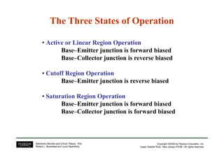
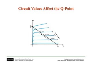
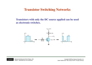
The document discusses various biasing circuits for BJT transistors including:
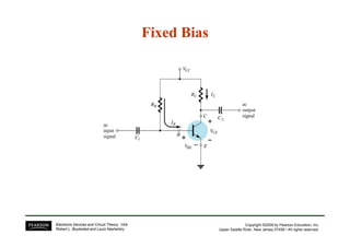
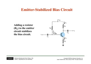
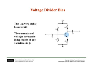
1) Fixed bias, emitter-stabilized bias, and voltage divider bias circuits which establish a quiescent operating point (Q-point) for the transistor.
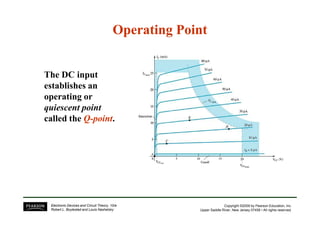
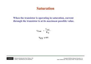
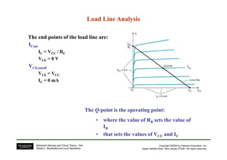
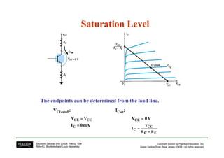
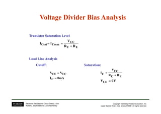
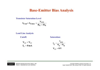
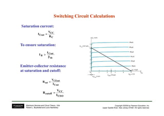
2) Load line analysis is used to determine the Q-point and saturation/cutoff points by considering the transistor's I-V characteristics and the external circuit.
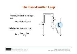
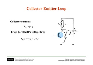
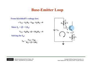
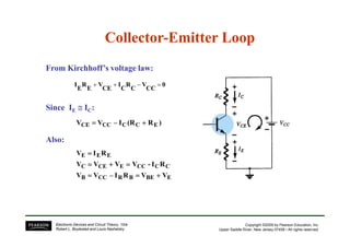
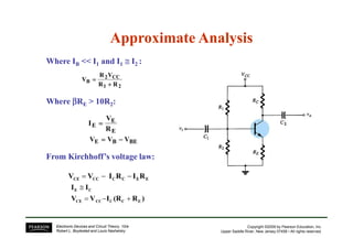
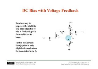
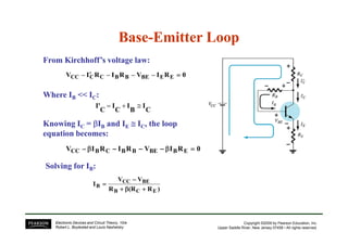
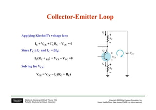
3) DC bias circuits can be analyzed by applying Kirchhoff's laws to the base-emitter and collector-emitter loops.


![[Deck] What's New in Spark-Iceberg Integration via DSV2.pptx](https://cdn.slidesharecdn.com/ss_thumbnails/deckwhatsnewinspark-icebergintegrationviadsv2-260210005337-25955b12-thumbnail.jpg?width=640&height=640&fit=bounds)


