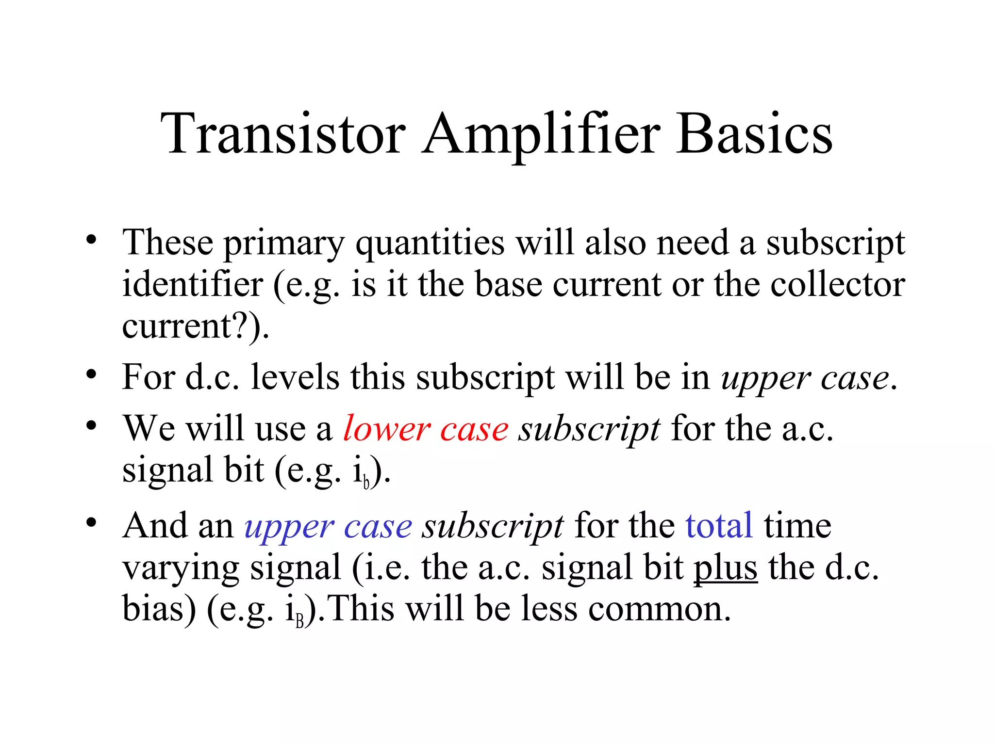
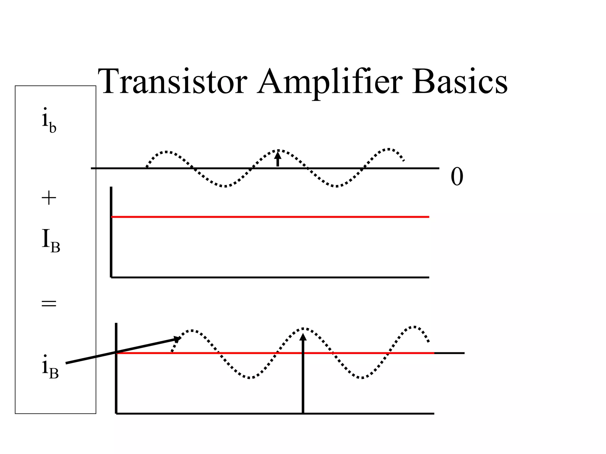
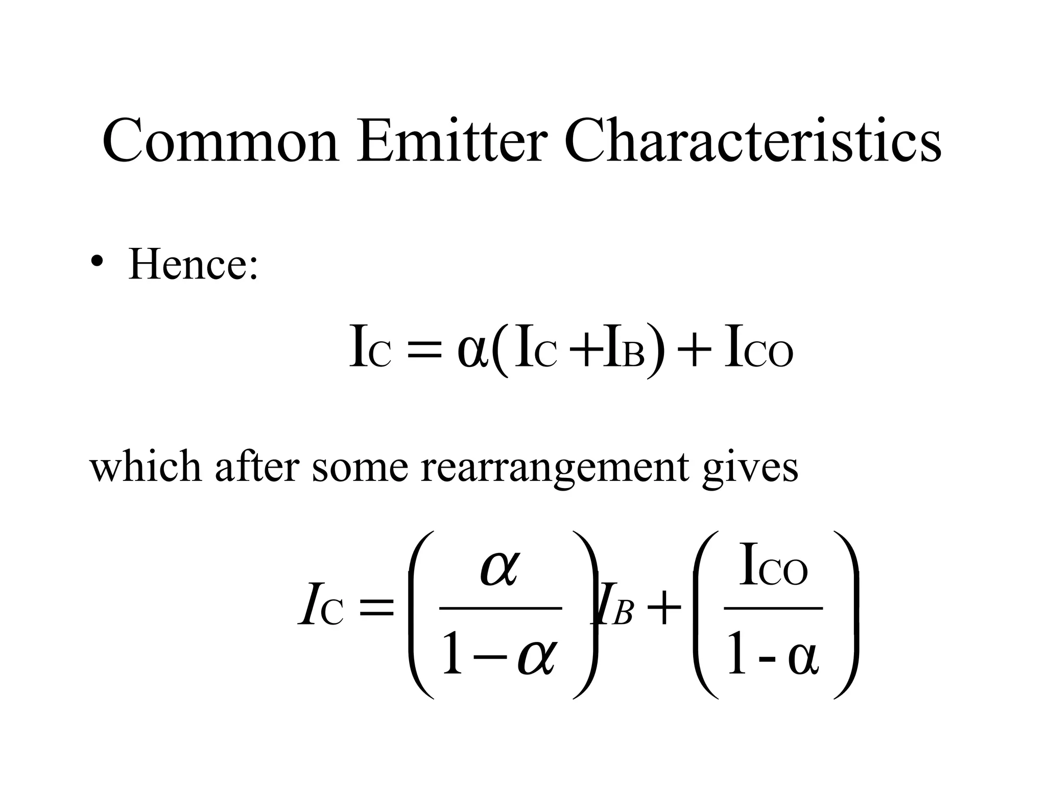
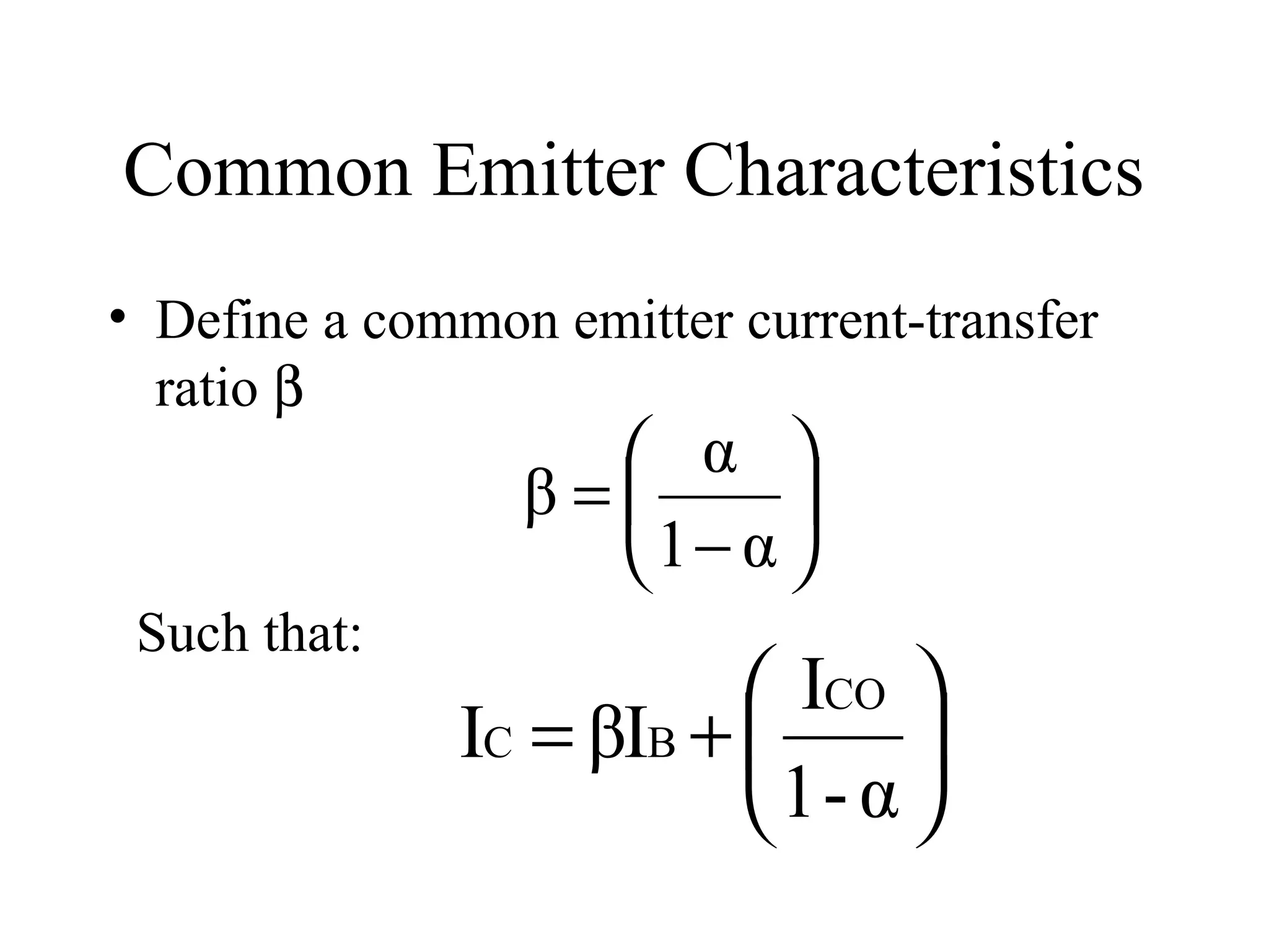
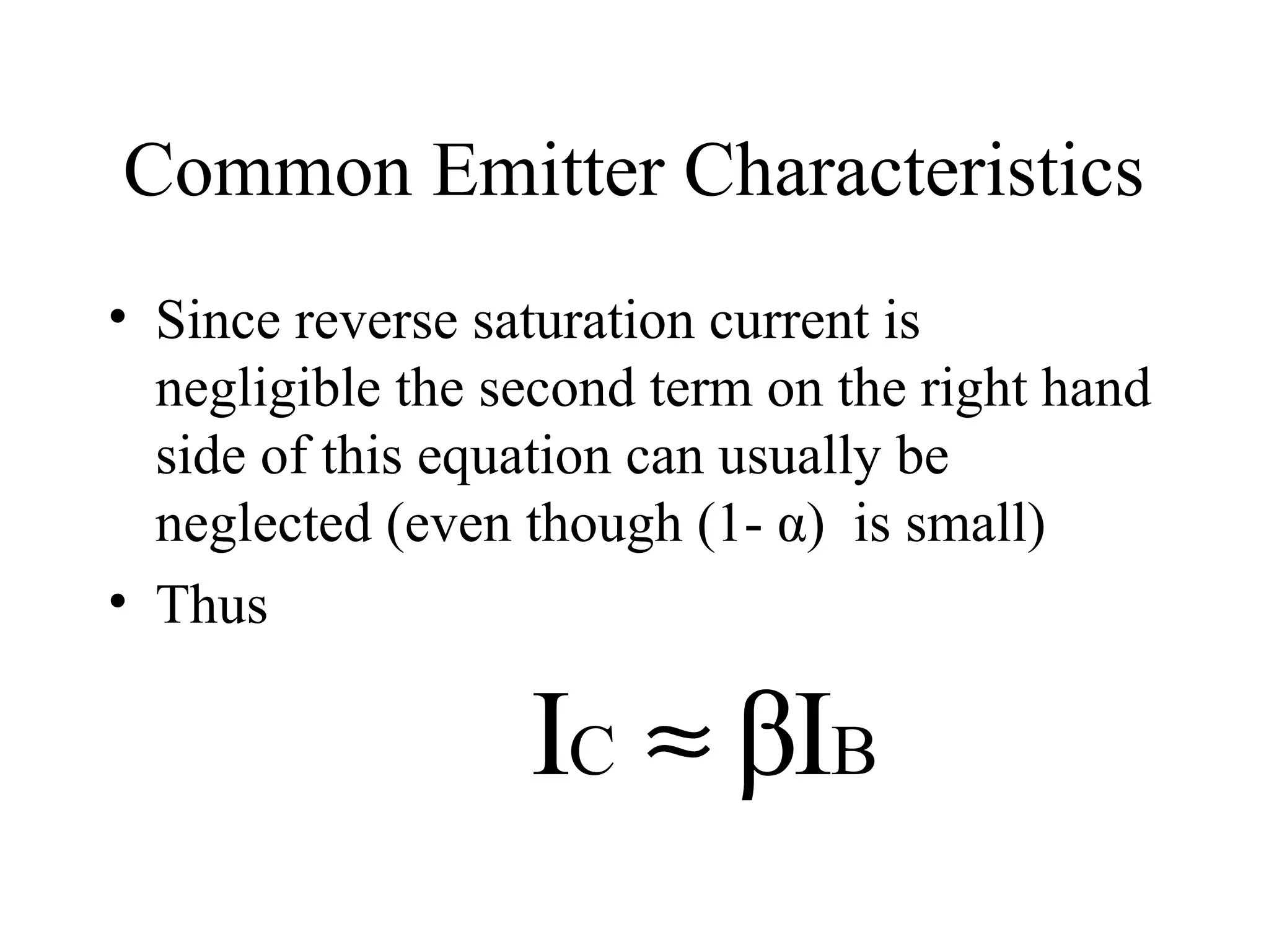
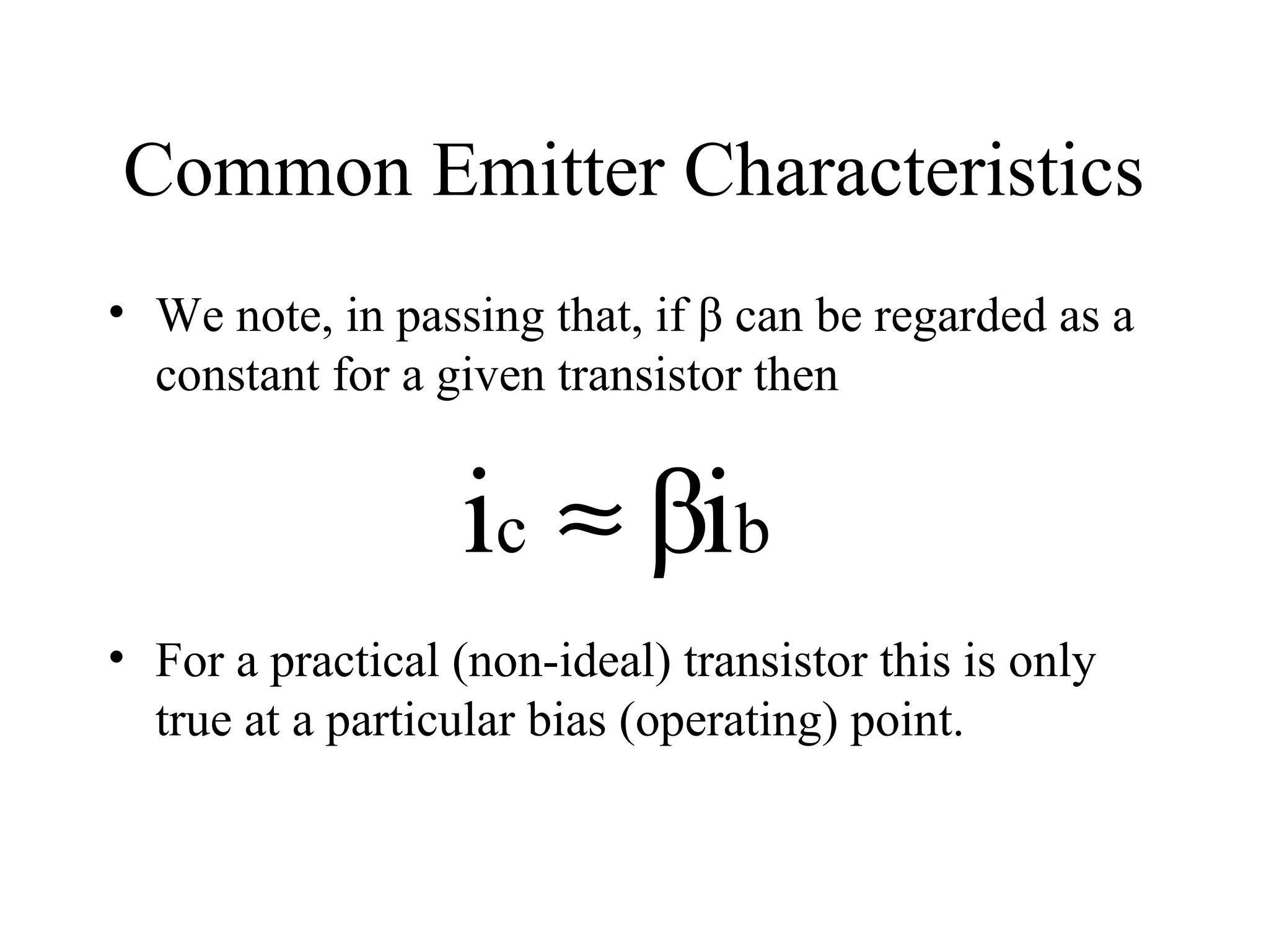
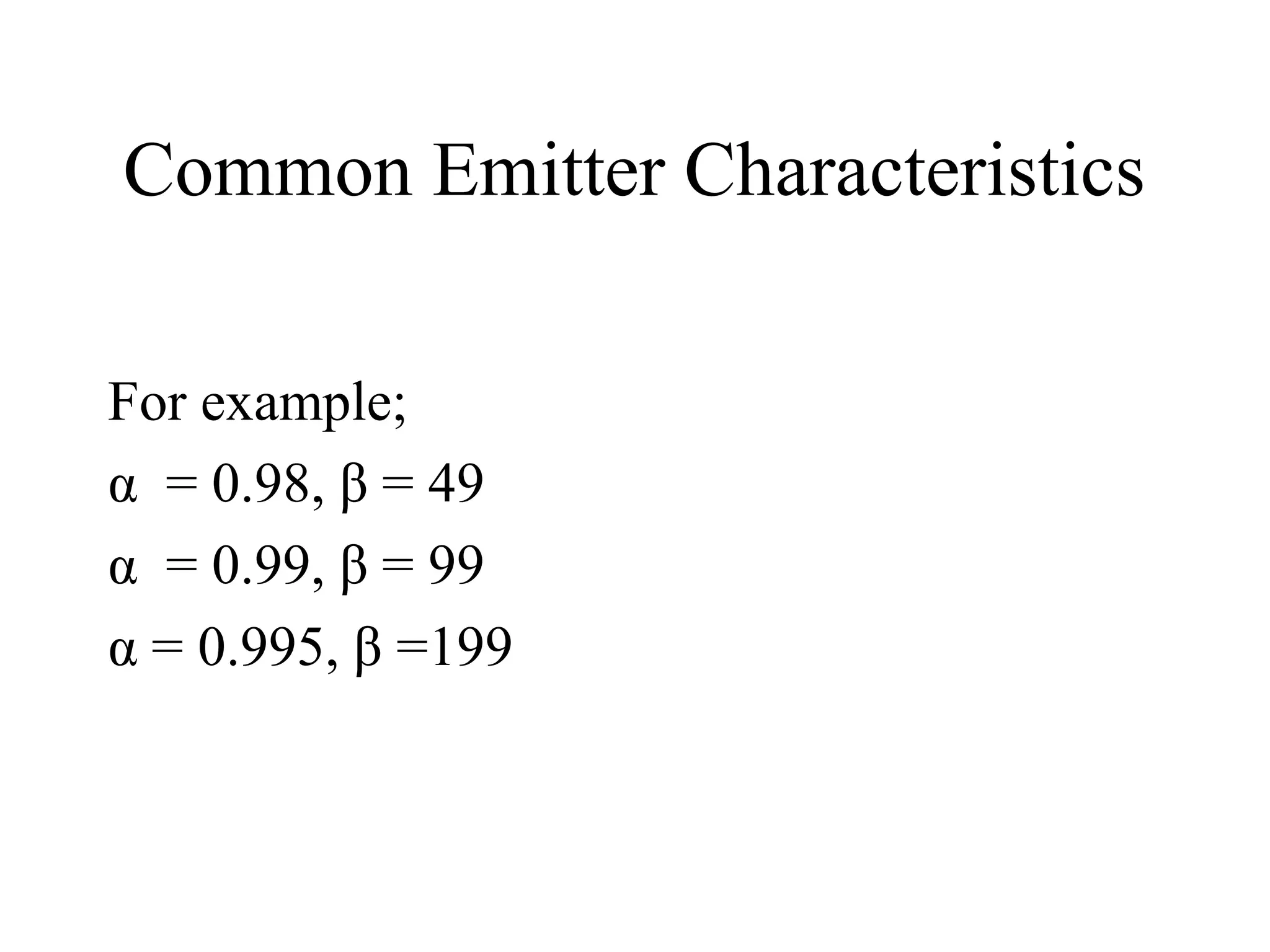
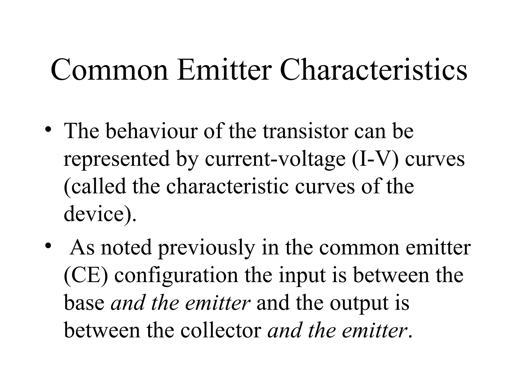
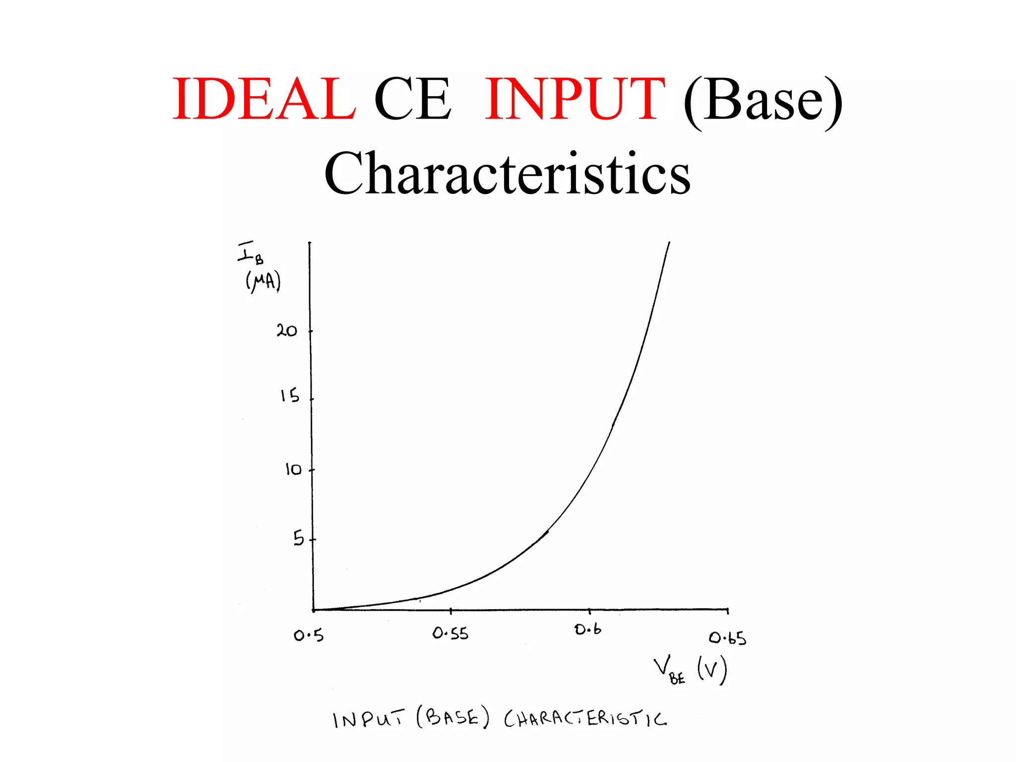
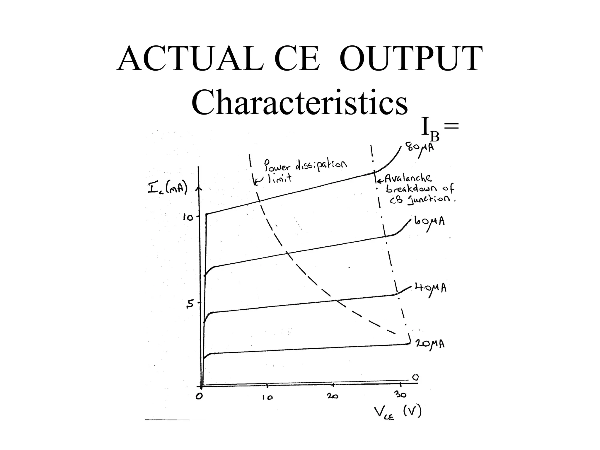
EXPERT SYSTEMS AND SOLUTIONS
     Email: expertsyssol@gmail.com
        expertsyssol@yahoo.com
          Cell: 9952749533
     www.researchprojects.info
    PAIYANOOR, OMR, CHENNAI
 Call For Research Projects          Final
 year students of B.E in EEE, ECE,
    EI, M.E (Power Systems), M.E
  (Applied Electronics), M.E (Power
              Electronics)
  Ph.D Electrical and Electronics.
Students can assemble their hardware in our
 Research labs. Experts will be guiding the
                 projects.
Transistor Amplifier Basics
• It is critical to understand the notation used
  for voltages and currents in the following
  discussion of transistor amplifiers.
• This is therefore dealt with explicitly ‘up
  front’.
• As with dynamic resistance in diodes we
  will be dealing with a.c. signals
  superimposed on d.c. bias levels.
Transistor Amplifier Basics
• We will use a capital (upper case) letter for
  a d.c. quantity (e.g. I, V).
• We will use a lower case letter for a time
  varying (a.c.) quantity (e.g. i, v)
Transistor Amplifier Basics
• These primary quantities will also need a subscript
  identifier (e.g. is it the base current or the collector
  current?).
• For d.c. levels this subscript will be in upper case.
• We will use a lower case subscript for the a.c.
  signal bit (e.g. ib).
• And an upper case subscript for the total time
  varying signal (i.e. the a.c. signal bit plus the d.c.
  bias) (e.g. iB).This will be less common.
Transistor Amplifier Basics
ib

                            0
+
IB

=

iB
Transistor Amplifier Basics
• It is convention to refer all transistor
  voltages to the ‘common’ terminal.
• Thus in the CE configuration we would
  write VCE for a d.c. collector emitter voltage
  and VBE for a d.c. base emitter voltage.
Common Emitter Characteristics
• For the present we consider DC behaviour
  and assume that we are working in the
  normal linear amplifier regime with the
  BE junction forward biased and the CB
  junction reverse biased
Common Emitter Characteristics
Treating the transistor as a current node:
               IE = IC +IB
• Also:

              IC =α IE + Ico
Common Emitter Characteristics
• Hence:
             IC = α( ΙC +IB) + ICO
which after some rearrangement gives

                 α        ICO 
           IC =     IB +       
                1−α       1- α 
Common Emitter Characteristics
• Define a common emitter current-transfer
  ratio β
                    α 
                 β=     
                   1− α 
 Such that:
                          ICO 
              IC = βIB +       
                          1- α 
Common Emitter Characteristics
• Since reverse saturation current is
  negligible the second term on the right hand
  side of this equation can usually be
  neglected (even though (1- α) is small)
• Thus

                  IC ≈ βIB
Common Emitter Characteristics
• We note, in passing that, if β can be regarded as a
  constant for a given transistor then


                  ic ≈ βib
• For a practical (non-ideal) transistor this is only
  true at a particular bias (operating) point.
Common Emitter Characteristics
• A small change in α causes a much bigger
  change in ß which means that ß can vary
  significantly, even from transistor to
  transistor of the same type.
• We must try and allow for these variations
  in circuit design.
Common Emitter Characteristics

For example;
α = 0.98, β = 49
α = 0.99, β = 99
α = 0.995, β =199
Common Emitter Characteristics

∀ β is also known as hFE and may appear on
  data sheets and in some textbooks as such.

• For a given transistor type data sheets may
  specify a range of β values
Common Emitter Characteristics
• The behaviour of the transistor can be
  represented by current-voltage (I-V) curves
  (called the characteristic curves of the
  device).
• As noted previously in the common emitter
  (CE) configuration the input is between the
  base and the emitter and the output is
  between the collector and the emitter.
Common Emitter Characteristics
• We can therefore draw an input
  characteristic (plotting base current IB
  against base-emitter voltage VBE) and
• an output characteristic (plotting collector
  current Ic against collector-emitter voltage
  VCE)
Common Emitter Characteristics
• We will be using these characteristic curves
  extensively to understand:
• How the transistor operates as a linear
  amplifier for a.c. signals.
• The need to superimpose the a.c. signals on
  d.c. bias levels.
• The relationship between the transistor and
  the circuit in which it is placed.
Common Emitter Characteristics
• Once these basics are understood we will
  understand:
• Why we can replace the transistor by a
  small signal (a.c.) equivalent circuit.
• How to derive a simple a.c. equivalent
  circuit from the characteristic curves.
• Some of the limitations of our simple
  equivalent circuit.
IDEAL CE INPUT (Base)
    Characteristics
IDEAL CE INPUT
             Characteristics
• The plot is essentially that of a forward biased
  diode.
• We can thus assume VBE ≈ 0.6 V when designing
  our d.c. bias circuits.
• We can also assume everything we know about
  incremental diode resistance when deriving our
  a.c. equivalent circuit.
• In the ‘non-ideal’ case IB will vary slightly with
  VCE. This need not concern us.
IDEAL CE OUTPUT
(Collector) Characteristics
IDEAL CE OUTPUT
      (Collector) Characteristics
Avoid this
saturation
region
where we
try to
forward
bias both
junctions
IDEAL CE OUTPUT


Avoid this cut-off region where we try to reverse
bias both junctions (IC approximately 0)
IDEAL CE OUTPUT
     (Collector) Characteristics
• The plots are all parallel to the VCE axis (i.e.
  IC does not depend on VCE)
• The curves strictly obey IC = βIB
• In particular IC = 0 when IB = 0.
• We shall work with the ideal characteristic
  and later on base our a.c. equivalent circuit
  model upon it.
ACTUAL CE OUTPUT
   Characteristics
              IB =
ACTUAL CE OUPUT
          Characteristics
• Salient features are:
• The finite slope of the plots (IC depends on
  VCE)
• A limit on the power that can be dissipated.
• The curves are not equally spaced (i.e β
  varies with base current, IB).
ACTUAL CE OUPUT
          Characteristics
• You will get to measure these curves in the
  lab.
• There is also a PSPICE sheet “DC sweep
  analysis and transistor characteristics” to
  help aid you understanding.

Electronicdevices

  • 1.
    EXPERT SYSTEMS ANDSOLUTIONS Email: expertsyssol@gmail.com expertsyssol@yahoo.com Cell: 9952749533 www.researchprojects.info PAIYANOOR, OMR, CHENNAI Call For Research Projects Final year students of B.E in EEE, ECE, EI, M.E (Power Systems), M.E (Applied Electronics), M.E (Power Electronics) Ph.D Electrical and Electronics. Students can assemble their hardware in our Research labs. Experts will be guiding the projects.
  • 2.
    Transistor Amplifier Basics •It is critical to understand the notation used for voltages and currents in the following discussion of transistor amplifiers. • This is therefore dealt with explicitly ‘up front’. • As with dynamic resistance in diodes we will be dealing with a.c. signals superimposed on d.c. bias levels.
  • 3.
    Transistor Amplifier Basics •We will use a capital (upper case) letter for a d.c. quantity (e.g. I, V). • We will use a lower case letter for a time varying (a.c.) quantity (e.g. i, v)
  • 4.
    Transistor Amplifier Basics •These primary quantities will also need a subscript identifier (e.g. is it the base current or the collector current?). • For d.c. levels this subscript will be in upper case. • We will use a lower case subscript for the a.c. signal bit (e.g. ib). • And an upper case subscript for the total time varying signal (i.e. the a.c. signal bit plus the d.c. bias) (e.g. iB).This will be less common.
  • 5.
  • 6.
    Transistor Amplifier Basics •It is convention to refer all transistor voltages to the ‘common’ terminal. • Thus in the CE configuration we would write VCE for a d.c. collector emitter voltage and VBE for a d.c. base emitter voltage.
  • 7.
    Common Emitter Characteristics •For the present we consider DC behaviour and assume that we are working in the normal linear amplifier regime with the BE junction forward biased and the CB junction reverse biased
  • 8.
    Common Emitter Characteristics Treatingthe transistor as a current node: IE = IC +IB • Also: IC =α IE + Ico
  • 9.
    Common Emitter Characteristics •Hence: IC = α( ΙC +IB) + ICO which after some rearrangement gives  α   ICO  IC =  IB +   1−α   1- α 
  • 10.
    Common Emitter Characteristics •Define a common emitter current-transfer ratio β  α  β=  1− α  Such that:  ICO  IC = βIB +    1- α 
  • 11.
    Common Emitter Characteristics •Since reverse saturation current is negligible the second term on the right hand side of this equation can usually be neglected (even though (1- α) is small) • Thus IC ≈ βIB
  • 12.
    Common Emitter Characteristics •We note, in passing that, if β can be regarded as a constant for a given transistor then ic ≈ βib • For a practical (non-ideal) transistor this is only true at a particular bias (operating) point.
  • 13.
    Common Emitter Characteristics •A small change in α causes a much bigger change in ß which means that ß can vary significantly, even from transistor to transistor of the same type. • We must try and allow for these variations in circuit design.
  • 14.
    Common Emitter Characteristics Forexample; α = 0.98, β = 49 α = 0.99, β = 99 α = 0.995, β =199
  • 15.
    Common Emitter Characteristics ∀β is also known as hFE and may appear on data sheets and in some textbooks as such. • For a given transistor type data sheets may specify a range of β values
  • 16.
    Common Emitter Characteristics •The behaviour of the transistor can be represented by current-voltage (I-V) curves (called the characteristic curves of the device). • As noted previously in the common emitter (CE) configuration the input is between the base and the emitter and the output is between the collector and the emitter.
  • 17.
    Common Emitter Characteristics •We can therefore draw an input characteristic (plotting base current IB against base-emitter voltage VBE) and • an output characteristic (plotting collector current Ic against collector-emitter voltage VCE)
  • 18.
    Common Emitter Characteristics •We will be using these characteristic curves extensively to understand: • How the transistor operates as a linear amplifier for a.c. signals. • The need to superimpose the a.c. signals on d.c. bias levels. • The relationship between the transistor and the circuit in which it is placed.
  • 19.
    Common Emitter Characteristics •Once these basics are understood we will understand: • Why we can replace the transistor by a small signal (a.c.) equivalent circuit. • How to derive a simple a.c. equivalent circuit from the characteristic curves. • Some of the limitations of our simple equivalent circuit.
  • 20.
    IDEAL CE INPUT(Base) Characteristics
  • 21.
    IDEAL CE INPUT Characteristics • The plot is essentially that of a forward biased diode. • We can thus assume VBE ≈ 0.6 V when designing our d.c. bias circuits. • We can also assume everything we know about incremental diode resistance when deriving our a.c. equivalent circuit. • In the ‘non-ideal’ case IB will vary slightly with VCE. This need not concern us.
  • 22.
  • 23.
    IDEAL CE OUTPUT (Collector) Characteristics Avoid this saturation region where we try to forward bias both junctions
  • 24.
    IDEAL CE OUTPUT Avoidthis cut-off region where we try to reverse bias both junctions (IC approximately 0)
  • 25.
    IDEAL CE OUTPUT (Collector) Characteristics • The plots are all parallel to the VCE axis (i.e. IC does not depend on VCE) • The curves strictly obey IC = βIB • In particular IC = 0 when IB = 0. • We shall work with the ideal characteristic and later on base our a.c. equivalent circuit model upon it.
  • 26.
    ACTUAL CE OUTPUT Characteristics IB =
  • 27.
    ACTUAL CE OUPUT Characteristics • Salient features are: • The finite slope of the plots (IC depends on VCE) • A limit on the power that can be dissipated. • The curves are not equally spaced (i.e β varies with base current, IB).
  • 28.
    ACTUAL CE OUPUT Characteristics • You will get to measure these curves in the lab. • There is also a PSPICE sheet “DC sweep analysis and transistor characteristics” to help aid you understanding.

Editor's Notes

  • #28 The finite slope of the I C -V CE plot would manifest itself as an output resistance. This would appear in a more detailed a.c. equivalent circuit of the transistor than the one we shall derive from the ideal curve. I C depends on V CE because an increase in V CE means that the CB junction becomes more reverse biased. The depletion layer width increases into the base, reducing the effective base width. Hence the base transport efficiency ( α) and hence β increase with increasing V CE. The effect is known as base width modulation or the Early effect.