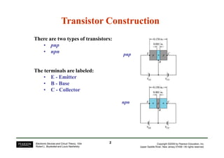
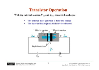
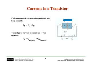
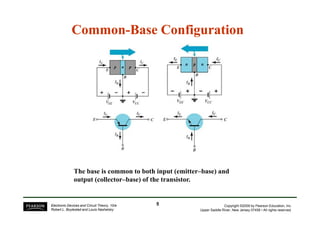
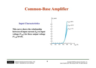
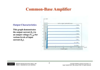
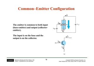
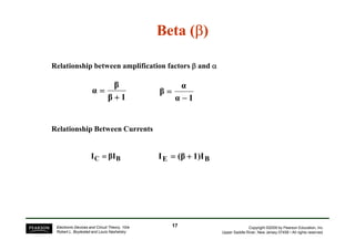
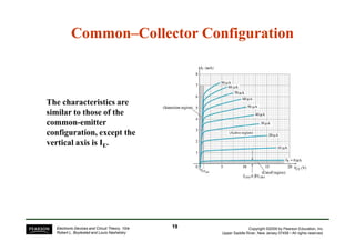
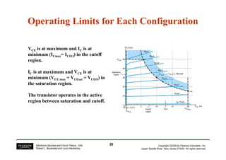
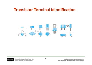
Chapter 3:
Bipolar Junction Transistors
Transistor Construction
There are two types of transistors:
• pnp
• npn
The terminals are labeled:
• E - Emitter
pnp
pnp
Copyright ©2009 by Pearson Education, Inc.
Upper Saddle River, New Jersey 07458 • All rights reserved.
Electronic Devices and Circuit Theory, 10/e
Robert L. Boylestad and Louis Nashelsky
• E - Emitter
• B - Base
• C - Collector
npn
npn
2
2
Transistor Operation
With the external sources, VEE and VCC, connected as shown:
• The emitter-base junction is forward biased
• The base-collector junction is reverse biased
Copyright ©2009 by Pearson Education, Inc.
Upper Saddle River, New Jersey 07458 • All rights reserved.
Electronic Devices and Circuit Theory, 10/e
Robert L. Boylestad and Louis Nashelsky
3
3
Currents in a Transistor
The collector current is comprised of two
B
I
C
I
E
I +
+
+
+
=
=
=
=
Emitter current is the sum of the collector and
base currents:
Copyright ©2009 by Pearson Education, Inc.
Upper Saddle River, New Jersey 07458 • All rights reserved.
Electronic Devices and Circuit Theory, 10/e
Robert L. Boylestad and Louis Nashelsky
The collector current is comprised of two
currents:
minority
CO
I
majority
C
I
C
I +
=
4
4
Common
Common-
-Base Configuration
Base Configuration
Copyright ©2009 by Pearson Education, Inc.
Upper Saddle River, New Jersey 07458 • All rights reserved.
Electronic Devices and Circuit Theory, 10/e
Robert L. Boylestad and Louis Nashelsky
The base is common to both input (emitter–base) and
output (collector–base) of the transistor.
5
5
Common
Common-
-Base Amplifier
Base Amplifier
Input Characteristics
This curve shows the relationship
between of input current (IE) to input
voltage (VBE) for three output voltage
Copyright ©2009 by Pearson Education, Inc.
Upper Saddle River, New Jersey 07458 • All rights reserved.
Electronic Devices and Circuit Theory, 10/e
Robert L. Boylestad and Louis Nashelsky
voltage (VBE) for three output voltage
(VCB) levels.
6
6
This graph demonstrates
the output current (IC) to
an output voltage (VCB) for
Common
Common-
-Base Amplifier
Base Amplifier
Output Characteristics
Copyright ©2009 by Pearson Education, Inc.
Upper Saddle River, New Jersey 07458 • All rights reserved.
Electronic Devices and Circuit Theory, 10/e
Robert L. Boylestad and Louis Nashelsky
an output voltage (VCB) for
various levels of input
current (IE).
7
7
Operating Regions
Operating Regions
• Active – Operating range of the
amplifier.
• Cutoff – The amplifier is basically
off. There is voltage, but little
current.
Copyright ©2009 by Pearson Education, Inc.
Upper Saddle River, New Jersey 07458 • All rights reserved.
Electronic Devices and Circuit Theory, 10/e
Robert L. Boylestad and Louis Nashelsky
current.
•
• Saturation – The amplifier is full on.
There is current, but little voltage.
8
8
E
I
C
I ≅
Approximations
Approximations
Emitter and collector currents:
Base-emitter voltage:
Copyright ©2009 by Pearson Education, Inc.
Upper Saddle River, New Jersey 07458 • All rights reserved.
Electronic Devices and Circuit Theory, 10/e
Robert L. Boylestad and Louis Nashelsky
Silicon)
(for
V
0.7
BE
V =
9
9
Ideally: α
α
α
α = 1
Alpha (
Alpha (α
α
α
α
α
α
α
α)
)
Alpha (α
α
α
α) is the ratio of IC to IE :
E
I
C
I
α =
dc
Copyright ©2009 by Pearson Education, Inc.
Upper Saddle River, New Jersey 07458 • All rights reserved.
Electronic Devices and Circuit Theory, 10/e
Robert L. Boylestad and Louis Nashelsky
Ideally: α
α
α
α = 1
In reality: α
α
α
α is between 0.9 and 0.998
Alpha (α
α
α
α) in the AC mode
AC mode:
E
I
C
I
α
∆
∆
ac =
10
10
Transistor Amplification
Copyright ©2009 by Pearson Education, Inc.
Upper Saddle River, New Jersey 07458 • All rights reserved.
Electronic Devices and Circuit Theory, 10/e
Robert L. Boylestad and Louis Nashelsky
Voltage Gain:
V
50
kΩ
5
ma
10
mA
10
10mA
20Ω
200mV
=
=
=
=
≅
≅
=
=
=
=
)
)(
(
R
L
I
L
V
i
I
L
I
E
I
C
I
i
R
i
V
i
I
E
I
Currents and Voltages:
11
11
250
200mV
50V
=
=
=
i
V
L
V
v
A
Common
Common–
–Emitter Configuration
Emitter Configuration
The emitter is common to both input
(base-emitter) and output (collector-
emitter).
Copyright ©2009 by Pearson Education, Inc.
Upper Saddle River, New Jersey 07458 • All rights reserved.
Electronic Devices and Circuit Theory, 10/e
Robert L. Boylestad and Louis Nashelsky
The input is on the base and the
output is on the collector.
12
12
Common
Common-
-Emitter Characteristics
Emitter Characteristics
Copyright ©2009 by Pearson Education, Inc.
Upper Saddle River, New Jersey 07458 • All rights reserved.
Electronic Devices and Circuit Theory, 10/e
Robert L. Boylestad and Louis Nashelsky
Collector Characteristics Base Characteristics
13
13
Common
Common-
-Emitter Amplifier Currents
Emitter Amplifier Currents
Ideal Currents
Ideal Currents
IE = IC + IB IC = α
α
α
α IE
Actual Currents
Actual Currents
IC = α
α
α
α IE + ICBO where ICBO = minority collector current
Copyright ©2009 by Pearson Education, Inc.
Upper Saddle River, New Jersey 07458 • All rights reserved.
Electronic Devices and Circuit Theory, 10/e
Robert L. Boylestad and Louis Nashelsky
IC = α
α
α
α IE + ICBO
When IB = 0 µ
µ
µ
µA the transistor is in cutoff, but there is some minority
current flowing called ICEO.
µA
0
=
−
= B
I
CBO
CEO
α
I
I
1
where ICBO = minority collector current
14
14
ICBO is usually so small that it can be ignored, except in high
power transistors and in high temperature environments.
Beta (
Beta (β
β
β
β
β
β
β
β)
)
In DC mode:
β
β
β
β represents the amplification factor of a transistor. (β
β
β
β is
sometimes referred to as hfe, a term used in transistor modeling
calculations)
C
I
β =
dc
Copyright ©2009 by Pearson Education, Inc.
Upper Saddle River, New Jersey 07458 • All rights reserved.
Electronic Devices and Circuit Theory, 10/e
Robert L. Boylestad and Louis Nashelsky
In AC mode:
B
I
β =
dc
constant
ac =
∆
∆
= CE
V
B
C
I
I
β
15
15
Determining β
β
β
β from a Graph
Beta (
Beta (β
β
β
β
β
β
β
β)
)
100
µA
10
mA
1
µA)
20
µA
(30
mA)
2.2
mA
(3.2
β
7.5
V
AC
CE
=
=
=
=
=
=
=
=
−
−
−
−
−
−
−
−
=
=
=
=
=
=
=
=
Copyright ©2009 by Pearson Education, Inc.
Upper Saddle River, New Jersey 07458 • All rights reserved.
Electronic Devices and Circuit Theory, 10/e
Robert L. Boylestad and Louis Nashelsky
108
A
25
mA
2.7
β 7.5
V
DC CE
=
=
=
=
µ
µ
µ
µ
=
=
=
= =
=
=
=
100
=
=
=
=
16
16
Relationship between amplification factors β
β
β
β and α
α
α
α
1
β
β
α
+
+
+
+
=
=
=
=
1
α
α
β
−
−
−
−
=
=
=
=
Beta (
Beta (β
β
β
β
β
β
β
β)
)
Relationship Between Currents
Copyright ©2009 by Pearson Education, Inc.
Upper Saddle River, New Jersey 07458 • All rights reserved.
Electronic Devices and Circuit Theory, 10/e
Robert L. Boylestad and Louis Nashelsky
Relationship Between Currents
B
C βI
I =
=
=
= B
E 1)I
(β
I +
+
+
+
=
=
=
=
17
17
Common
Common–
–Collector Configuration
Collector Configuration
The input is on the
base and the output is
on the emitter.
Copyright ©2009 by Pearson Education, Inc.
Upper Saddle River, New Jersey 07458 • All rights reserved.
Electronic Devices and Circuit Theory, 10/e
Robert L. Boylestad and Louis Nashelsky
18
18
Common
Common–
–Collector Configuration
Collector Configuration
The characteristics are
similar to those of the
common-emitter
Copyright ©2009 by Pearson Education, Inc.
Upper Saddle River, New Jersey 07458 • All rights reserved.
Electronic Devices and Circuit Theory, 10/e
Robert L. Boylestad and Louis Nashelsky
common-emitter
configuration, except the
vertical axis is IE.
19
19
VCE is at maximum and IC is at
minimum (ICmax= ICEO) in the cutoff
region.
IC is at maximum and VCE is at
minimum (VCE max = VCEsat = VCEO) in
Operating Limits for Each Configuration
Copyright ©2009 by Pearson Education, Inc.
Upper Saddle River, New Jersey 07458 • All rights reserved.
Electronic Devices and Circuit Theory, 10/e
Robert L. Boylestad and Louis Nashelsky
minimum (VCE max = VCEsat = VCEO) in
the saturation region.
The transistor operates in the active
region between saturation and cutoff.
20
20
Power Dissipation
Power Dissipation
C
CB
Cmax I
V
P =
=
=
=
C
CE
Cmax I
V
P =
=
=
=
Common-base:
Common-emitter:
Copyright ©2009 by Pearson Education, Inc.
Upper Saddle River, New Jersey 07458 • All rights reserved.
Electronic Devices and Circuit Theory, 10/e
Robert L. Boylestad and Louis Nashelsky
Common-collector:
E
CE
Cmax I
V
P =
=
=
=
21
21
Transistor Specification Sheet
Copyright ©2009 by Pearson Education, Inc.
Upper Saddle River, New Jersey 07458 • All rights reserved.
Electronic Devices and Circuit Theory, 10/e
Robert L. Boylestad and Louis Nashelsky
22
22
Transistor Specification Sheet
Copyright ©2009 by Pearson Education, Inc.
Upper Saddle River, New Jersey 07458 • All rights reserved.
Electronic Devices and Circuit Theory, 10/e
Robert L. Boylestad and Louis Nashelsky
23
23
Transistor Testing
Transistor Testing
•
• Curve Tracer
Curve Tracer
Provides a graph of the characteristic curves.
•
• DMM
DMM
Some DMMs measure β
β
β
βDC or hFE.
•
• Ohmmeter
Ohmmeter
Copyright ©2009 by Pearson Education, Inc.
Upper Saddle River, New Jersey 07458 • All rights reserved.
Electronic Devices and Circuit Theory, 10/e
Robert L. Boylestad and Louis Nashelsky
24
24
Transistor Terminal Identification
Copyright ©2009 by Pearson Education, Inc.
Upper Saddle River, New Jersey 07458 • All rights reserved.
Electronic Devices and Circuit Theory, 10/e
Robert L. Boylestad and Louis Nashelsky
25
25

Bem (6)

  • 1.
  • 2.
    Transistor Construction Transistor Construction Thereare two types of transistors: • pnp • npn The terminals are labeled: • E - Emitter pnp pnp Copyright ©2009 by Pearson Education, Inc. Upper Saddle River, New Jersey 07458 • All rights reserved. Electronic Devices and Circuit Theory, 10/e Robert L. Boylestad and Louis Nashelsky • E - Emitter • B - Base • C - Collector npn npn 2 2
  • 3.
    Transistor Operation Transistor Operation Withthe external sources, VEE and VCC, connected as shown: • The emitter-base junction is forward biased • The base-collector junction is reverse biased Copyright ©2009 by Pearson Education, Inc. Upper Saddle River, New Jersey 07458 • All rights reserved. Electronic Devices and Circuit Theory, 10/e Robert L. Boylestad and Louis Nashelsky 3 3
  • 4.
    Currents in aTransistor Currents in a Transistor The collector current is comprised of two B I C I E I + + + + = = = = Emitter current is the sum of the collector and base currents: Copyright ©2009 by Pearson Education, Inc. Upper Saddle River, New Jersey 07458 • All rights reserved. Electronic Devices and Circuit Theory, 10/e Robert L. Boylestad and Louis Nashelsky The collector current is comprised of two currents: minority CO I majority C I C I + = 4 4
  • 5.
    Common Common- -Base Configuration Base Configuration Copyright©2009 by Pearson Education, Inc. Upper Saddle River, New Jersey 07458 • All rights reserved. Electronic Devices and Circuit Theory, 10/e Robert L. Boylestad and Louis Nashelsky The base is common to both input (emitter–base) and output (collector–base) of the transistor. 5 5
  • 6.
    Common Common- -Base Amplifier Base Amplifier InputCharacteristics Input Characteristics This curve shows the relationship between of input current (IE) to input voltage (VBE) for three output voltage Copyright ©2009 by Pearson Education, Inc. Upper Saddle River, New Jersey 07458 • All rights reserved. Electronic Devices and Circuit Theory, 10/e Robert L. Boylestad and Louis Nashelsky voltage (VBE) for three output voltage (VCB) levels. 6 6
  • 7.
    This graph demonstrates theoutput current (IC) to an output voltage (VCB) for Common Common- -Base Amplifier Base Amplifier Output Characteristics Output Characteristics Copyright ©2009 by Pearson Education, Inc. Upper Saddle River, New Jersey 07458 • All rights reserved. Electronic Devices and Circuit Theory, 10/e Robert L. Boylestad and Louis Nashelsky an output voltage (VCB) for various levels of input current (IE). 7 7
  • 8.
    Operating Regions Operating Regions •Active – Operating range of the amplifier. • Cutoff – The amplifier is basically off. There is voltage, but little current. Copyright ©2009 by Pearson Education, Inc. Upper Saddle River, New Jersey 07458 • All rights reserved. Electronic Devices and Circuit Theory, 10/e Robert L. Boylestad and Louis Nashelsky current. • • Saturation – The amplifier is full on. There is current, but little voltage. 8 8
  • 9.
    E I C I ≅ Approximations Approximations Emitter andcollector currents: Base-emitter voltage: Copyright ©2009 by Pearson Education, Inc. Upper Saddle River, New Jersey 07458 • All rights reserved. Electronic Devices and Circuit Theory, 10/e Robert L. Boylestad and Louis Nashelsky Silicon) (for V 0.7 BE V = 9 9
  • 10.
    Ideally: α α α α =1 Alpha ( Alpha (α α α α α α α α) ) Alpha (α α α α) is the ratio of IC to IE : E I C I α = dc Copyright ©2009 by Pearson Education, Inc. Upper Saddle River, New Jersey 07458 • All rights reserved. Electronic Devices and Circuit Theory, 10/e Robert L. Boylestad and Louis Nashelsky Ideally: α α α α = 1 In reality: α α α α is between 0.9 and 0.998 Alpha (α α α α) in the AC mode AC mode: E I C I α ∆ ∆ ac = 10 10
  • 11.
    Transistor Amplification Transistor Amplification Copyright©2009 by Pearson Education, Inc. Upper Saddle River, New Jersey 07458 • All rights reserved. Electronic Devices and Circuit Theory, 10/e Robert L. Boylestad and Louis Nashelsky Voltage Gain: V 50 kΩ 5 ma 10 mA 10 10mA 20Ω 200mV = = = = ≅ ≅ = = = = ) )( ( R L I L V i I L I E I C I i R i V i I E I Currents and Voltages: 11 11 250 200mV 50V = = = i V L V v A
  • 12.
    Common Common– –Emitter Configuration Emitter Configuration Theemitter is common to both input (base-emitter) and output (collector- emitter). Copyright ©2009 by Pearson Education, Inc. Upper Saddle River, New Jersey 07458 • All rights reserved. Electronic Devices and Circuit Theory, 10/e Robert L. Boylestad and Louis Nashelsky The input is on the base and the output is on the collector. 12 12
  • 13.
    Common Common- -Emitter Characteristics Emitter Characteristics Copyright©2009 by Pearson Education, Inc. Upper Saddle River, New Jersey 07458 • All rights reserved. Electronic Devices and Circuit Theory, 10/e Robert L. Boylestad and Louis Nashelsky Collector Characteristics Base Characteristics 13 13
  • 14.
    Common Common- -Emitter Amplifier Currents EmitterAmplifier Currents Ideal Currents Ideal Currents IE = IC + IB IC = α α α α IE Actual Currents Actual Currents IC = α α α α IE + ICBO where ICBO = minority collector current Copyright ©2009 by Pearson Education, Inc. Upper Saddle River, New Jersey 07458 • All rights reserved. Electronic Devices and Circuit Theory, 10/e Robert L. Boylestad and Louis Nashelsky IC = α α α α IE + ICBO When IB = 0 µ µ µ µA the transistor is in cutoff, but there is some minority current flowing called ICEO. µA 0 = − = B I CBO CEO α I I 1 where ICBO = minority collector current 14 14 ICBO is usually so small that it can be ignored, except in high power transistors and in high temperature environments.
  • 15.
    Beta ( Beta (β β β β β β β β) ) InDC mode: β β β β represents the amplification factor of a transistor. (β β β β is sometimes referred to as hfe, a term used in transistor modeling calculations) C I β = dc Copyright ©2009 by Pearson Education, Inc. Upper Saddle River, New Jersey 07458 • All rights reserved. Electronic Devices and Circuit Theory, 10/e Robert L. Boylestad and Louis Nashelsky In AC mode: B I β = dc constant ac = ∆ ∆ = CE V B C I I β 15 15
  • 16.
    Determining β β β β froma Graph Beta ( Beta (β β β β β β β β) ) 100 µA 10 mA 1 µA) 20 µA (30 mA) 2.2 mA (3.2 β 7.5 V AC CE = = = = = = = = − − − − − − − − = = = = = = = = Copyright ©2009 by Pearson Education, Inc. Upper Saddle River, New Jersey 07458 • All rights reserved. Electronic Devices and Circuit Theory, 10/e Robert L. Boylestad and Louis Nashelsky 108 A 25 mA 2.7 β 7.5 V DC CE = = = = µ µ µ µ = = = = = = = = 100 = = = = 16 16
  • 17.
    Relationship between amplificationfactors β β β β and α α α α 1 β β α + + + + = = = = 1 α α β − − − − = = = = Beta ( Beta (β β β β β β β β) ) Relationship Between Currents Copyright ©2009 by Pearson Education, Inc. Upper Saddle River, New Jersey 07458 • All rights reserved. Electronic Devices and Circuit Theory, 10/e Robert L. Boylestad and Louis Nashelsky Relationship Between Currents B C βI I = = = = B E 1)I (β I + + + + = = = = 17 17
  • 18.
    Common Common– –Collector Configuration Collector Configuration Theinput is on the base and the output is on the emitter. Copyright ©2009 by Pearson Education, Inc. Upper Saddle River, New Jersey 07458 • All rights reserved. Electronic Devices and Circuit Theory, 10/e Robert L. Boylestad and Louis Nashelsky 18 18
  • 19.
    Common Common– –Collector Configuration Collector Configuration Thecharacteristics are similar to those of the common-emitter Copyright ©2009 by Pearson Education, Inc. Upper Saddle River, New Jersey 07458 • All rights reserved. Electronic Devices and Circuit Theory, 10/e Robert L. Boylestad and Louis Nashelsky common-emitter configuration, except the vertical axis is IE. 19 19
  • 20.
    VCE is atmaximum and IC is at minimum (ICmax= ICEO) in the cutoff region. IC is at maximum and VCE is at minimum (VCE max = VCEsat = VCEO) in Operating Limits for Each Configuration Operating Limits for Each Configuration Copyright ©2009 by Pearson Education, Inc. Upper Saddle River, New Jersey 07458 • All rights reserved. Electronic Devices and Circuit Theory, 10/e Robert L. Boylestad and Louis Nashelsky minimum (VCE max = VCEsat = VCEO) in the saturation region. The transistor operates in the active region between saturation and cutoff. 20 20
  • 21.
    Power Dissipation Power Dissipation C CB CmaxI V P = = = = C CE Cmax I V P = = = = Common-base: Common-emitter: Copyright ©2009 by Pearson Education, Inc. Upper Saddle River, New Jersey 07458 • All rights reserved. Electronic Devices and Circuit Theory, 10/e Robert L. Boylestad and Louis Nashelsky Common-collector: E CE Cmax I V P = = = = 21 21
  • 22.
    Transistor Specification Sheet TransistorSpecification Sheet Copyright ©2009 by Pearson Education, Inc. Upper Saddle River, New Jersey 07458 • All rights reserved. Electronic Devices and Circuit Theory, 10/e Robert L. Boylestad and Louis Nashelsky 22 22
  • 23.
    Transistor Specification Sheet TransistorSpecification Sheet Copyright ©2009 by Pearson Education, Inc. Upper Saddle River, New Jersey 07458 • All rights reserved. Electronic Devices and Circuit Theory, 10/e Robert L. Boylestad and Louis Nashelsky 23 23
  • 24.
    Transistor Testing Transistor Testing • •Curve Tracer Curve Tracer Provides a graph of the characteristic curves. • • DMM DMM Some DMMs measure β β β βDC or hFE. • • Ohmmeter Ohmmeter Copyright ©2009 by Pearson Education, Inc. Upper Saddle River, New Jersey 07458 • All rights reserved. Electronic Devices and Circuit Theory, 10/e Robert L. Boylestad and Louis Nashelsky 24 24
  • 25.
    Transistor Terminal Identification TransistorTerminal Identification Copyright ©2009 by Pearson Education, Inc. Upper Saddle River, New Jersey 07458 • All rights reserved. Electronic Devices and Circuit Theory, 10/e Robert L. Boylestad and Louis Nashelsky 25 25