Download as PDF, PPTX

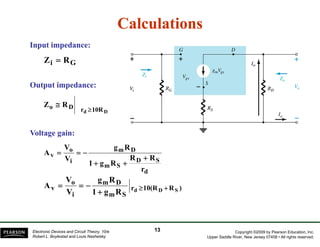
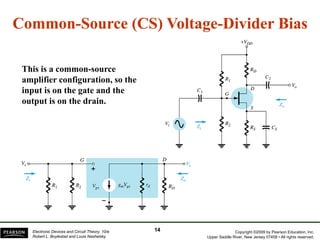
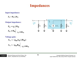
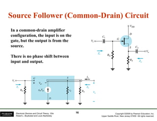
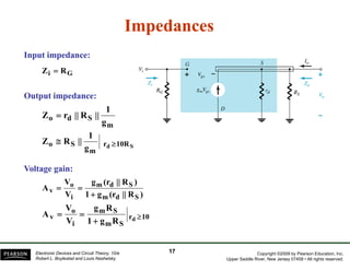
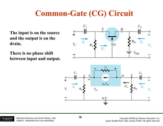
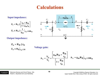
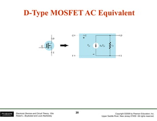

The document discusses field-effect transistors (FETs) and FET amplifiers. It describes the basic FET configurations including common-source, common-gate, and common-drain. It provides the small-signal models and calculations for voltage gain, input and output impedances for each configuration. Additional topics covered include biasing techniques, MOSFET models, and troubleshooting FET amplifiers.


![[Deck] What's New in Spark-Iceberg Integration via DSV2.pptx](https://cdn.slidesharecdn.com/ss_thumbnails/deckwhatsnewinspark-icebergintegrationviadsv2-260210005337-25955b12-thumbnail.jpg?width=640&height=640&fit=bounds)


