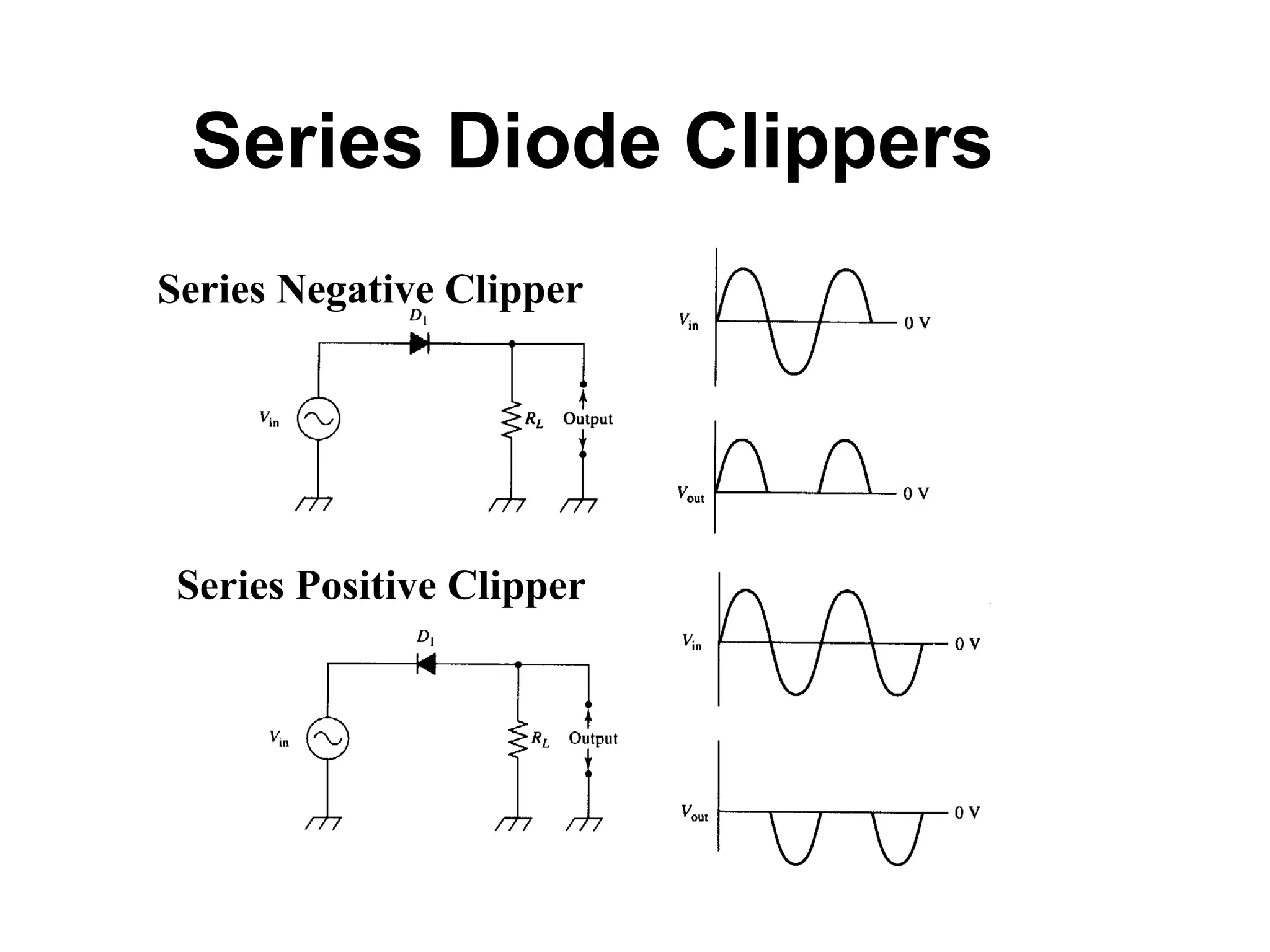
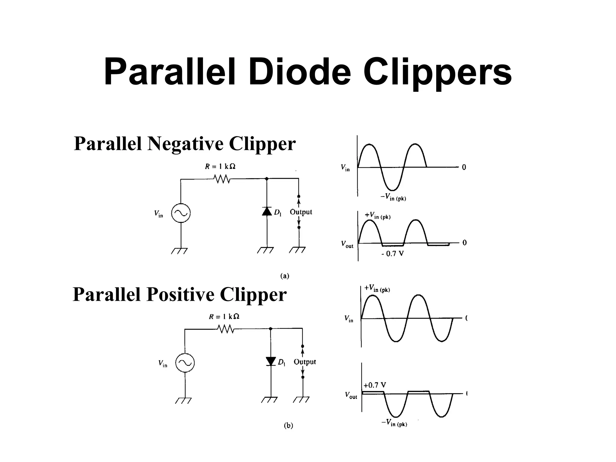
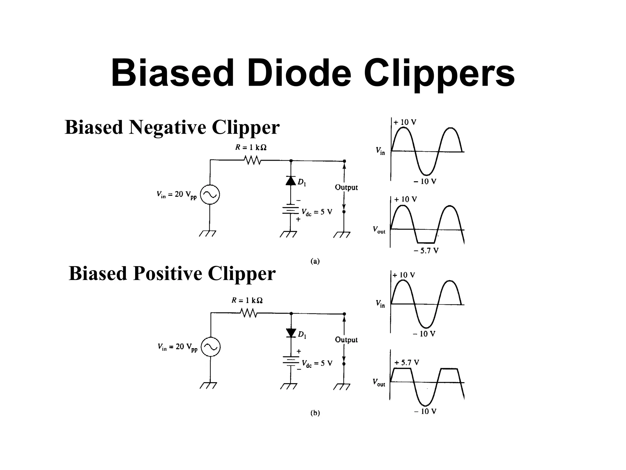
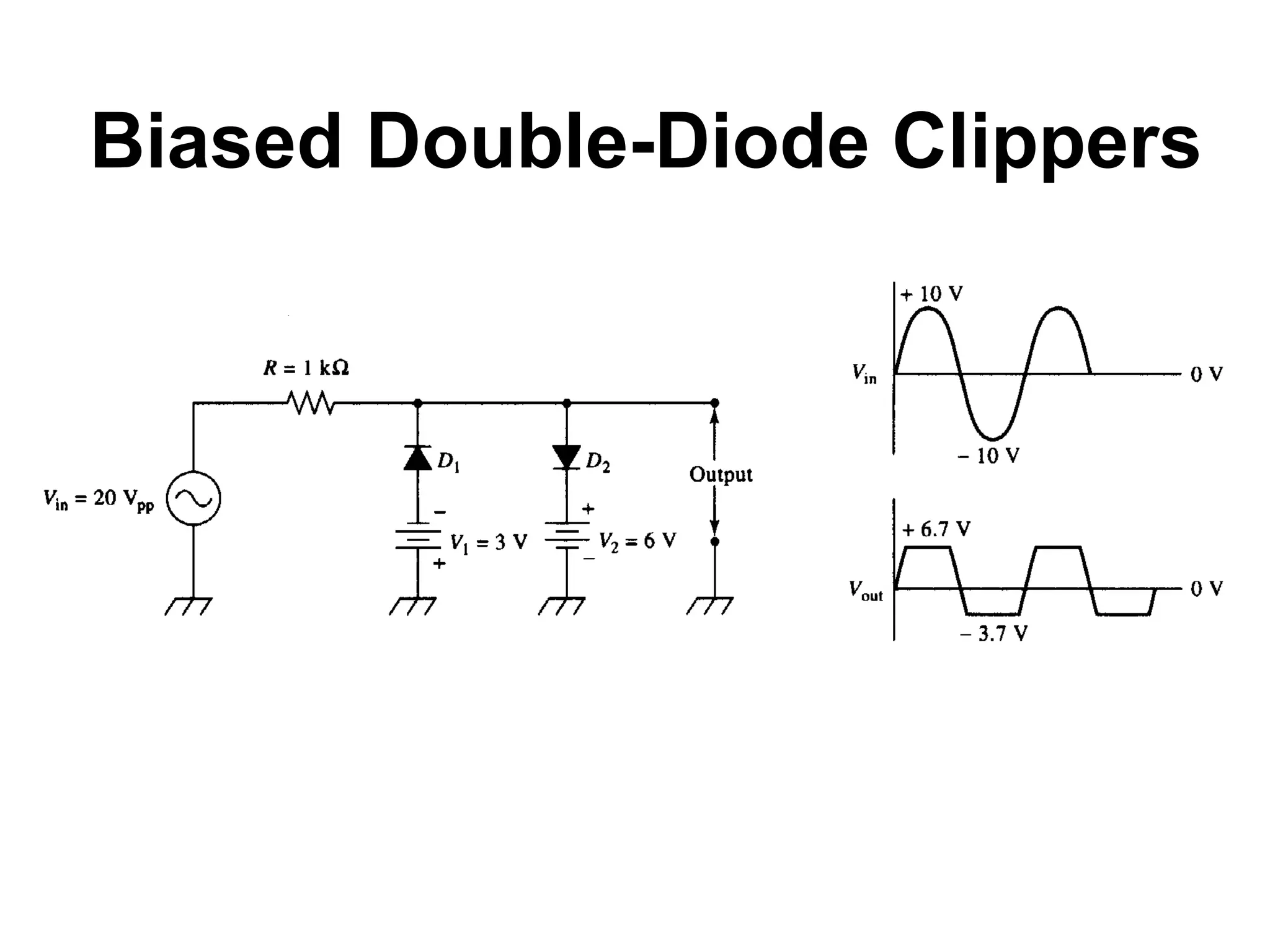
This document provides information on various topics related to semiconductor devices and transistor amplifiers, including:
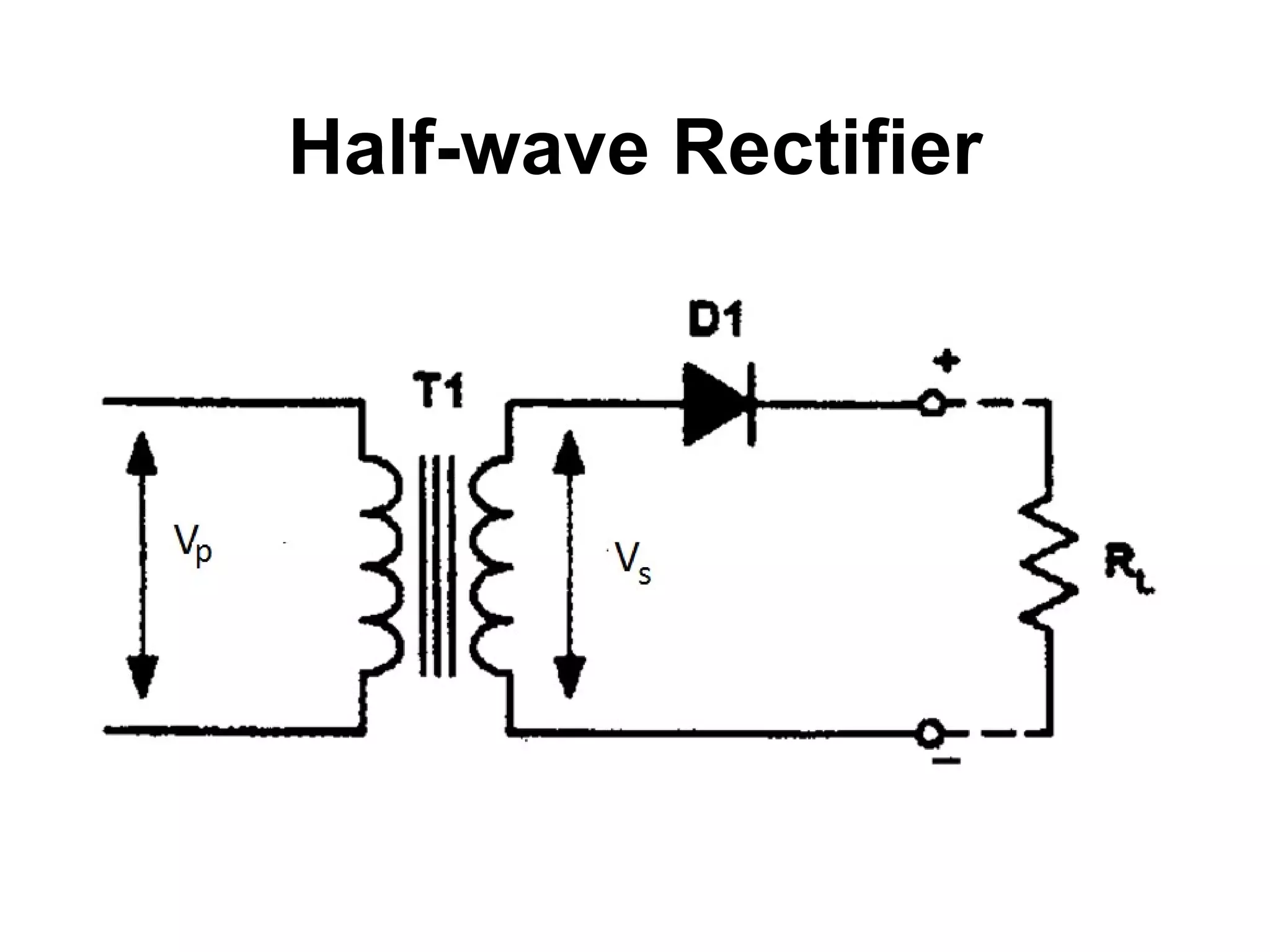
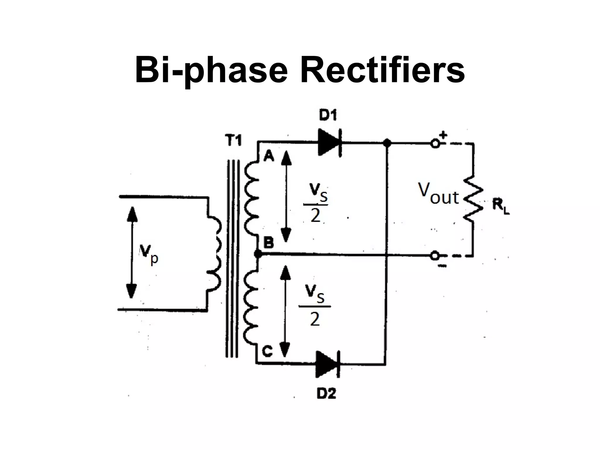
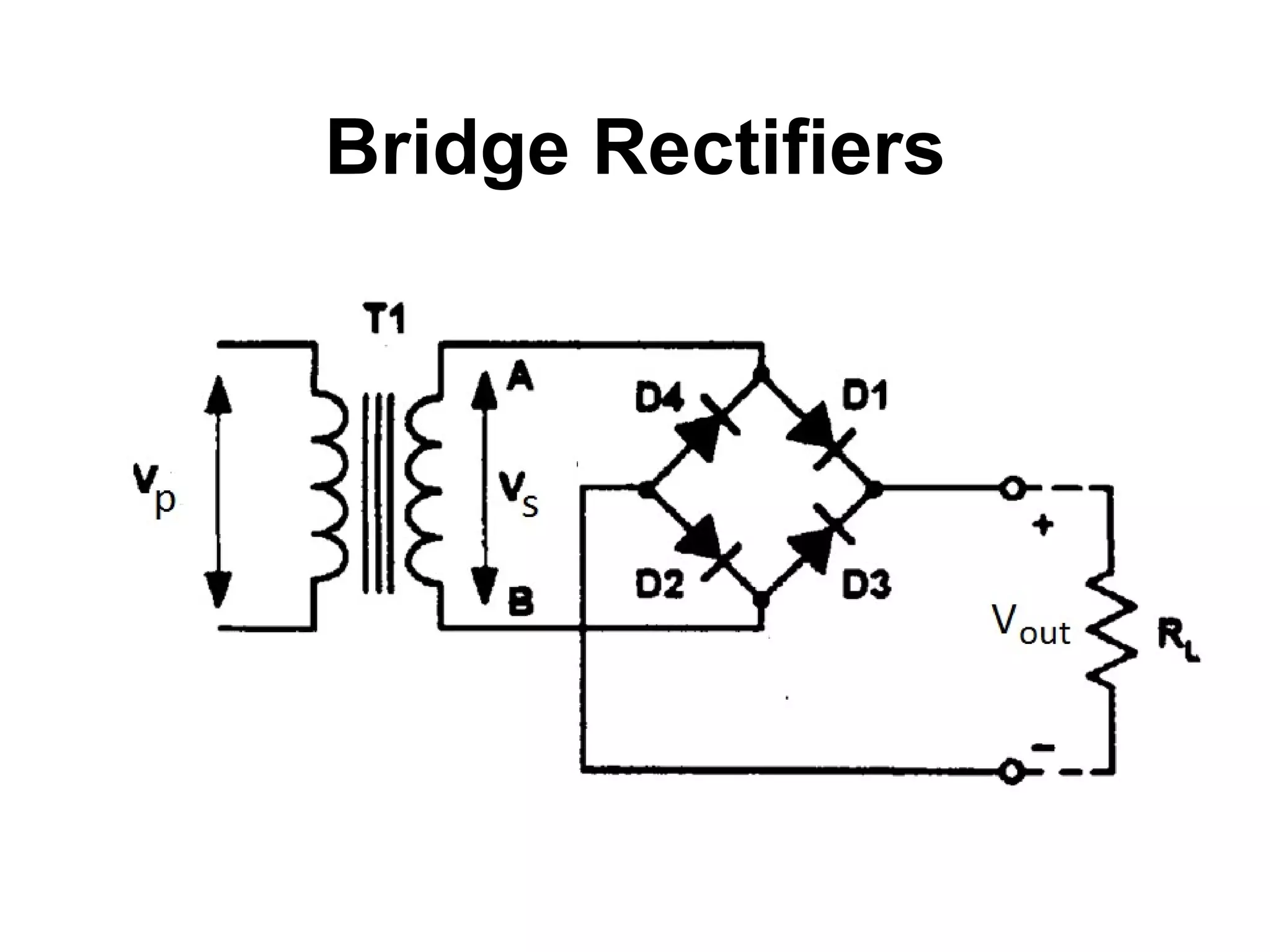
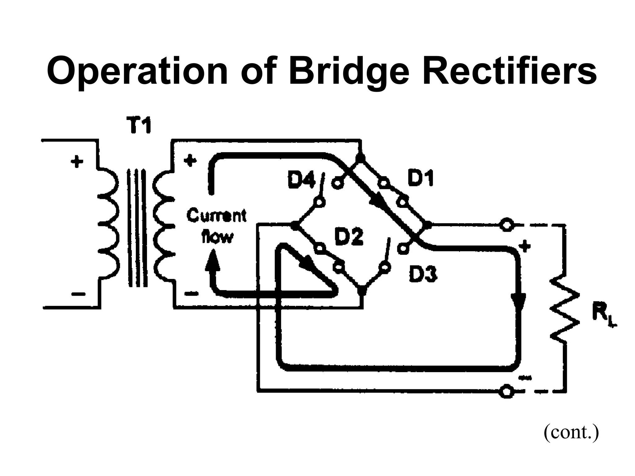
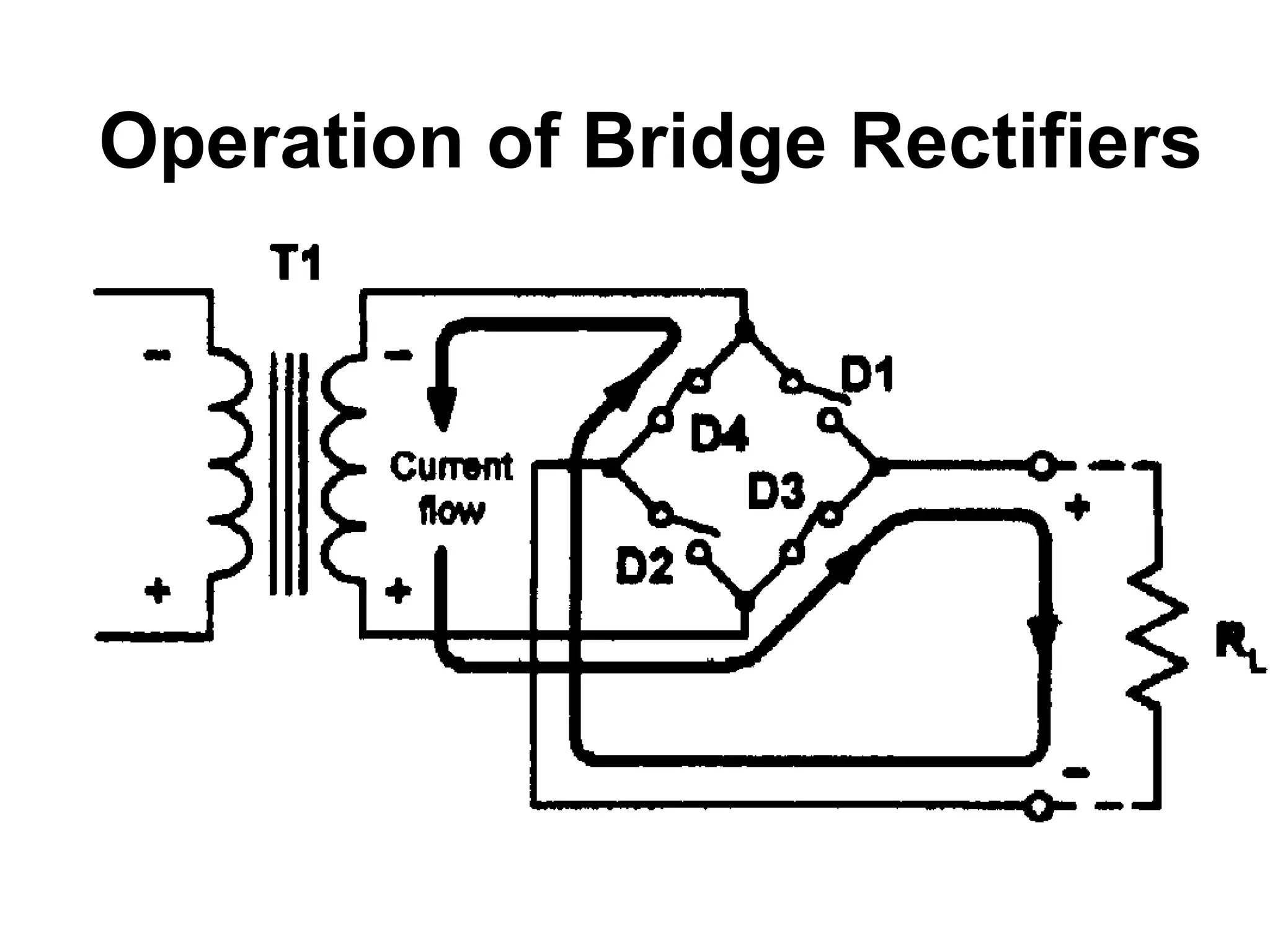
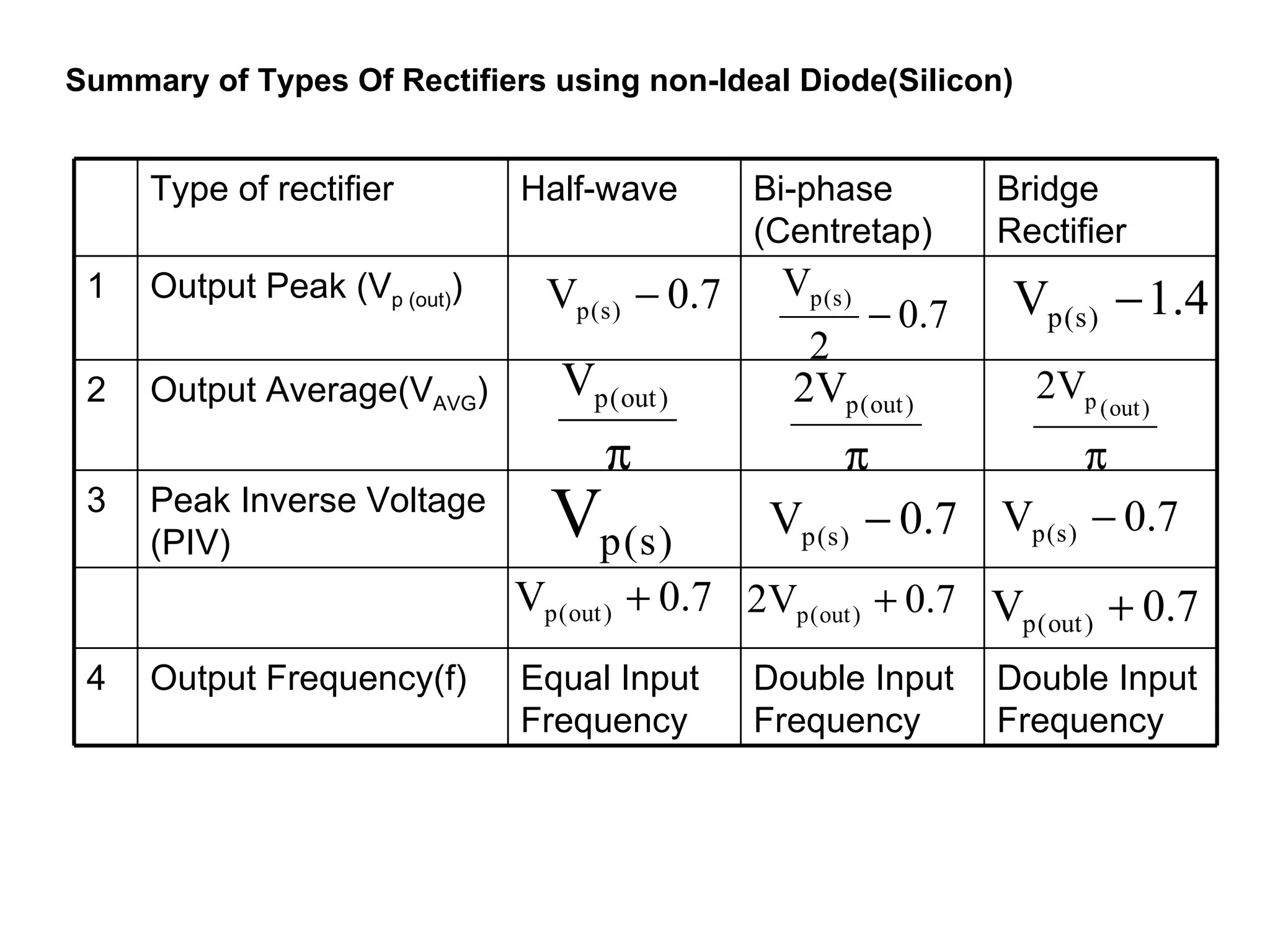
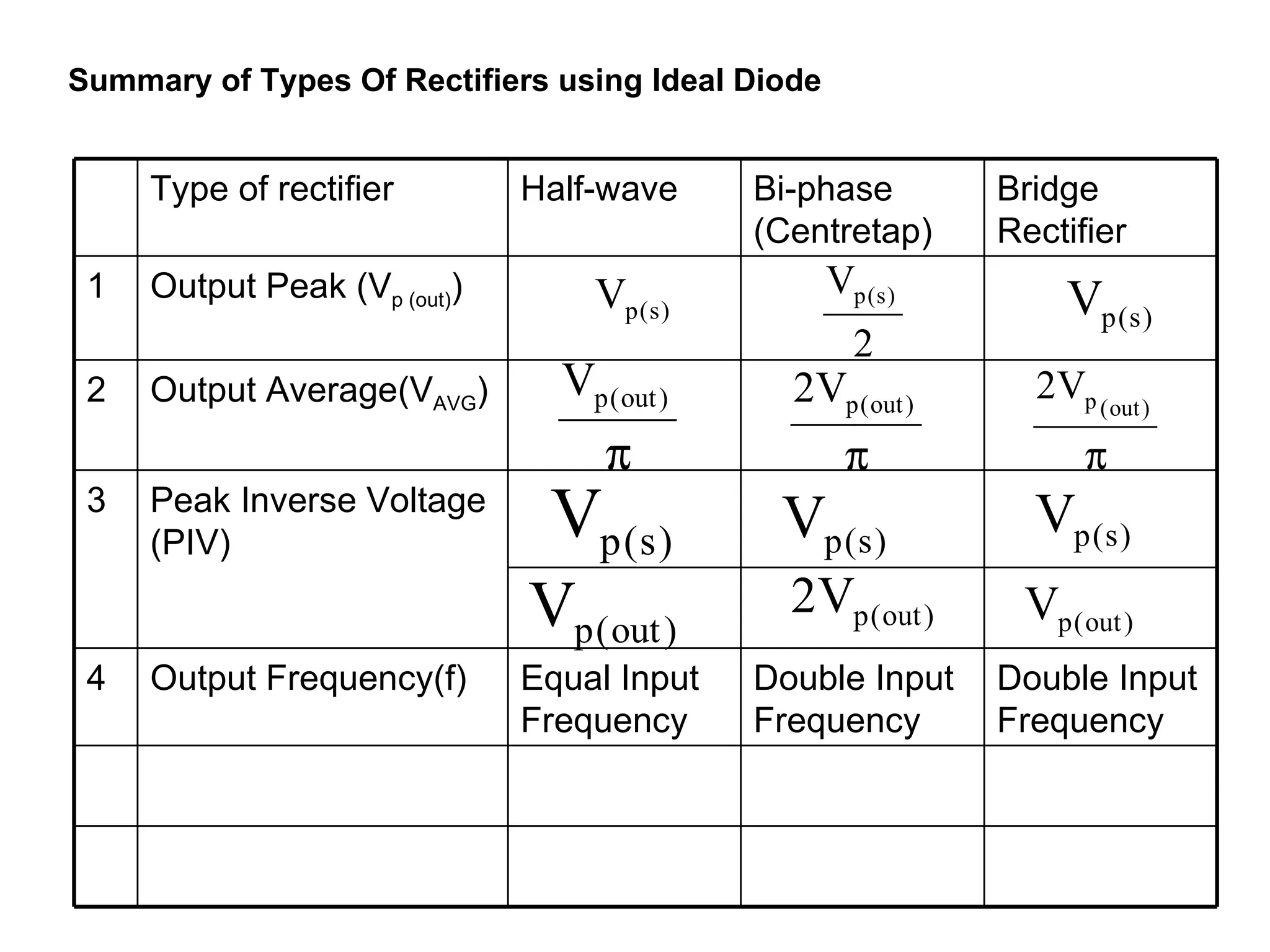
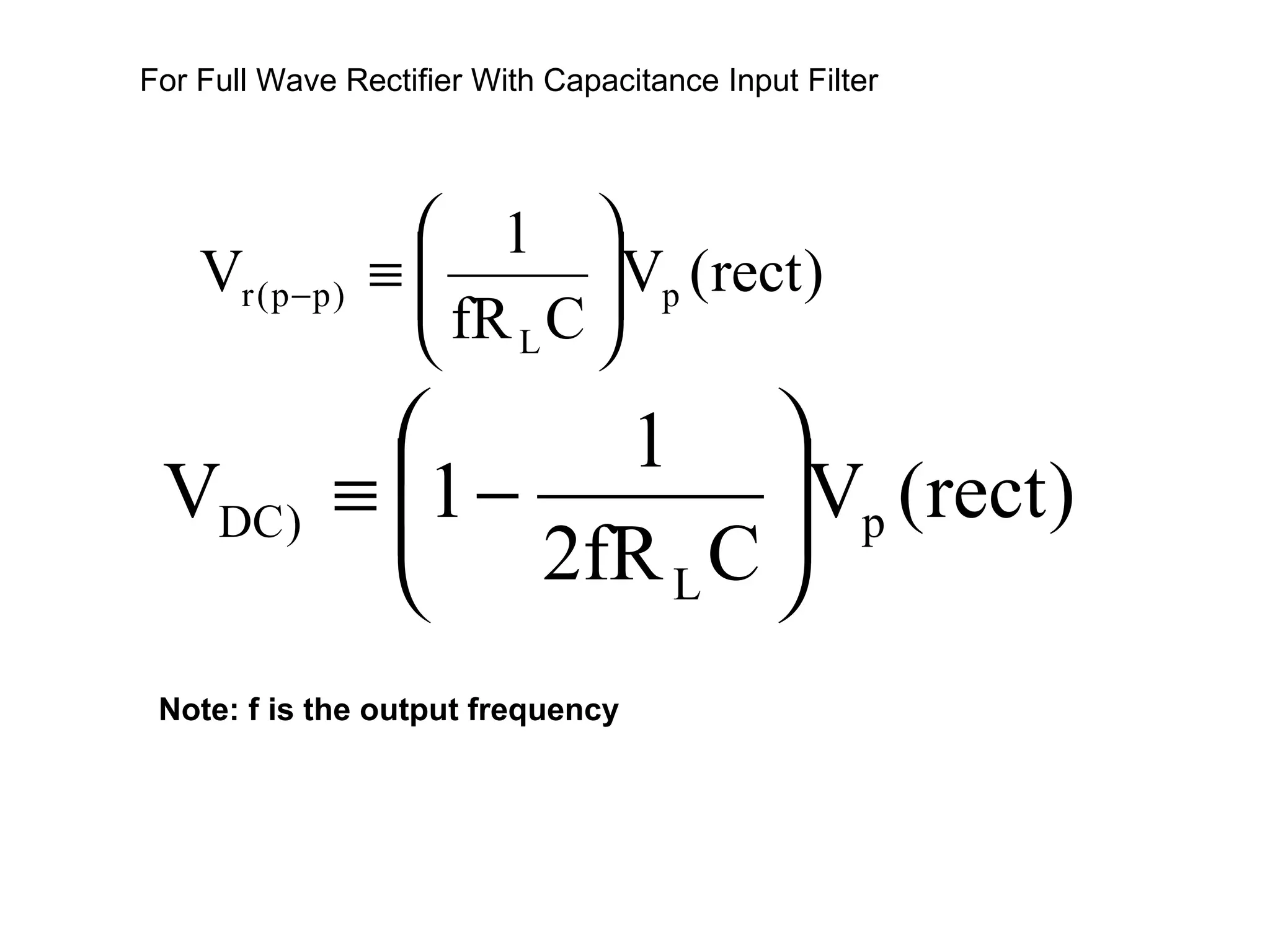
- Types of rectifiers such as half-wave, full-wave, and bridge rectifiers.
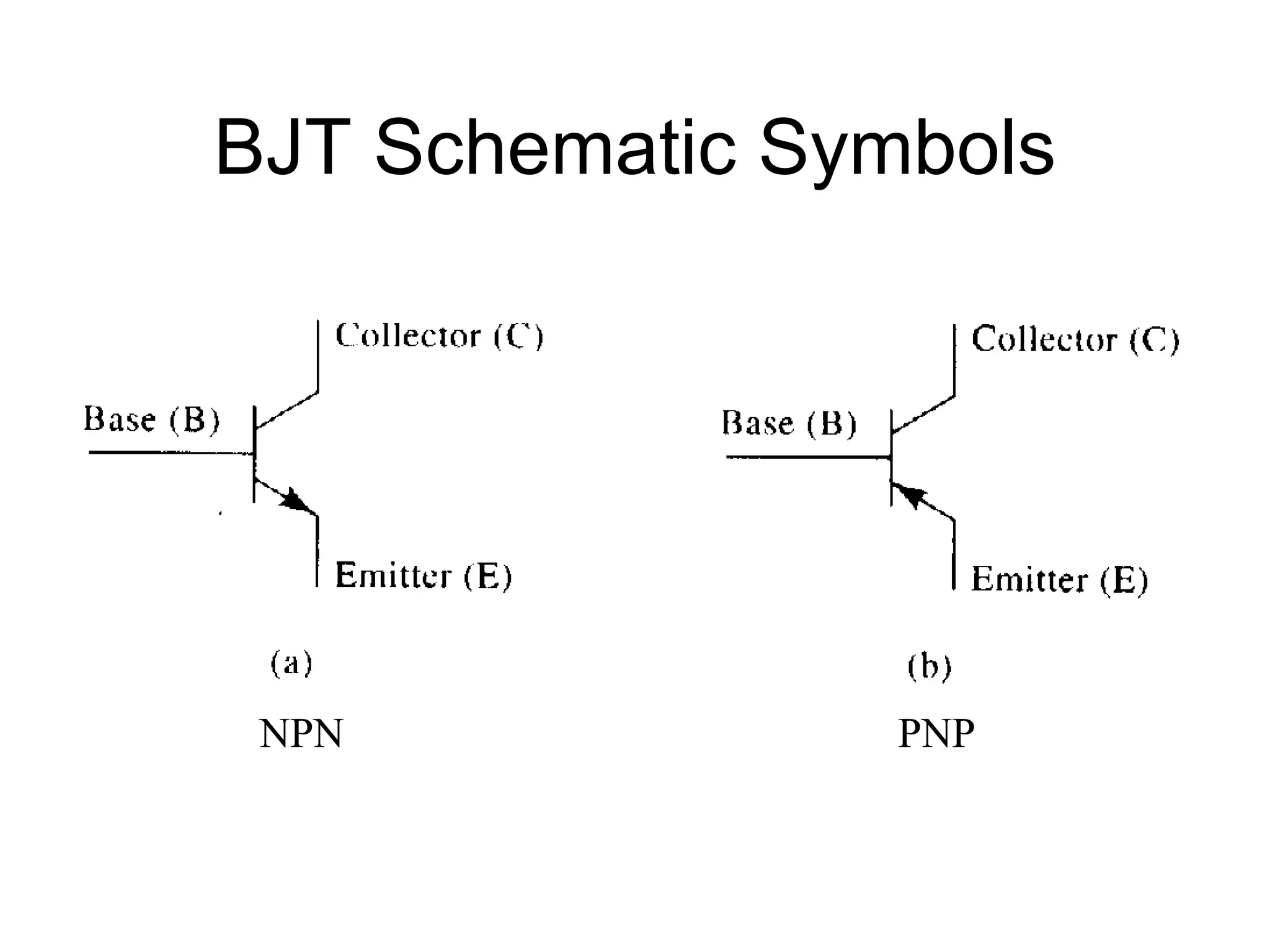
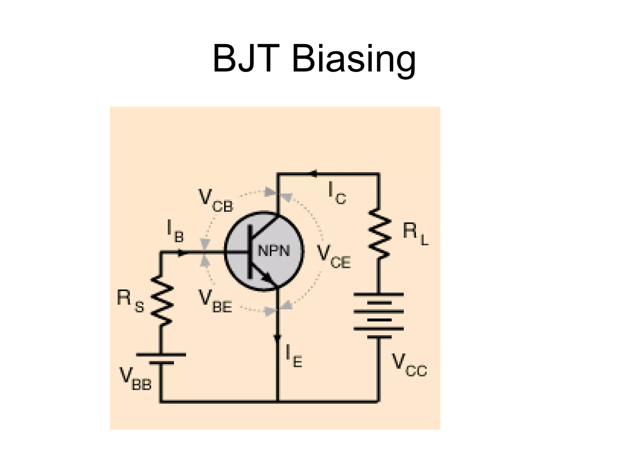
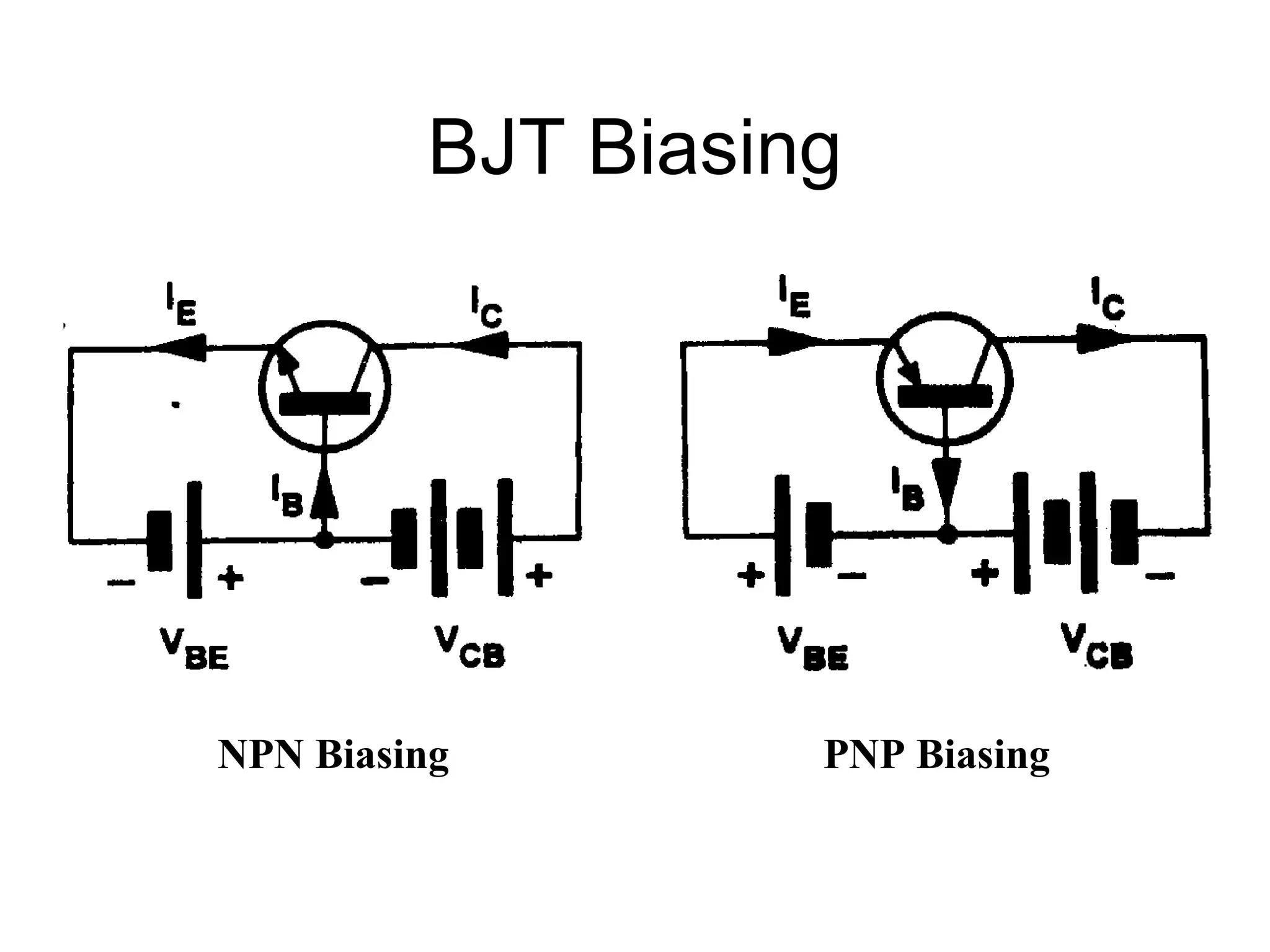
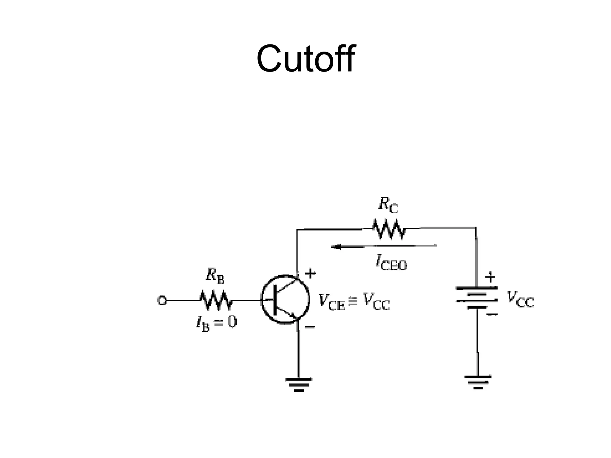
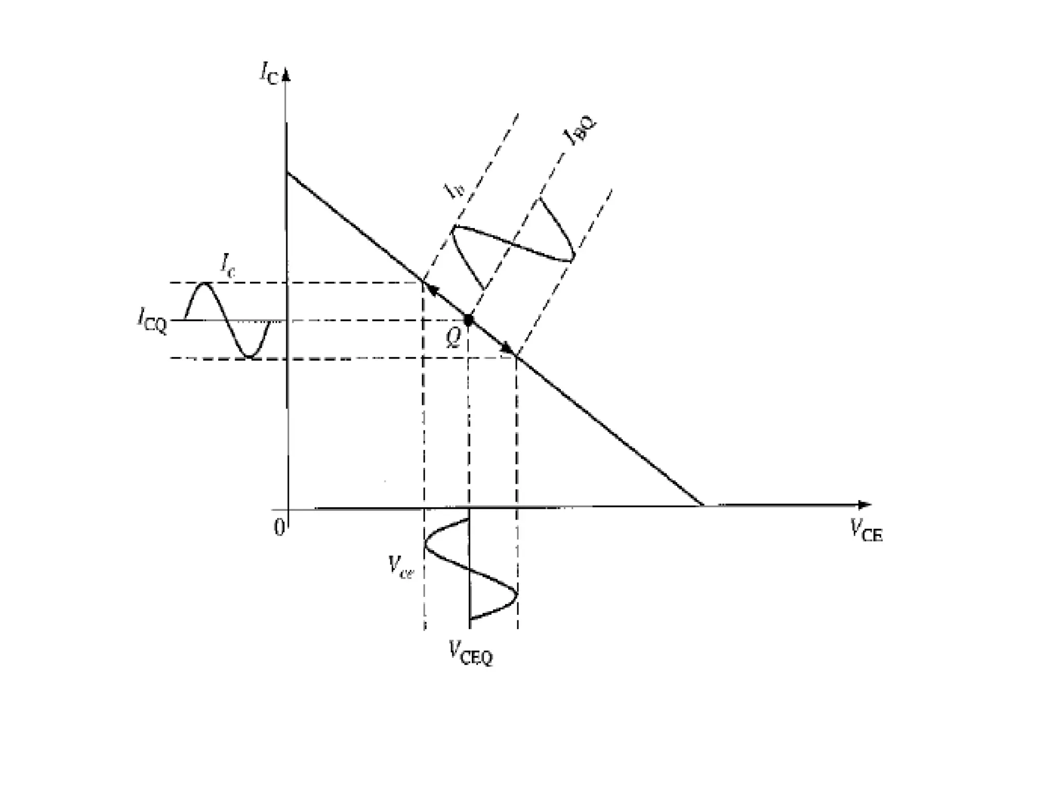
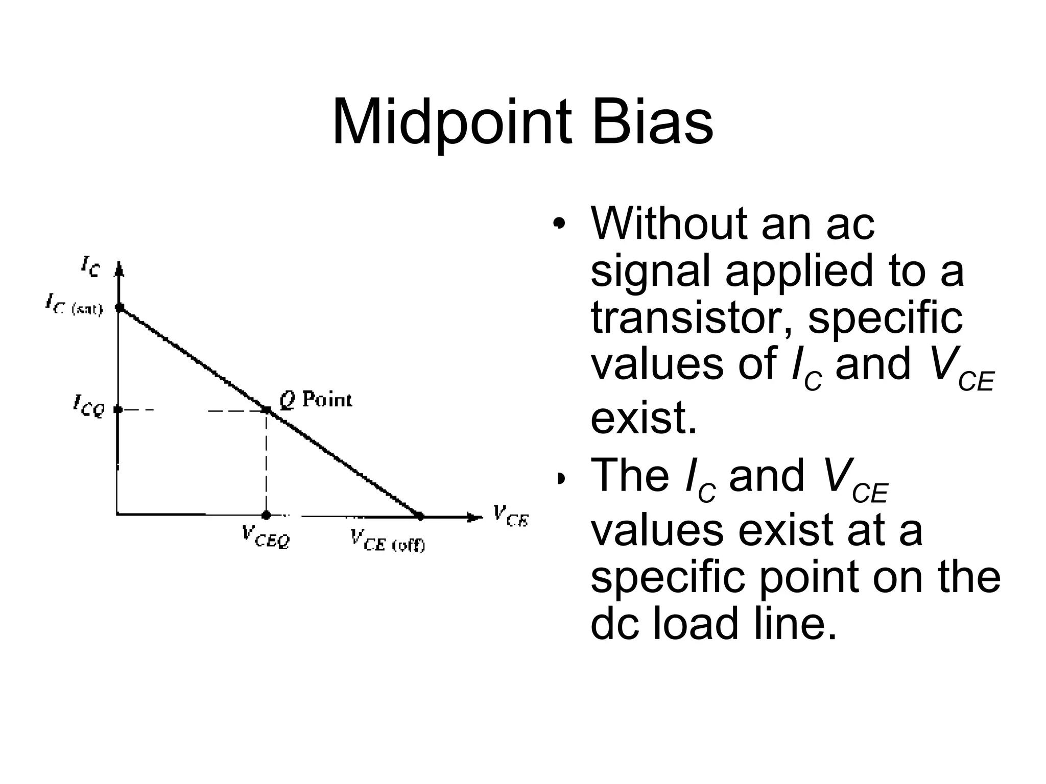
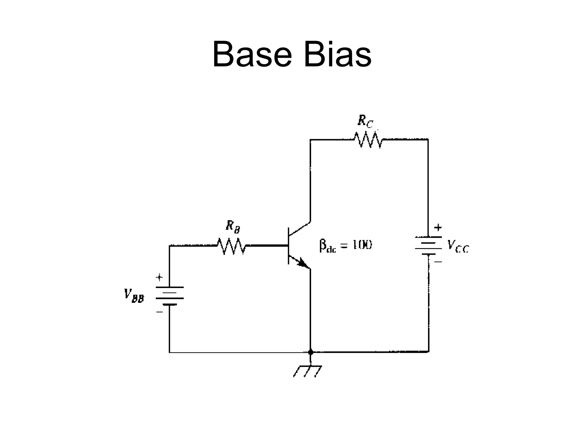
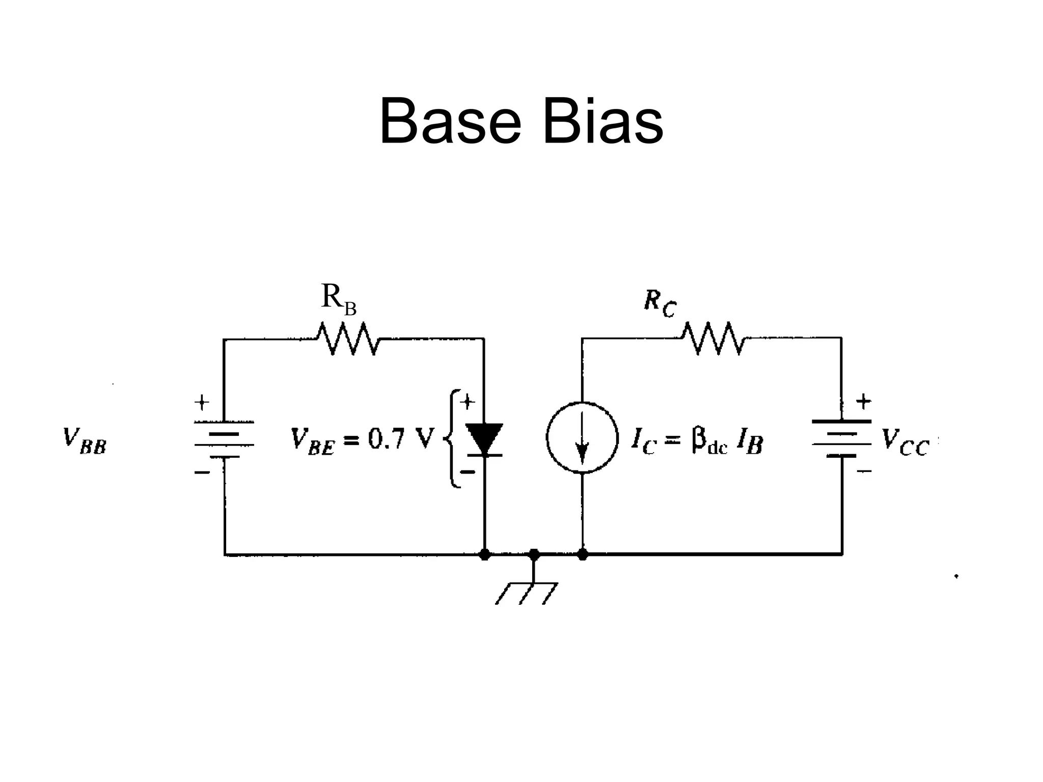
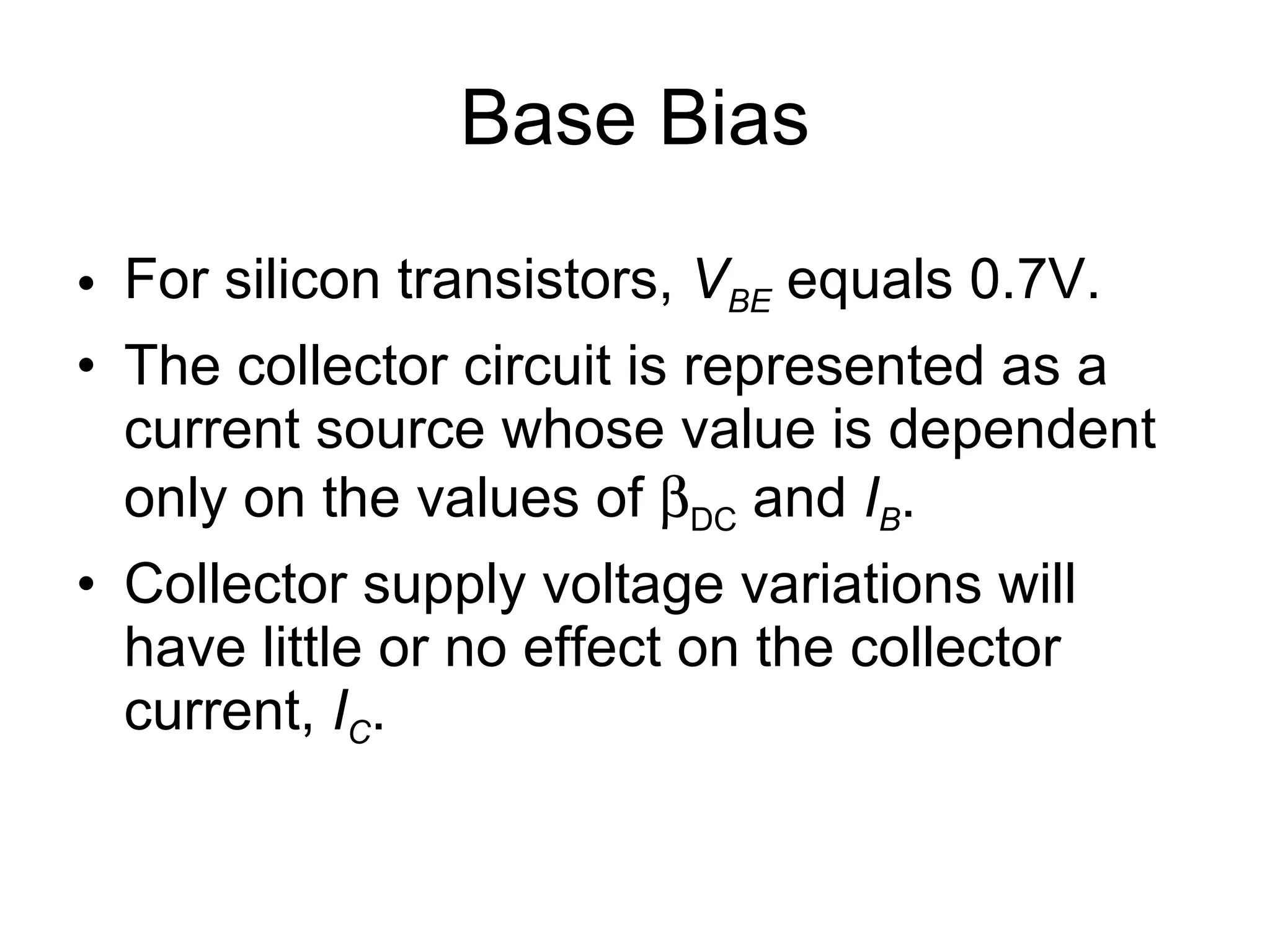
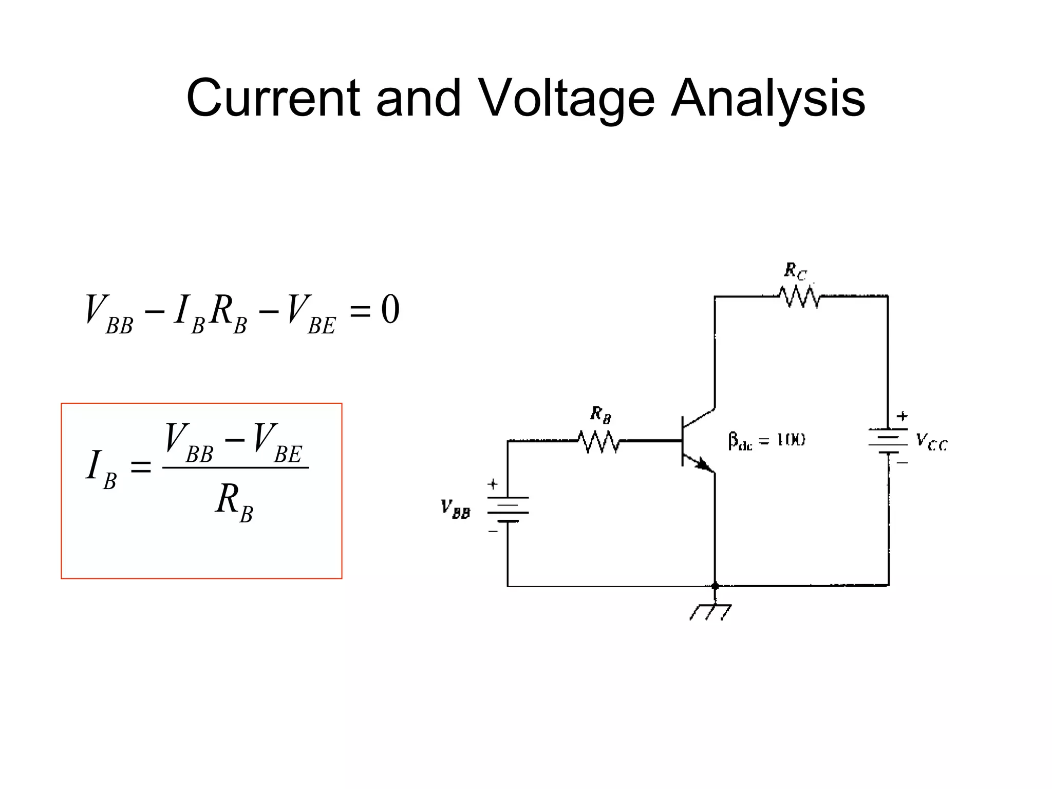
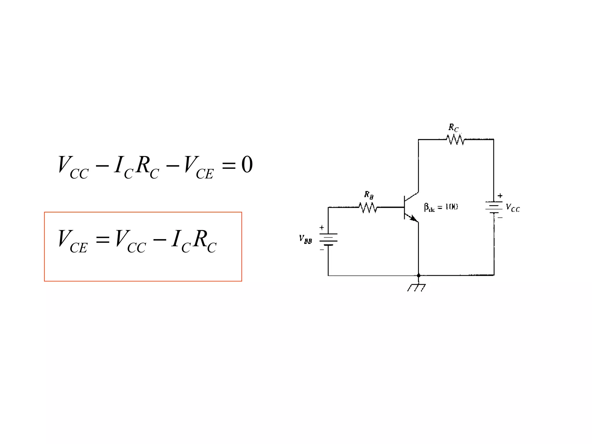
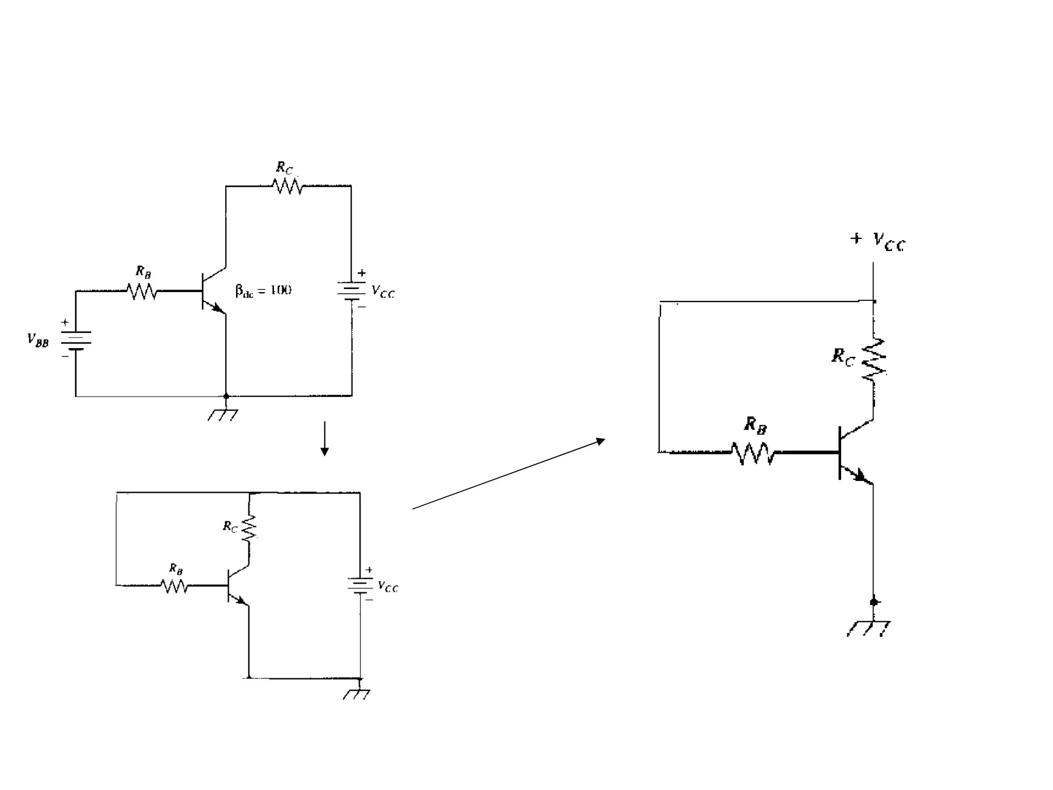
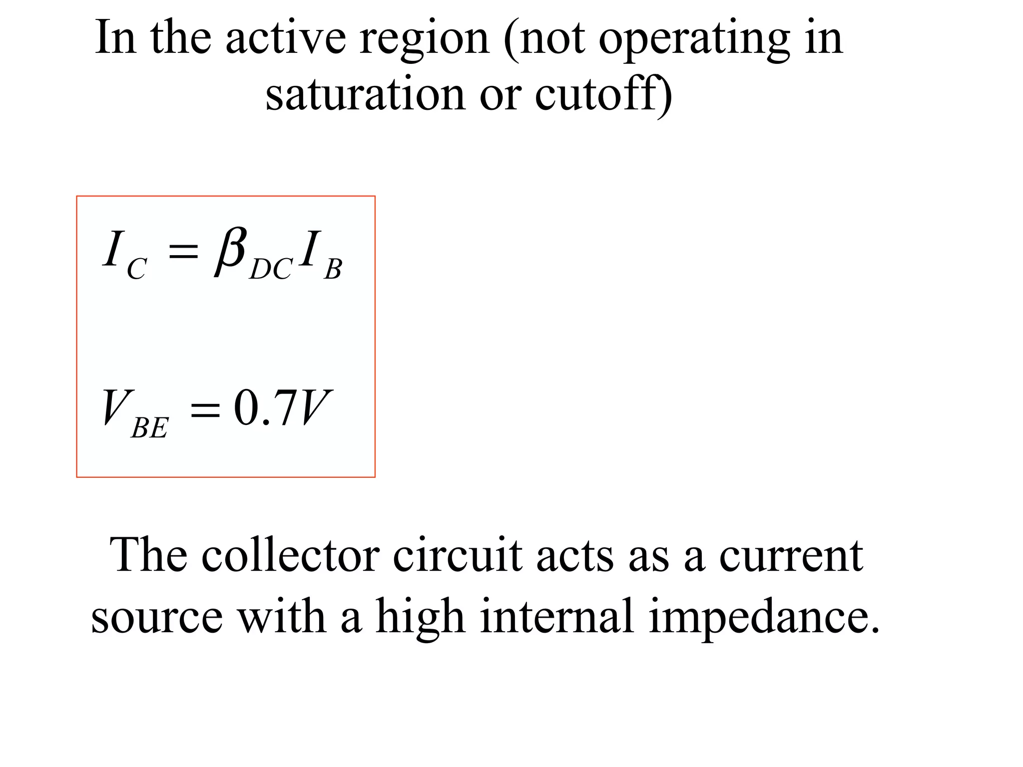
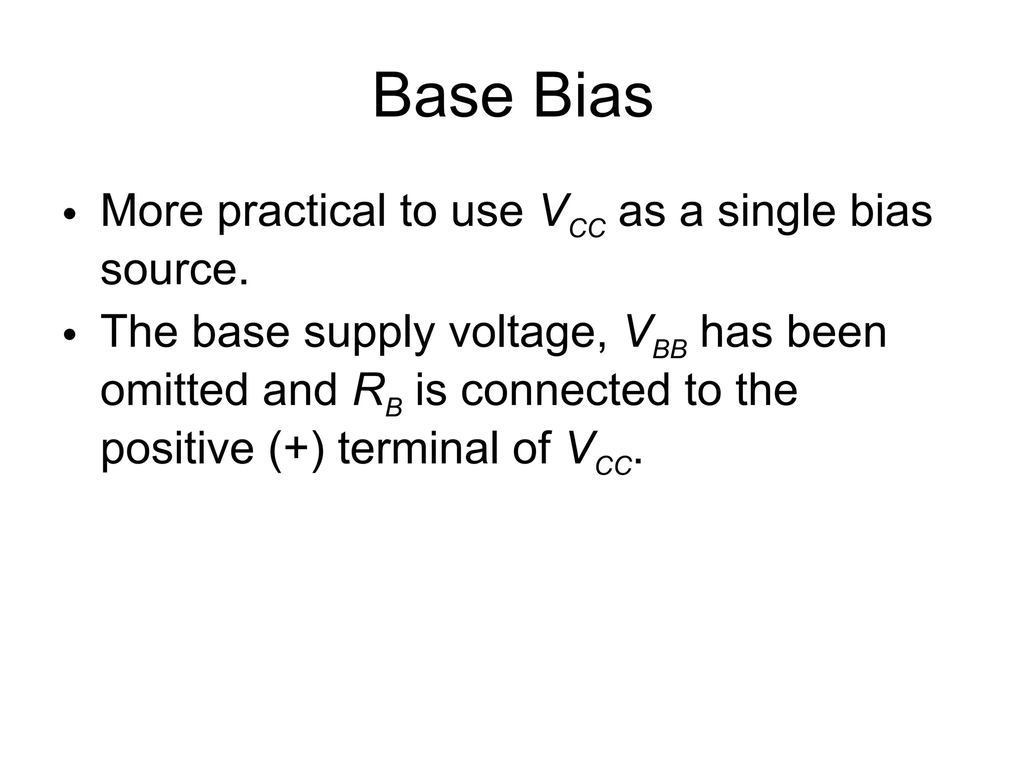
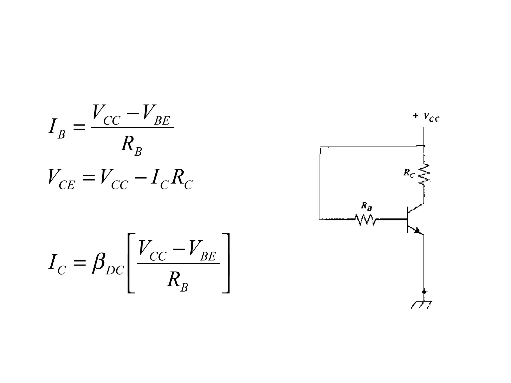
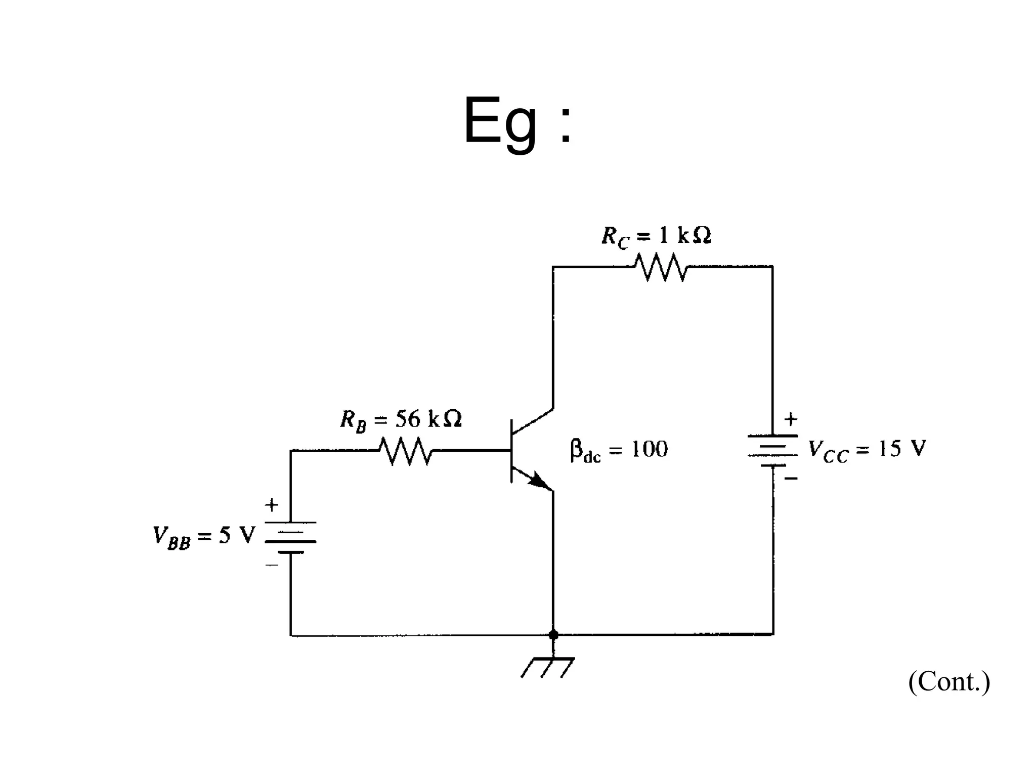
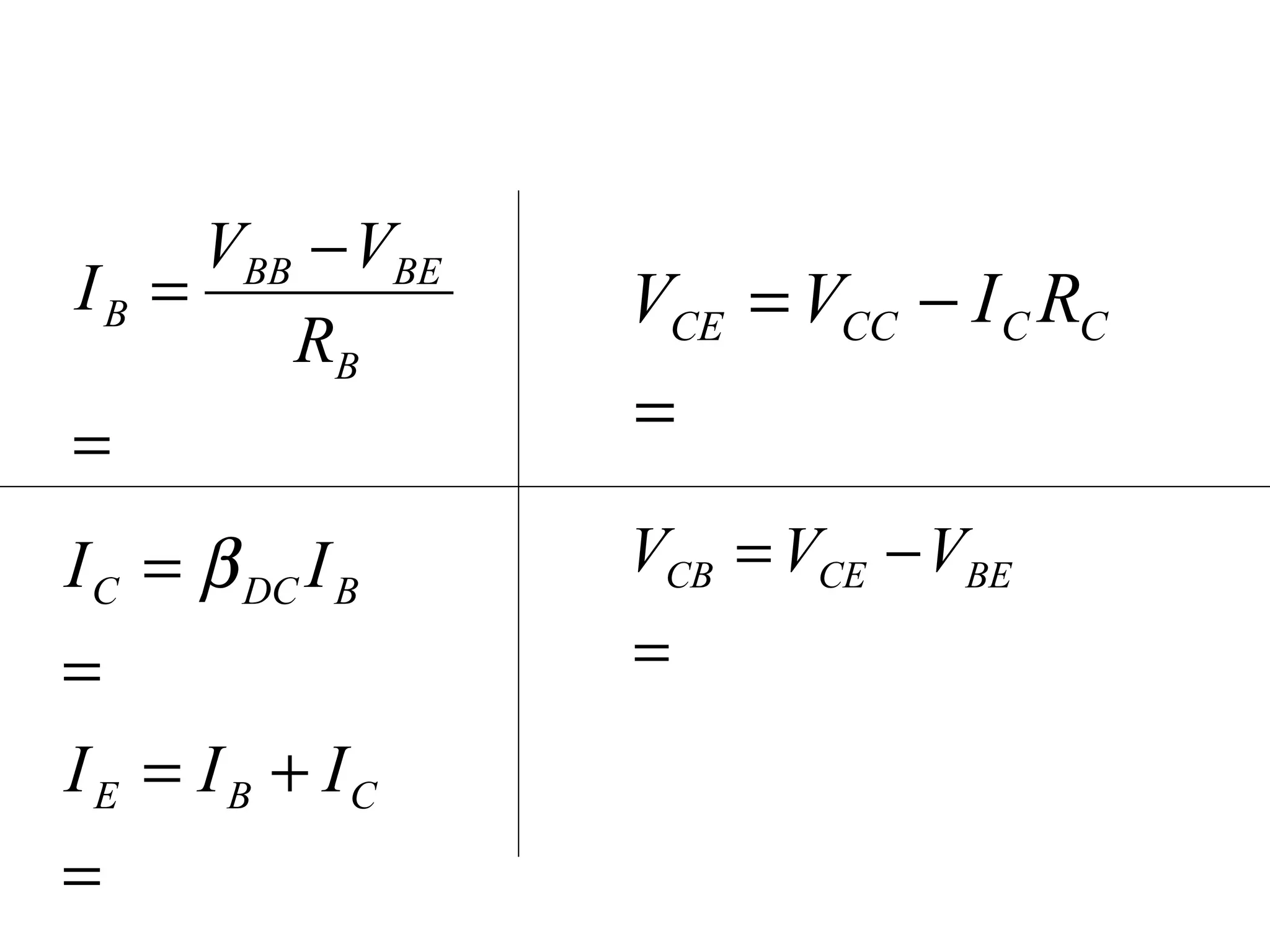
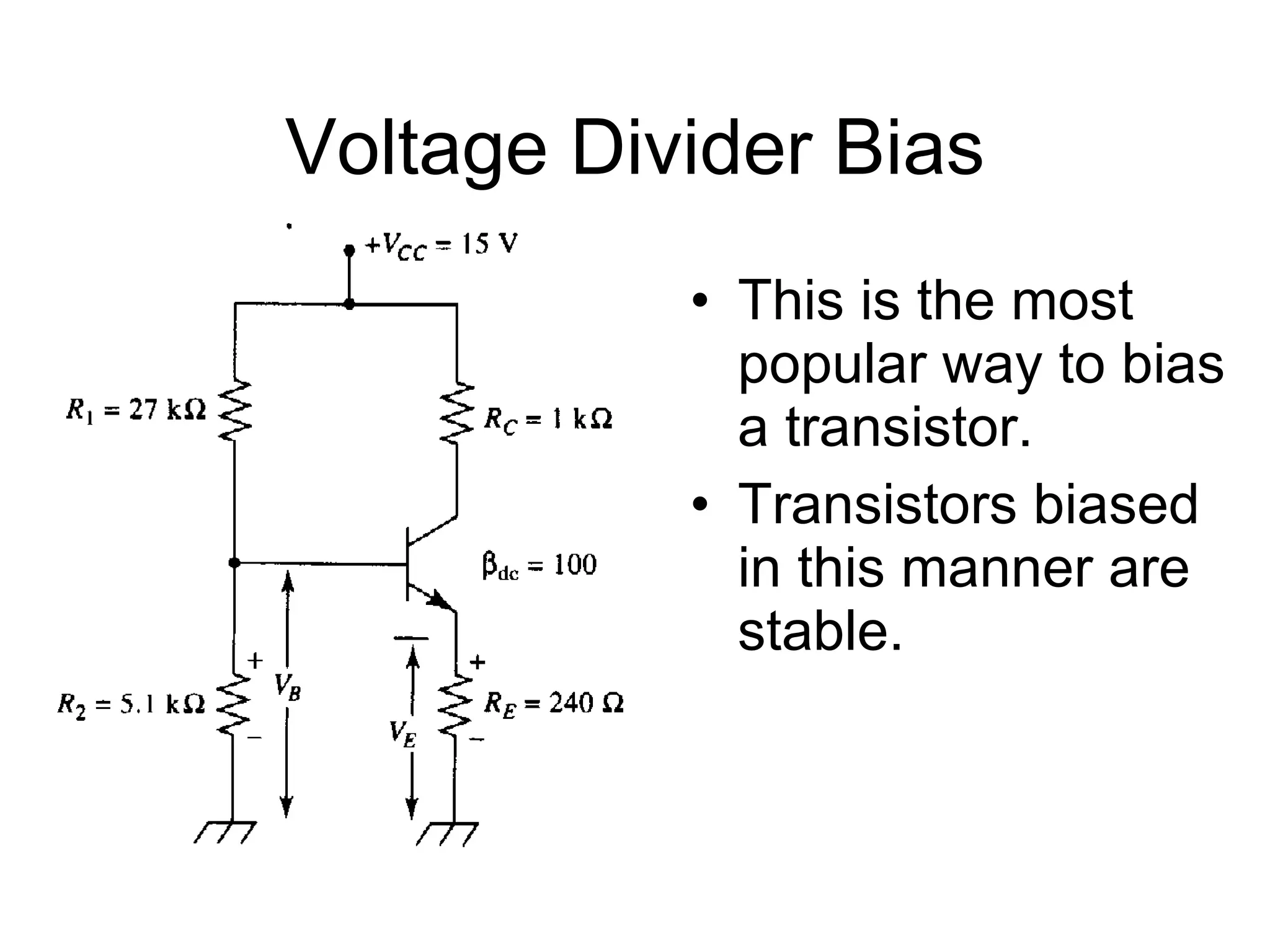
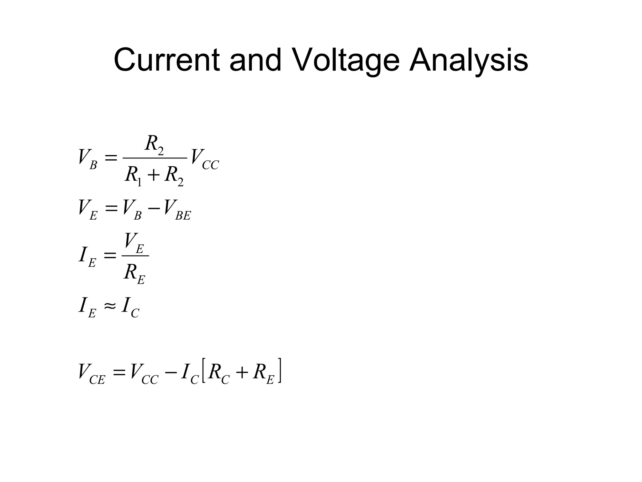
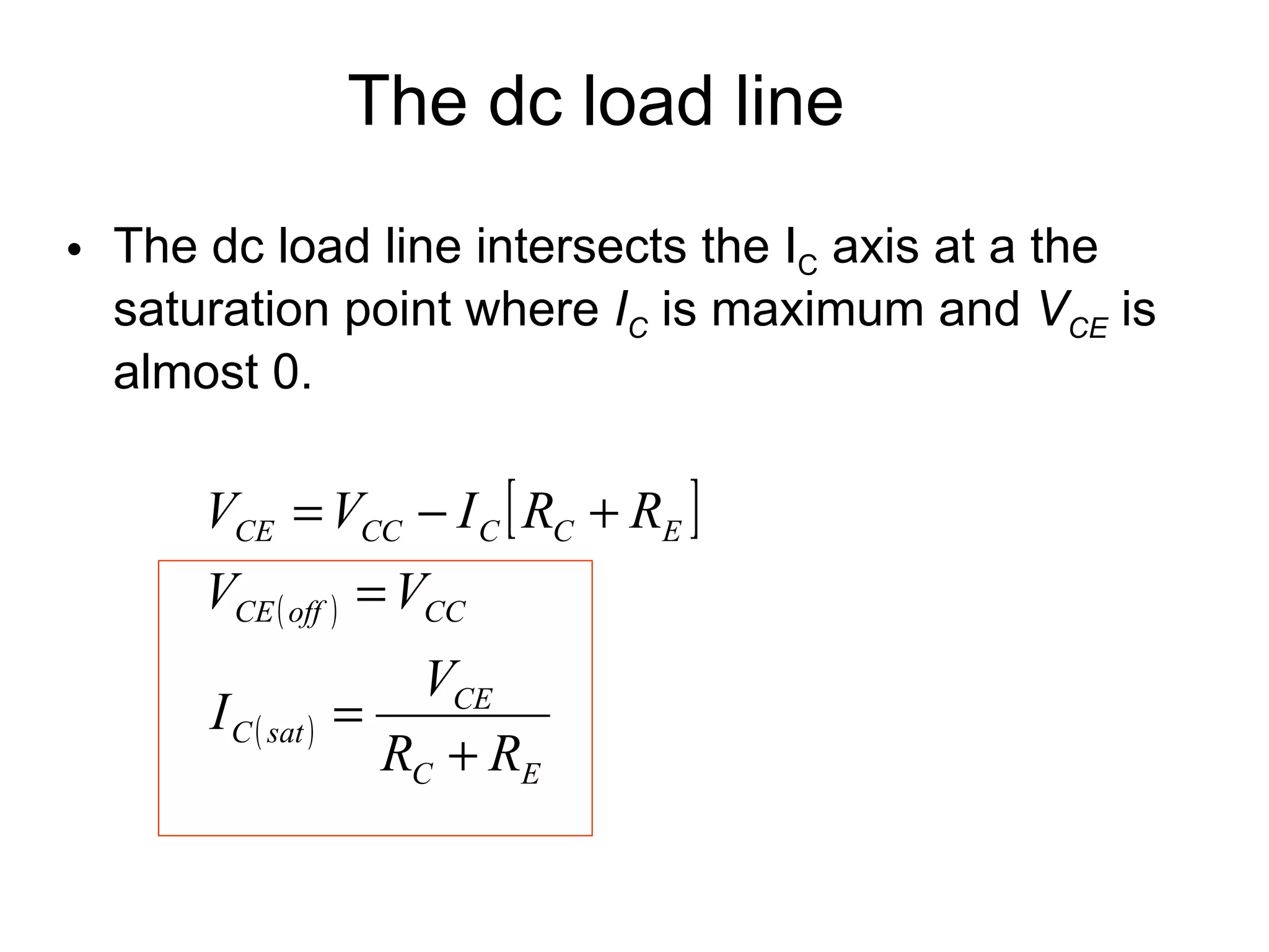
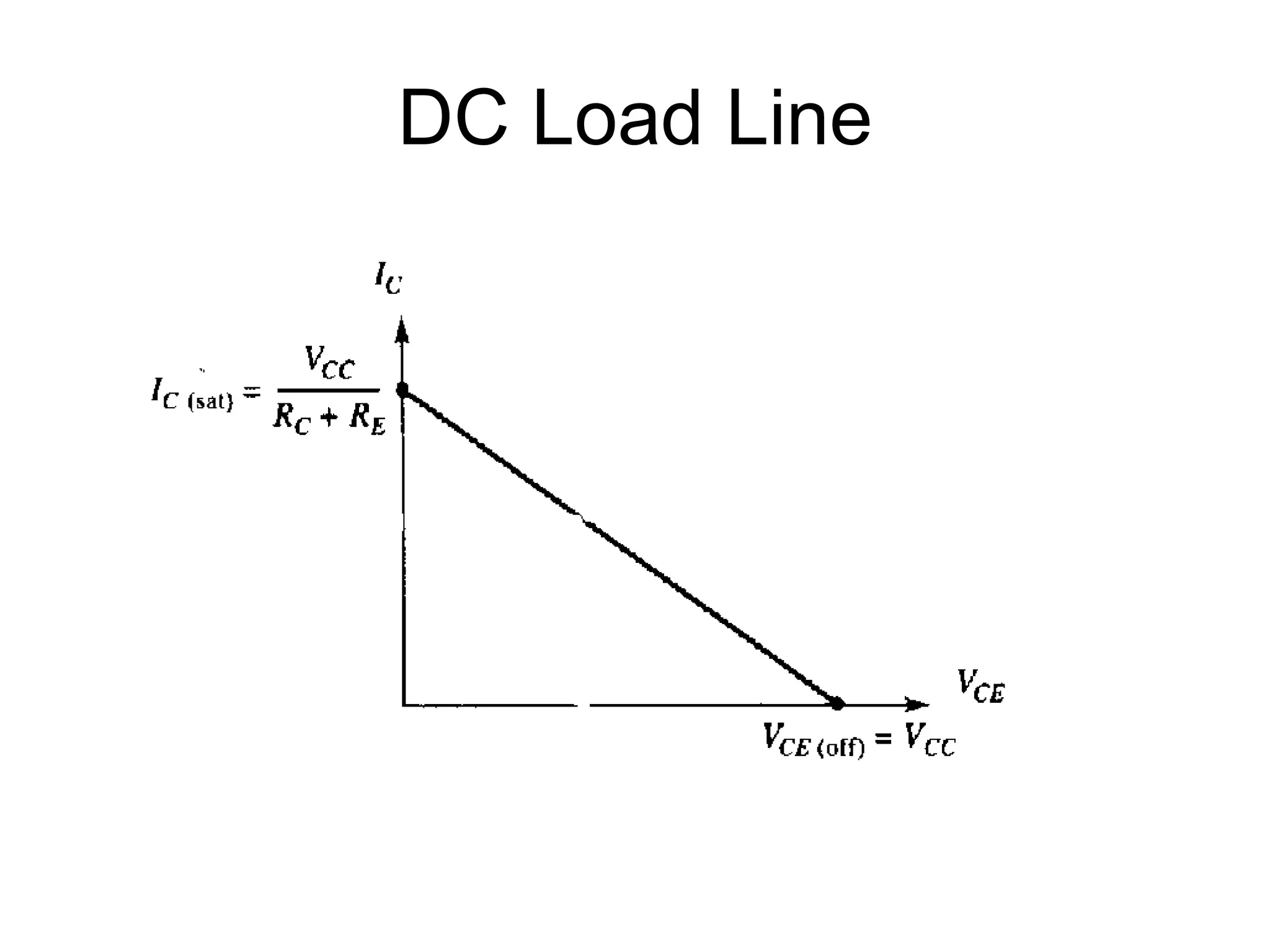
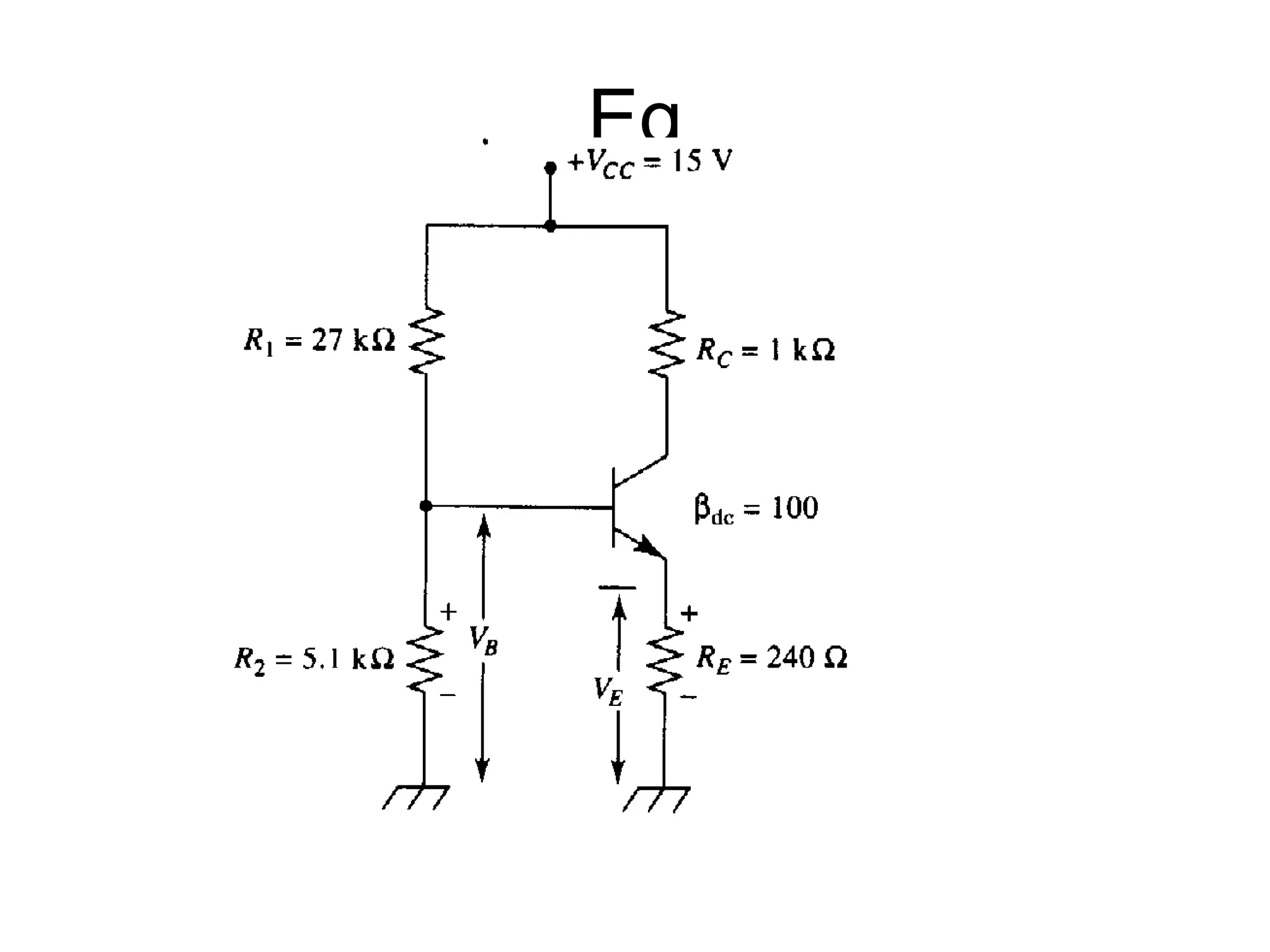
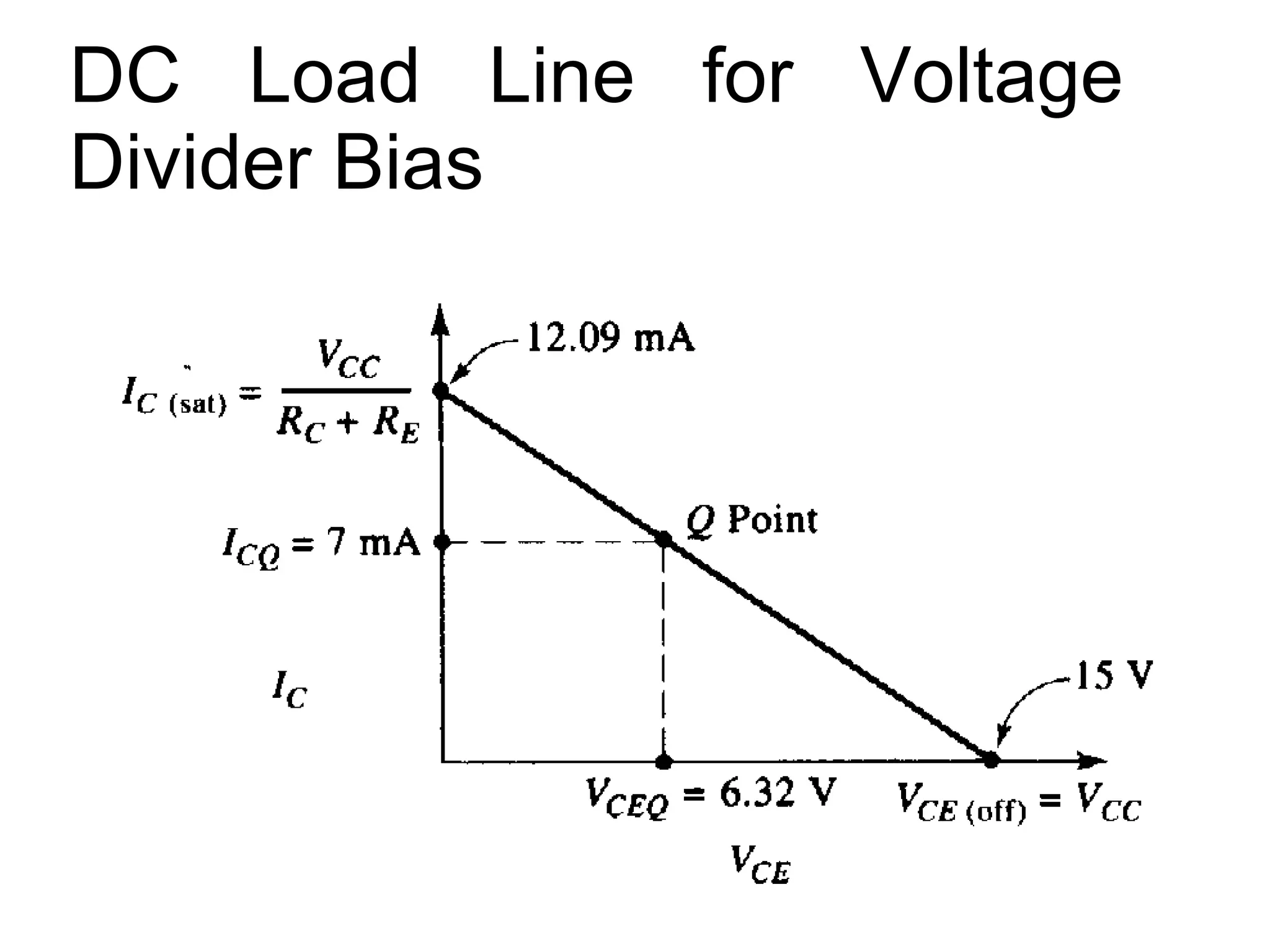
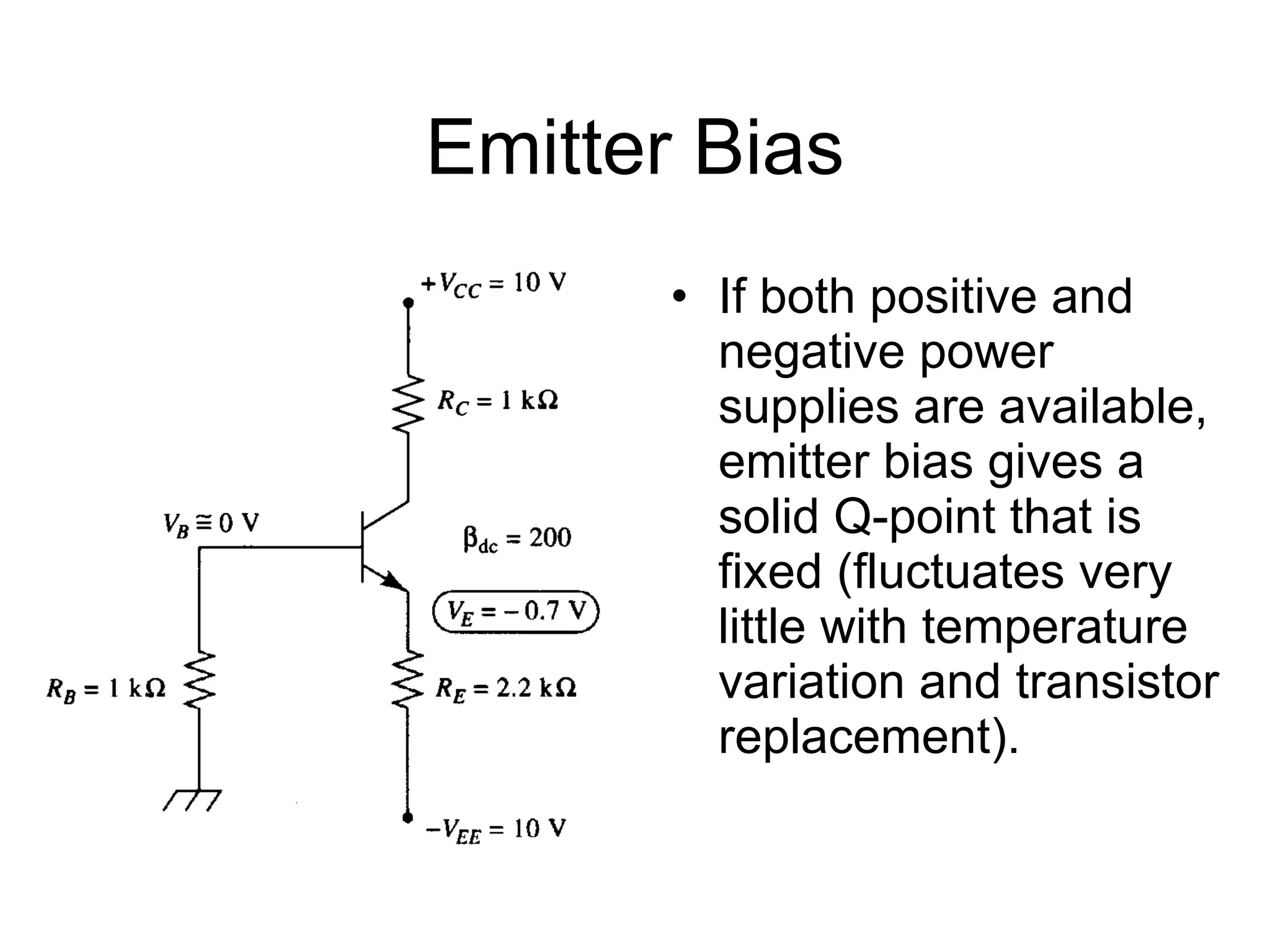
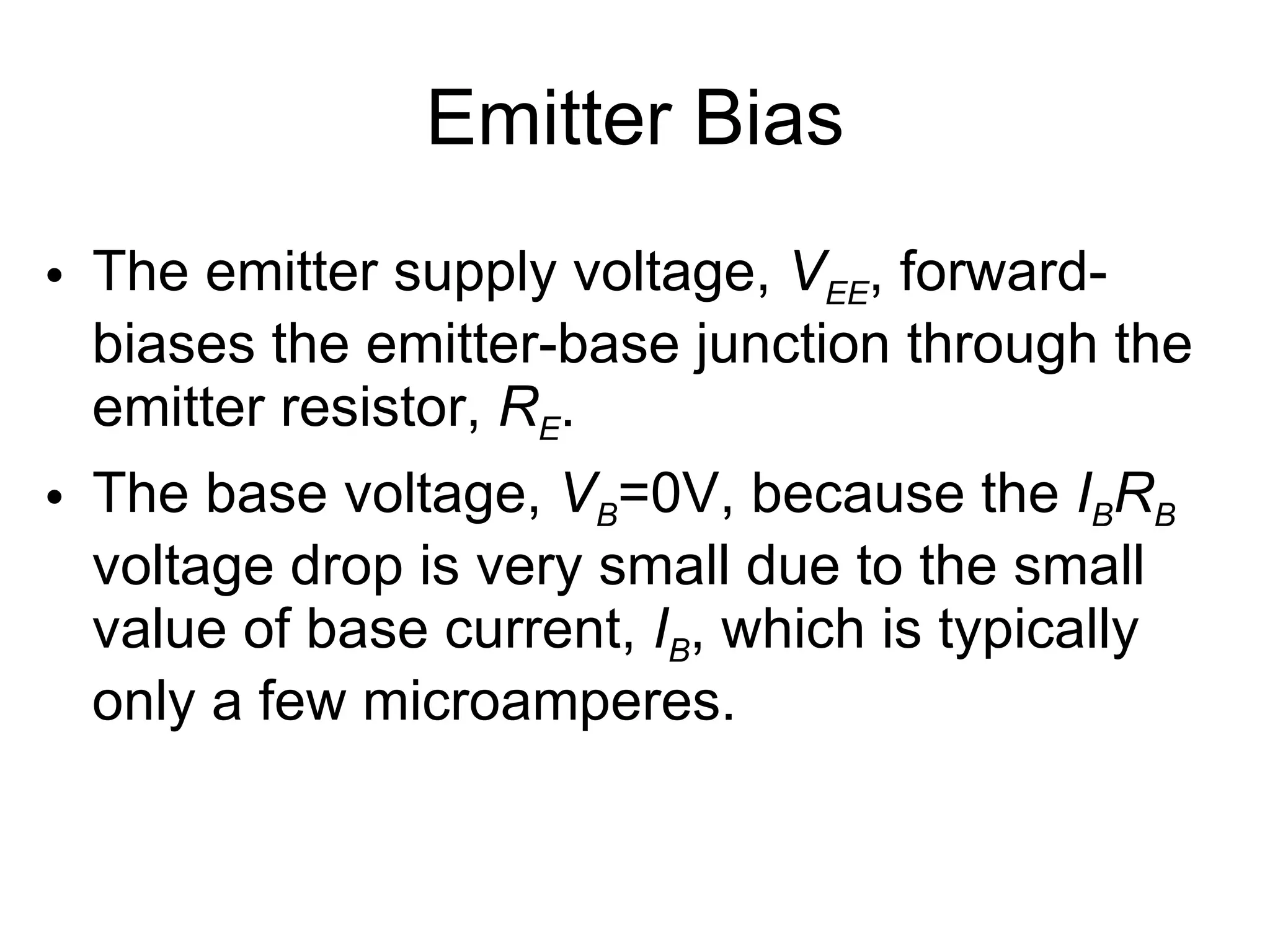
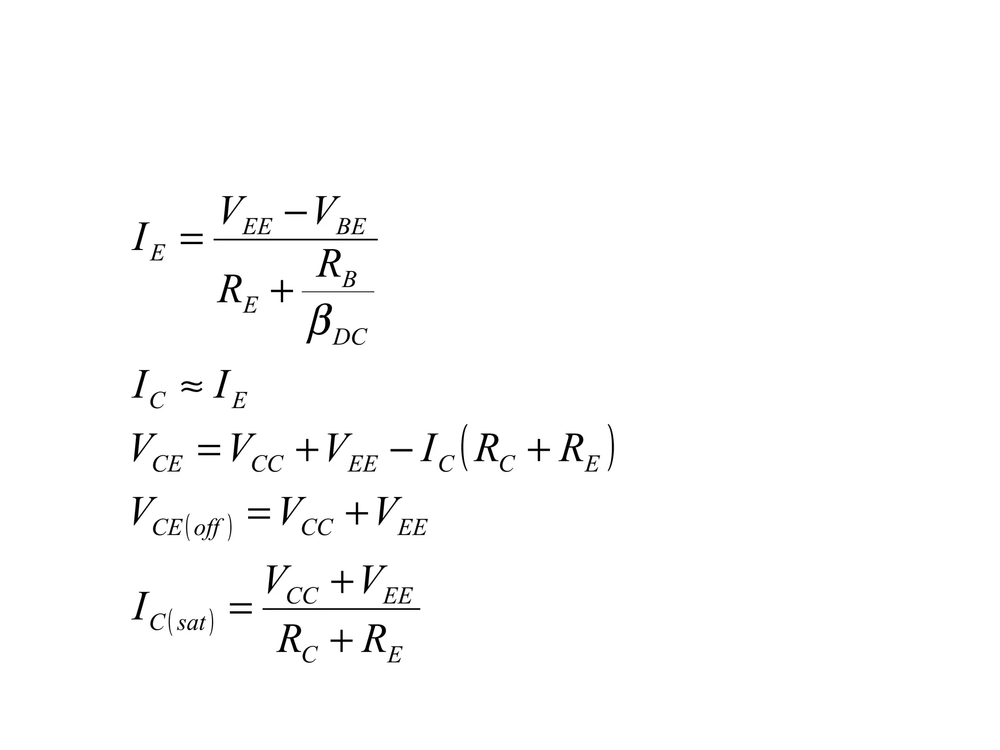
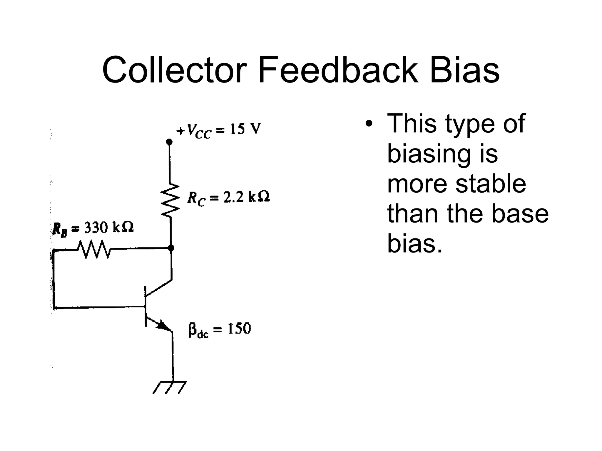
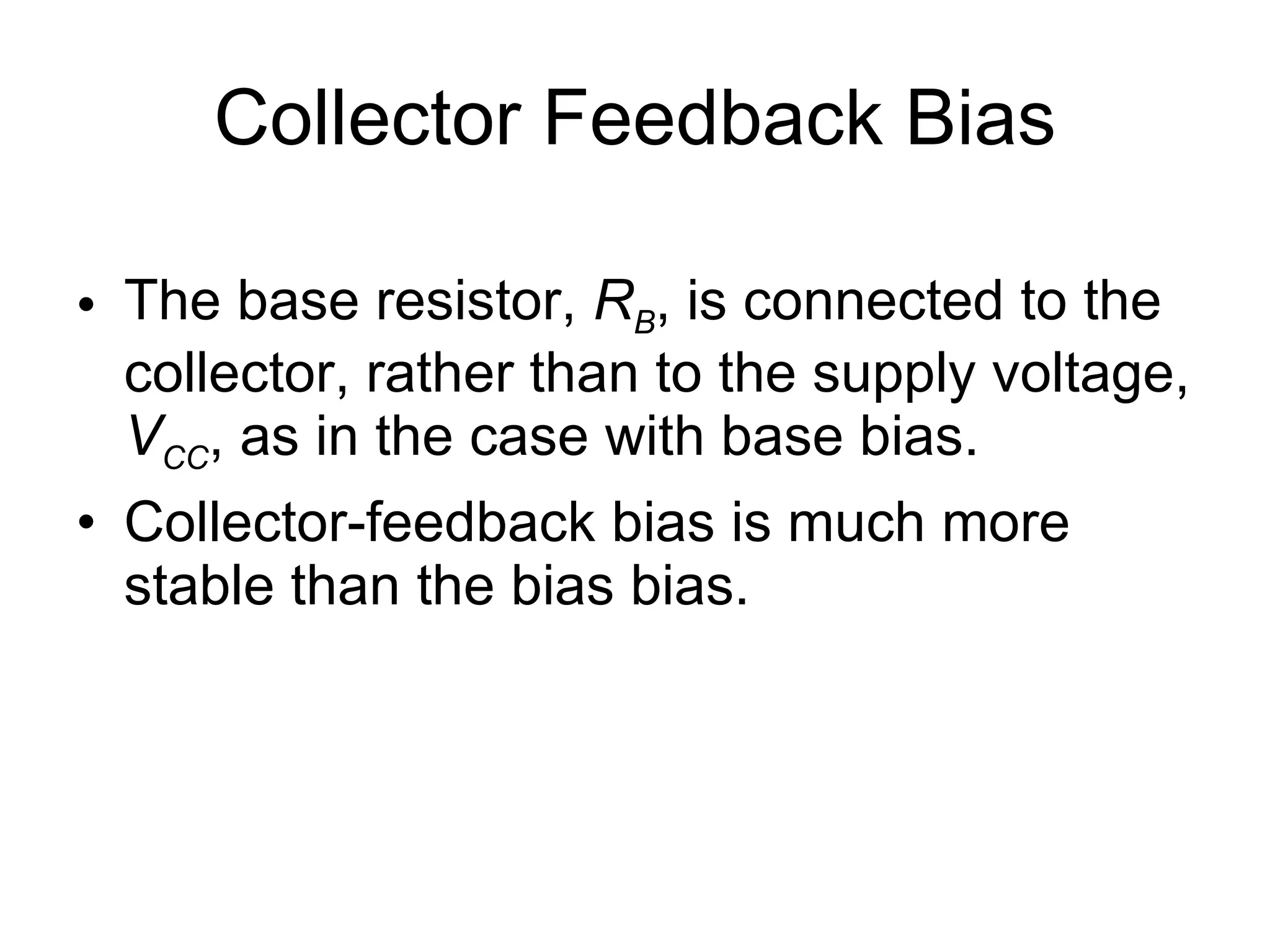
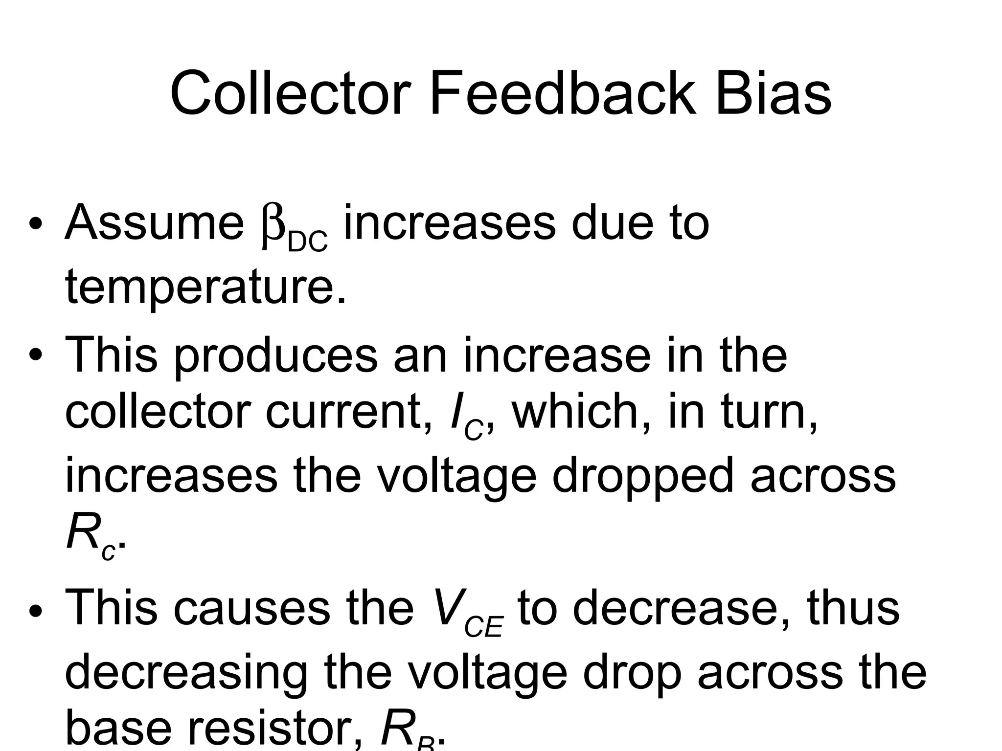
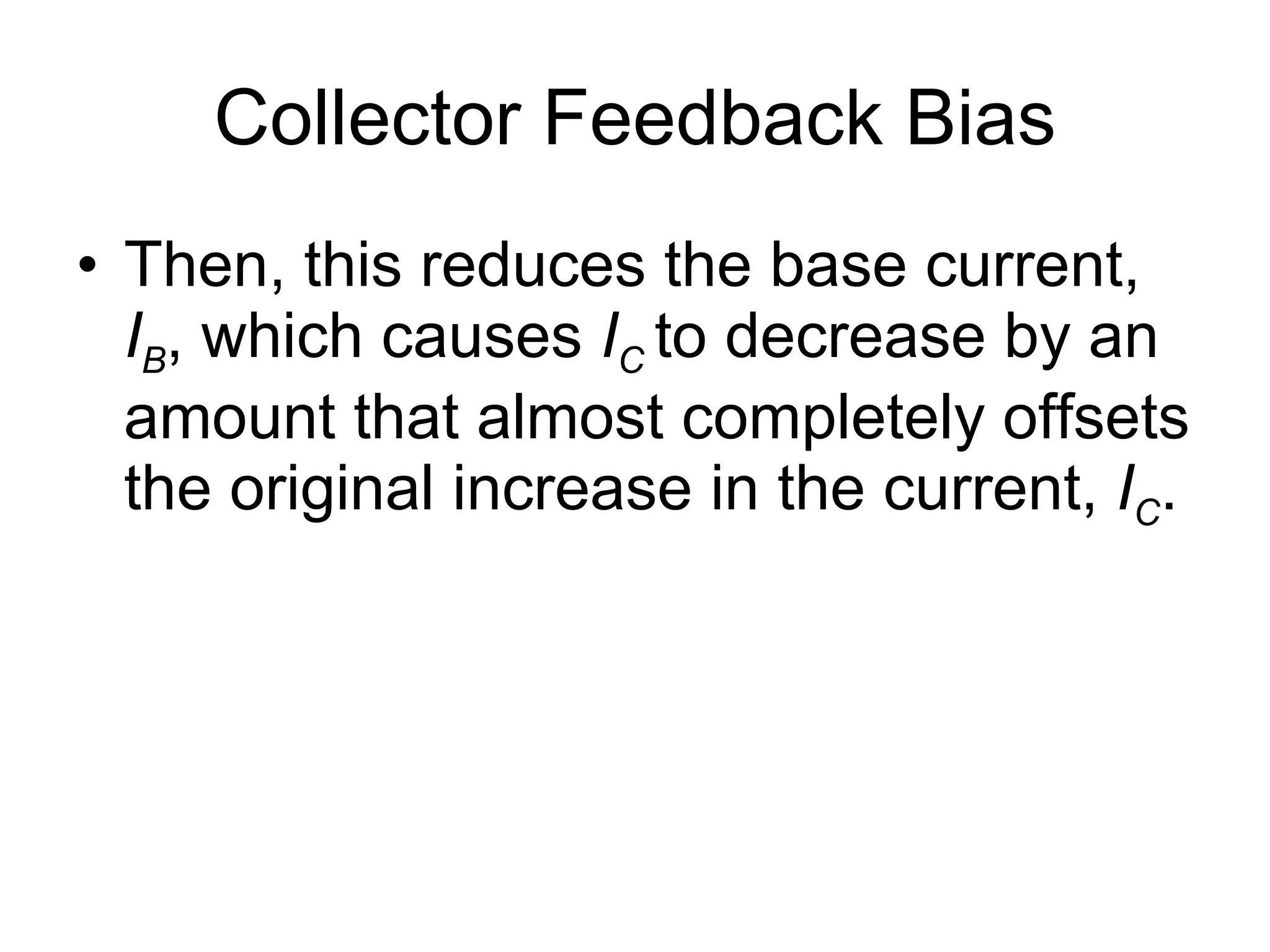
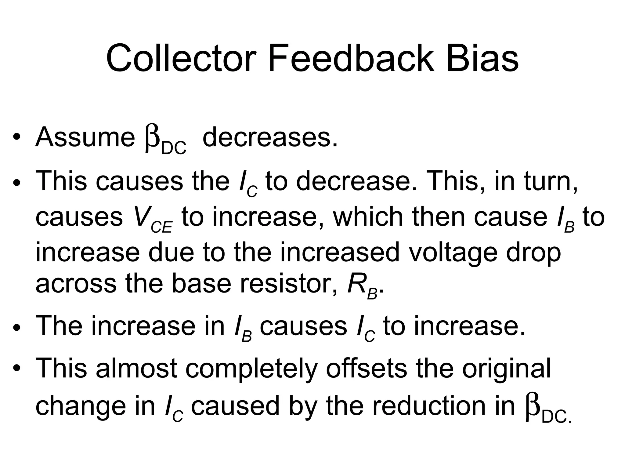
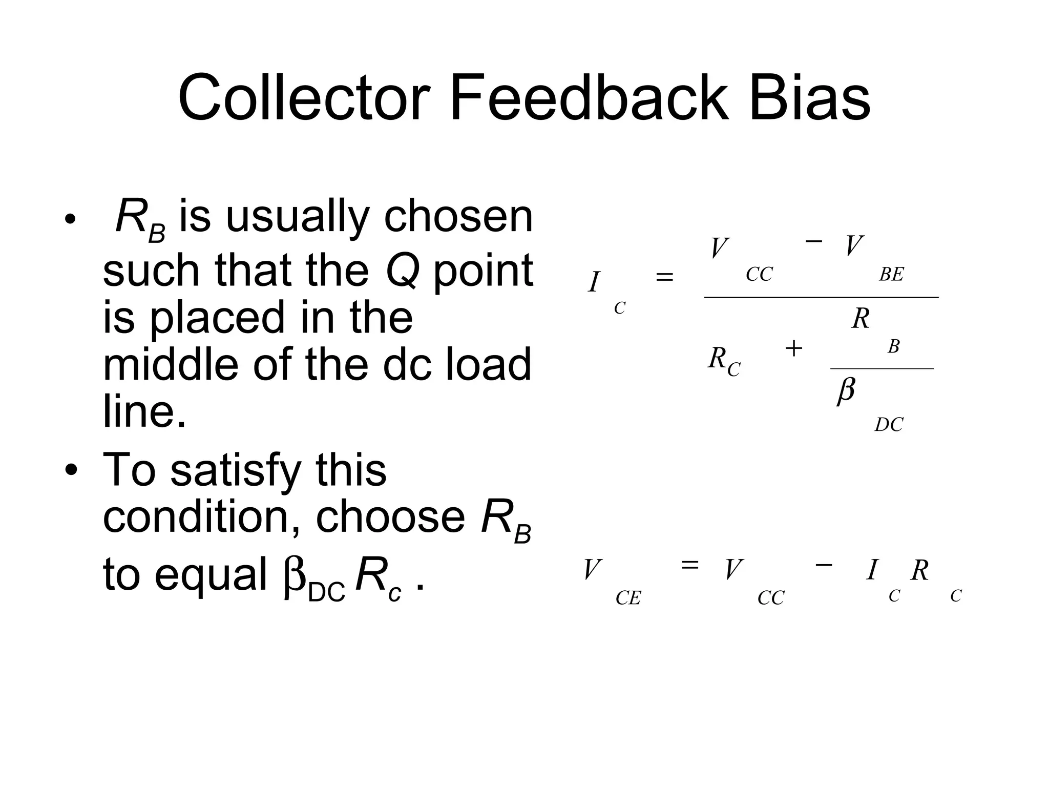
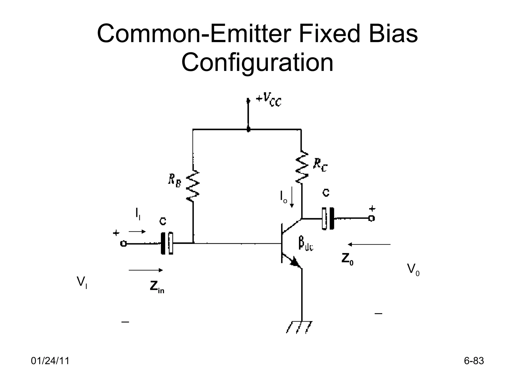
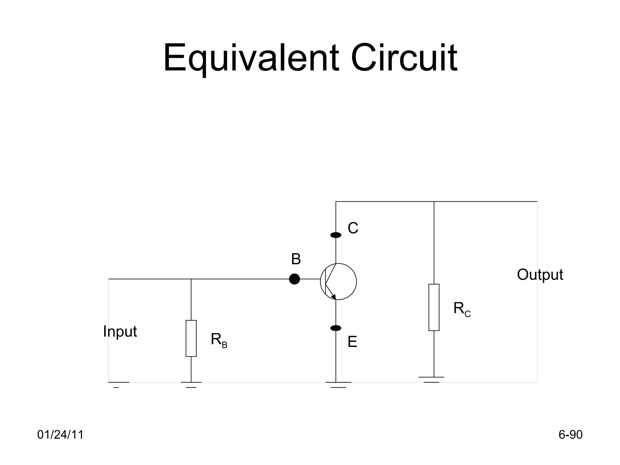
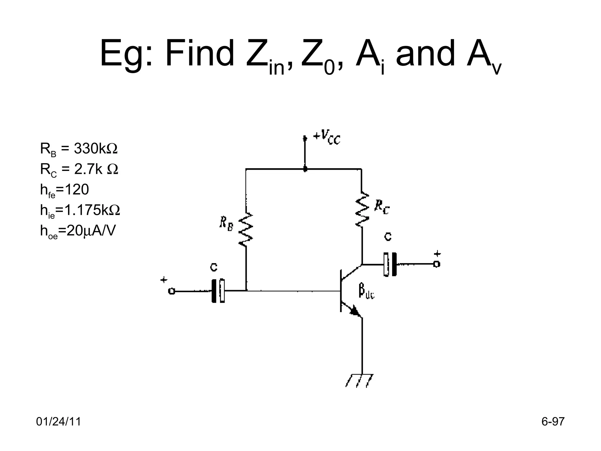
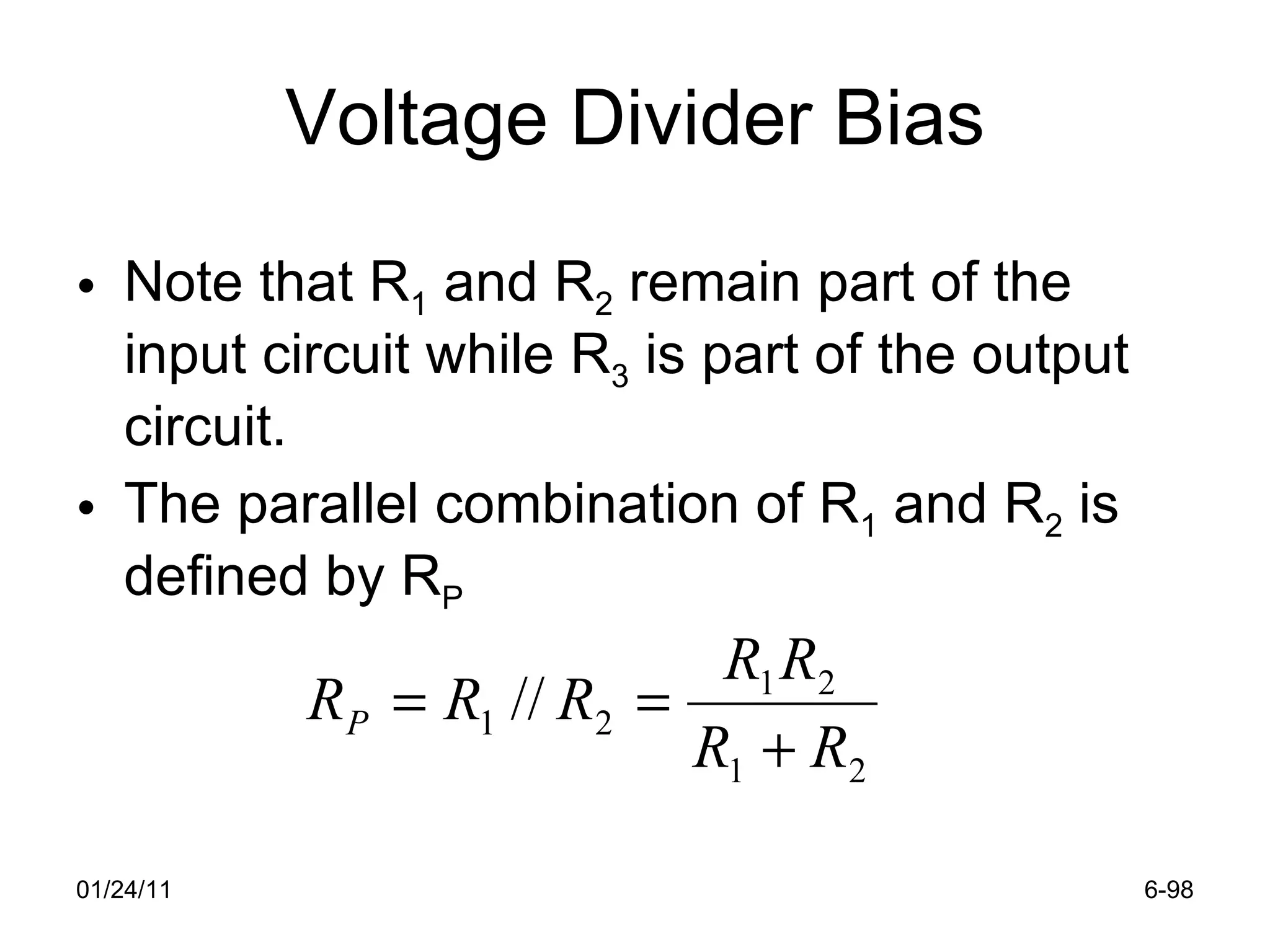
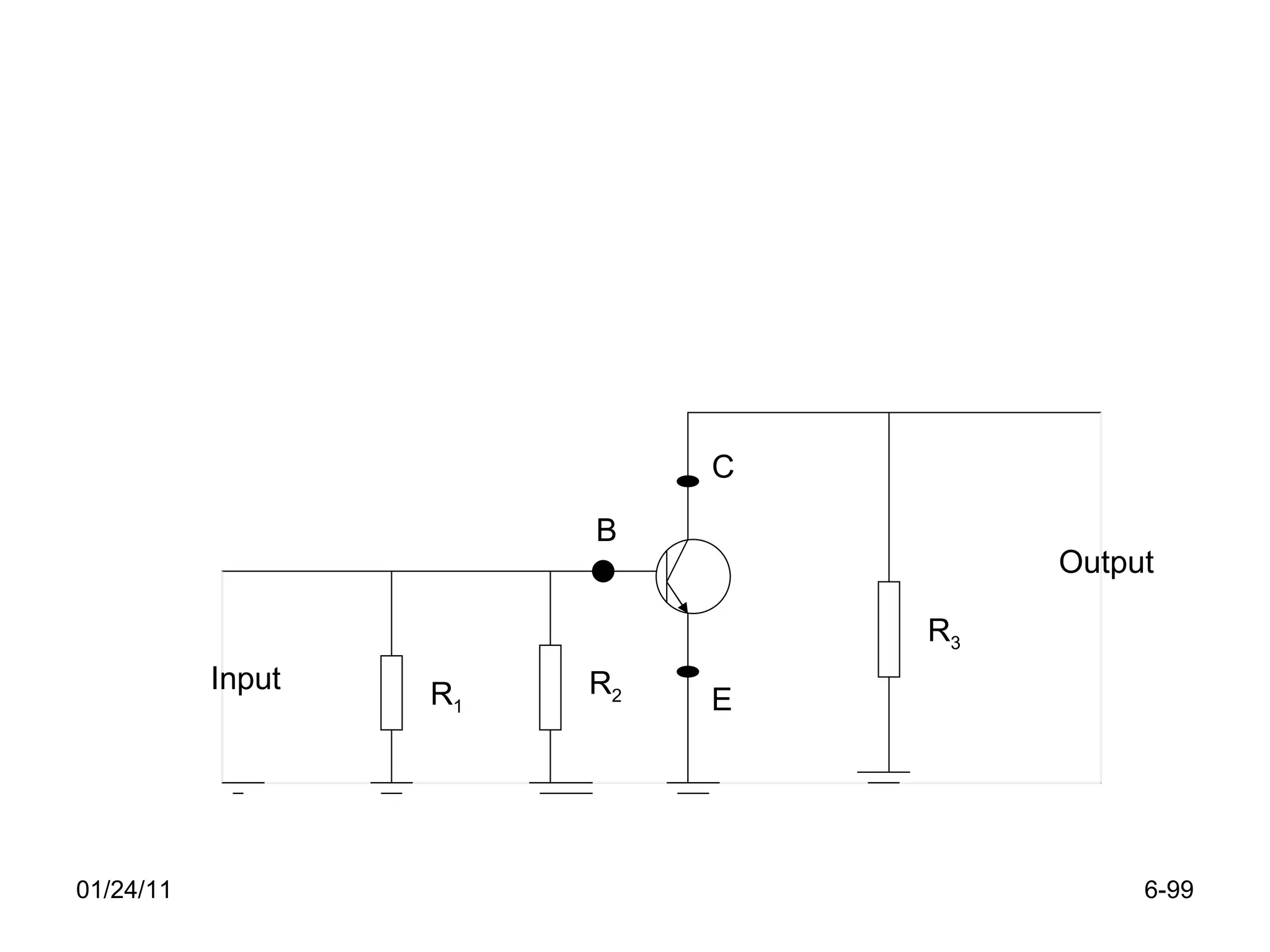
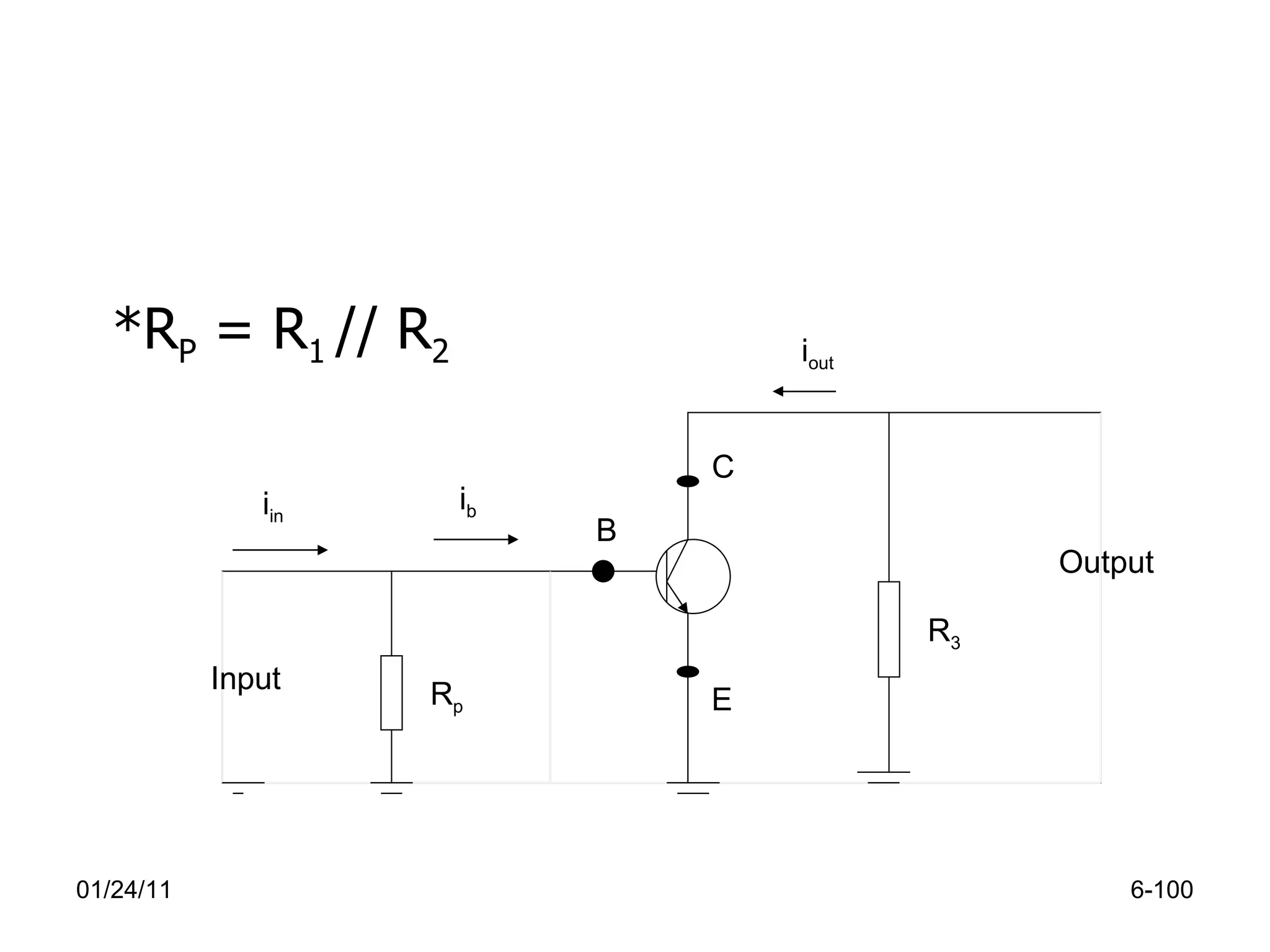
- BJT biasing configurations like base, emitter, voltage divider, and collector feedback bias.
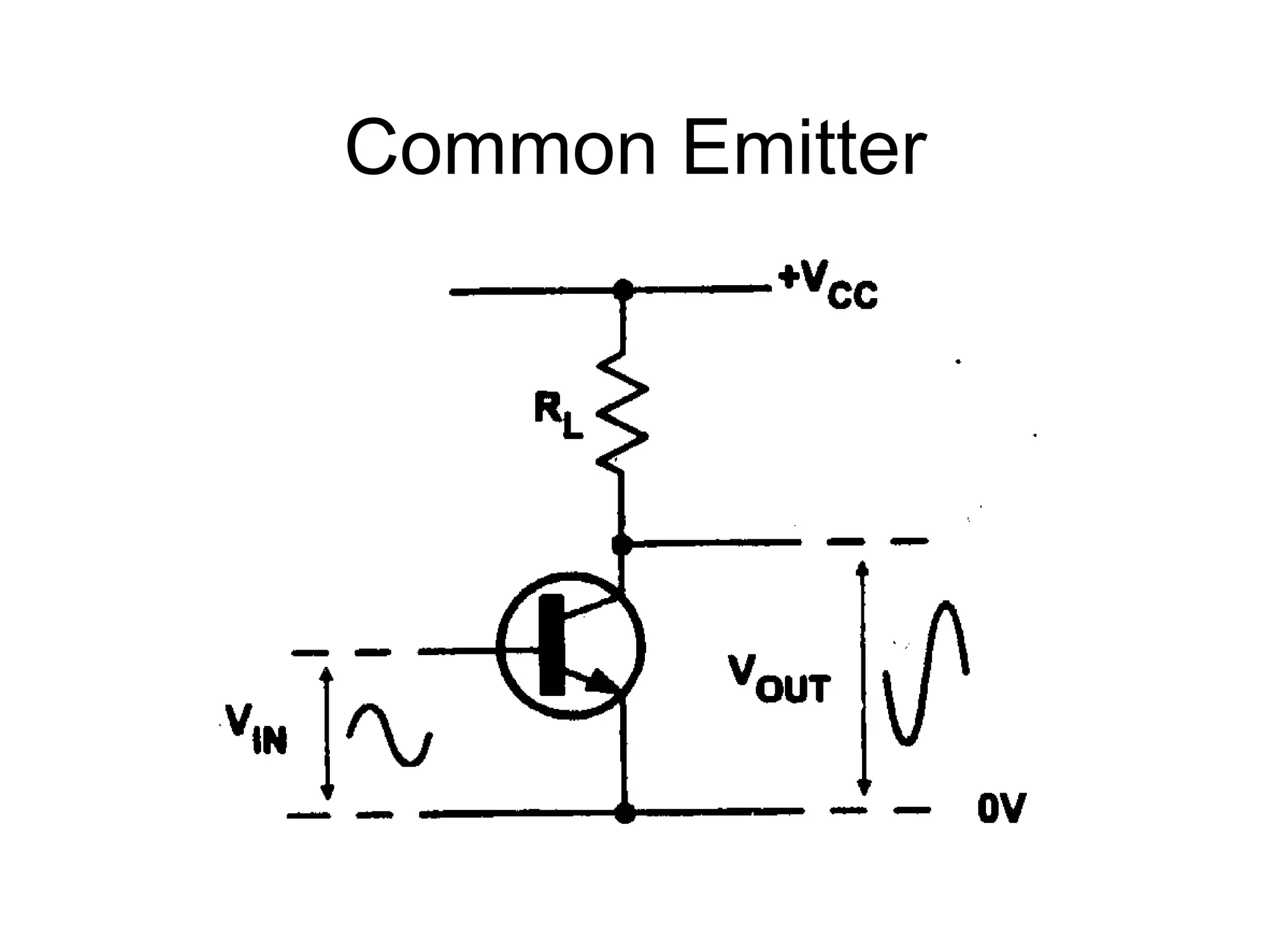
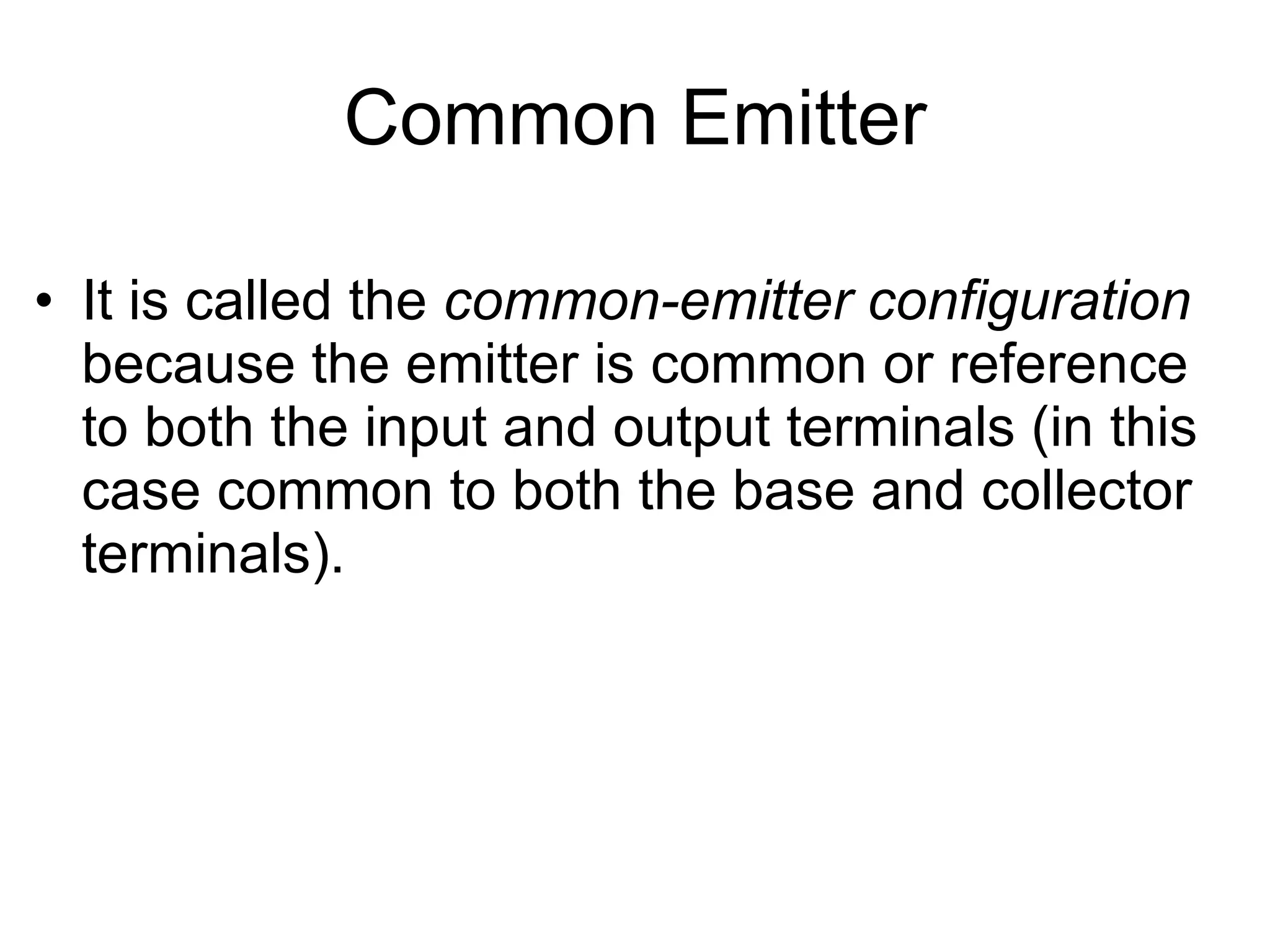
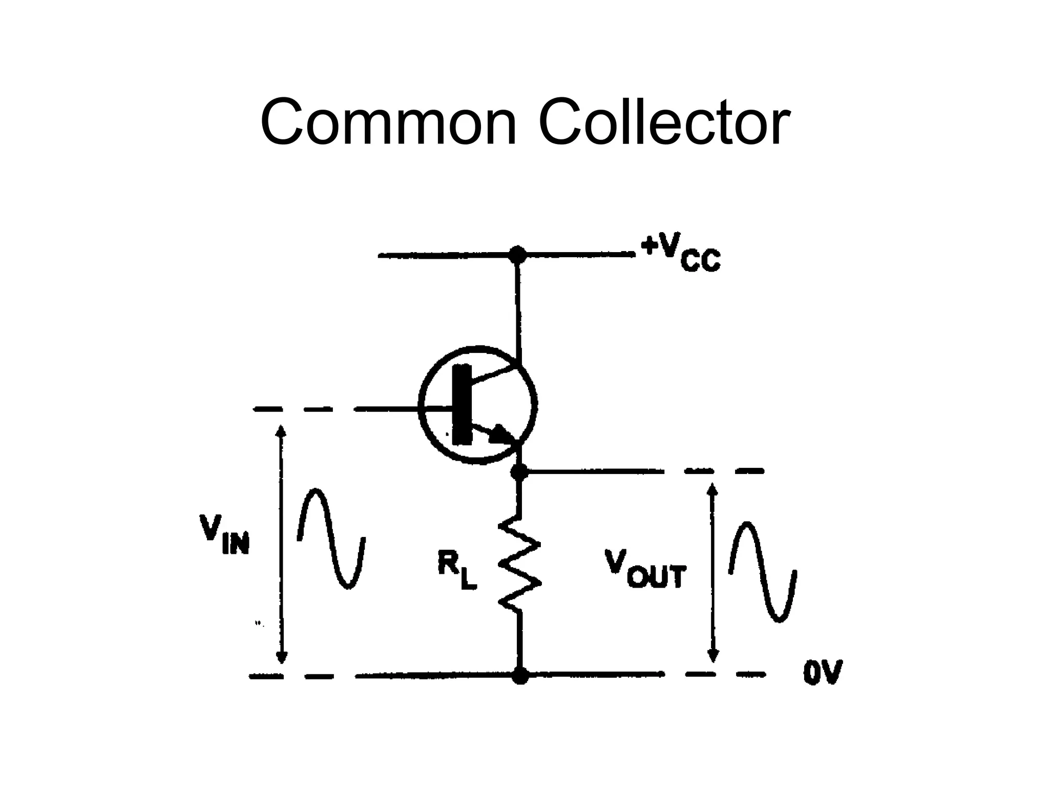
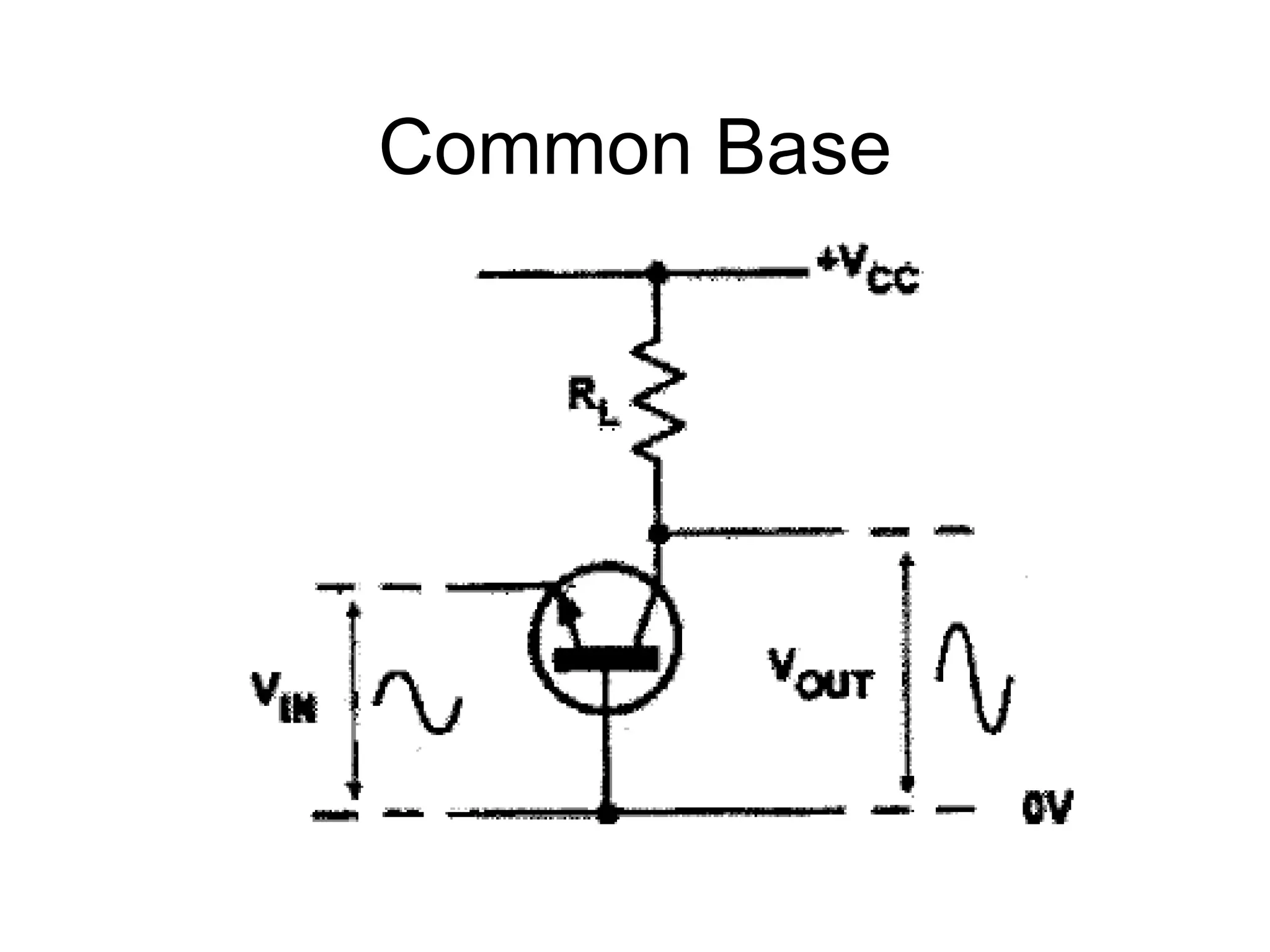
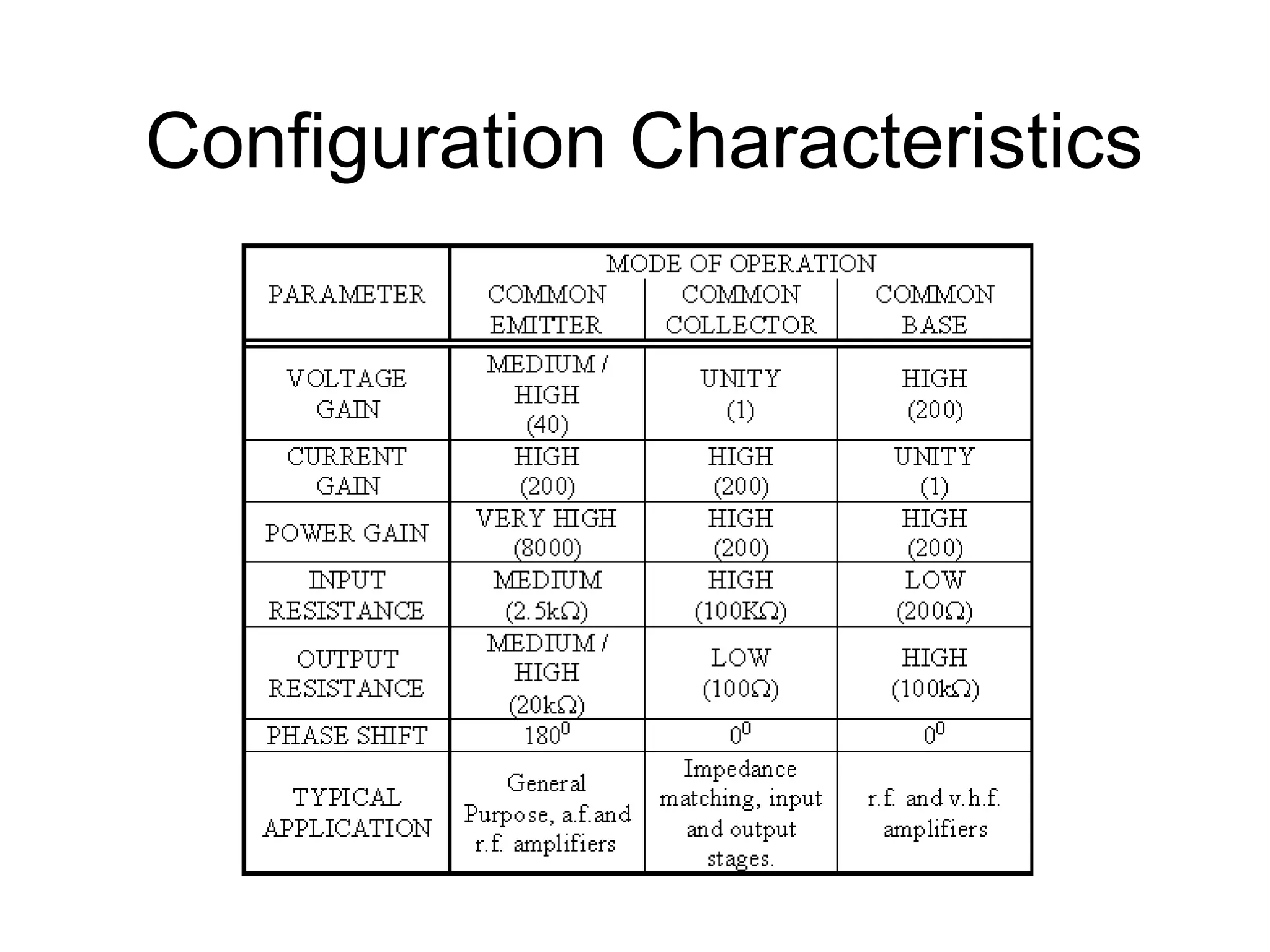
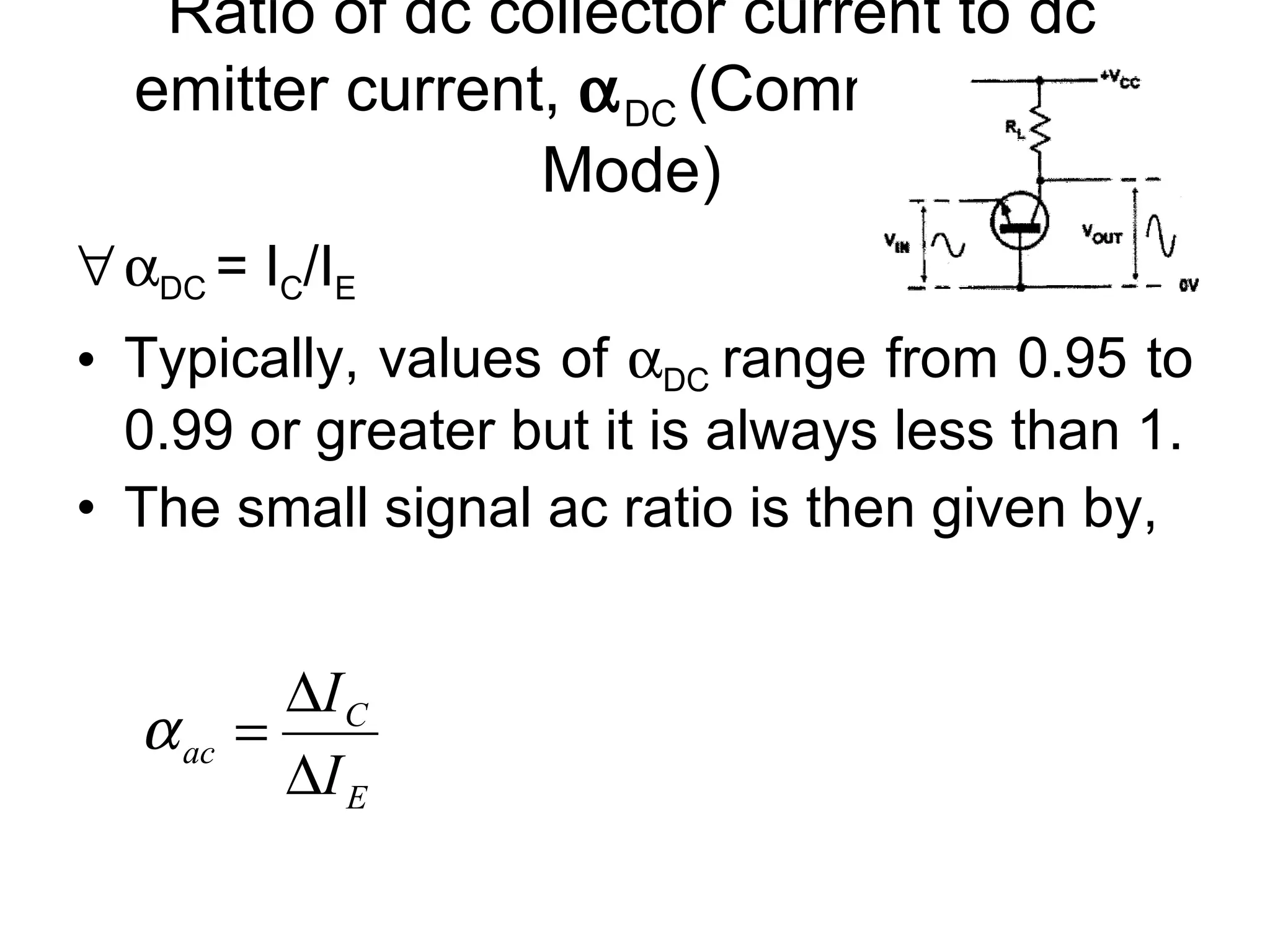
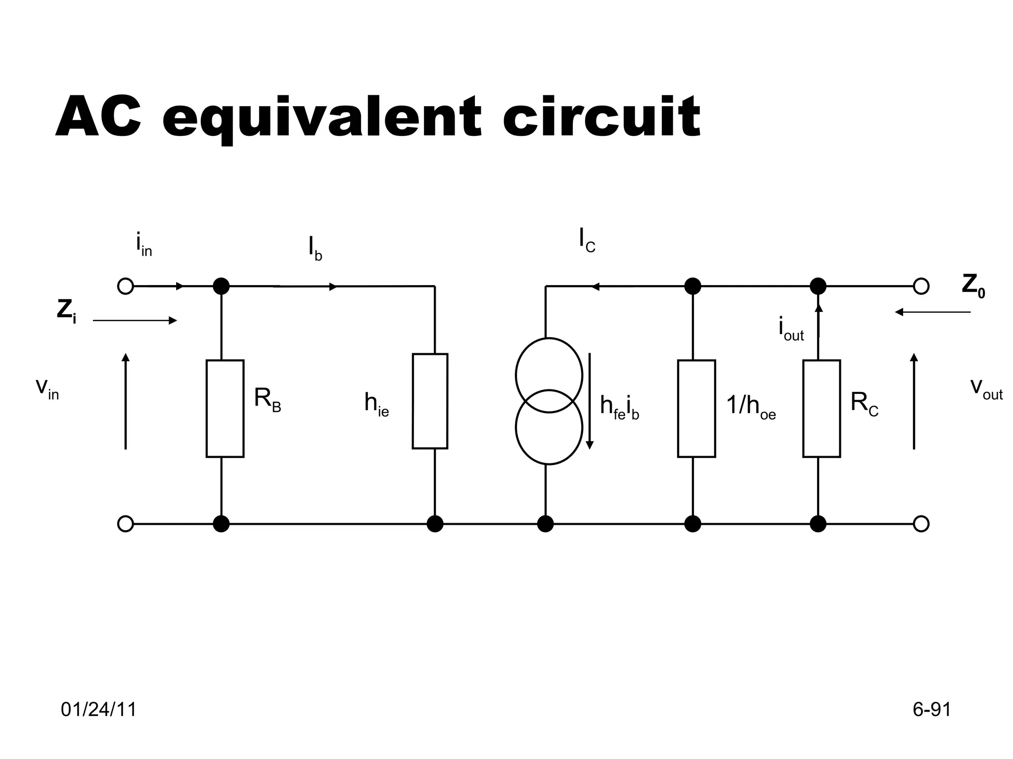
- BJT amplifier configurations including common emitter, common base, and common collector.
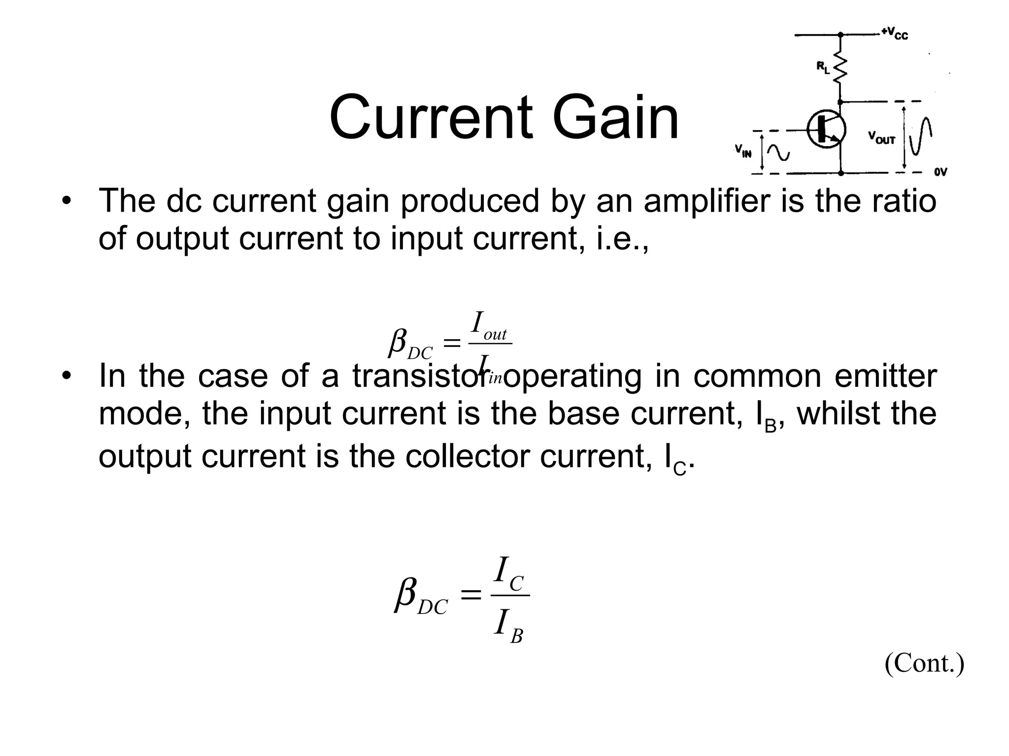
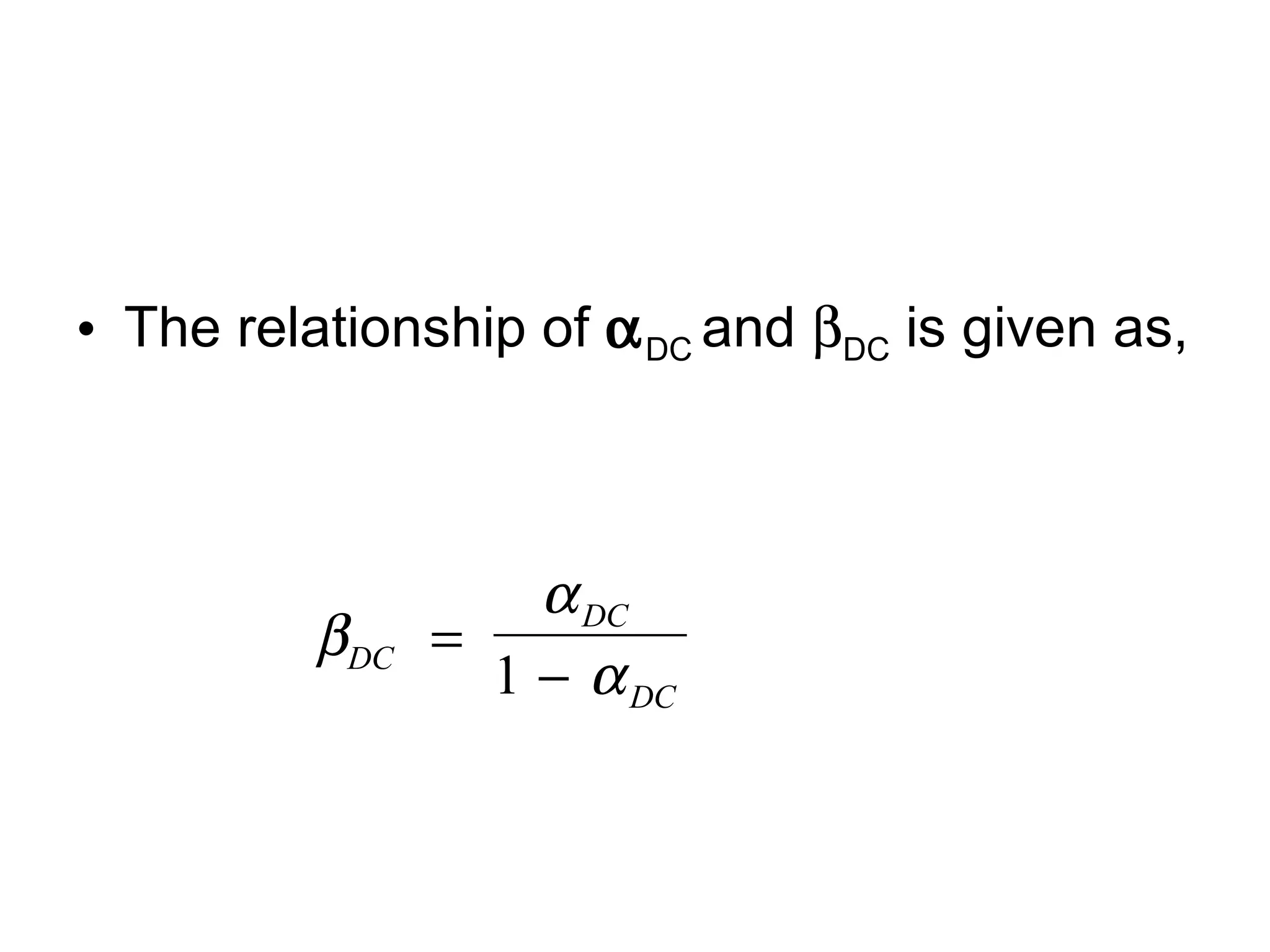
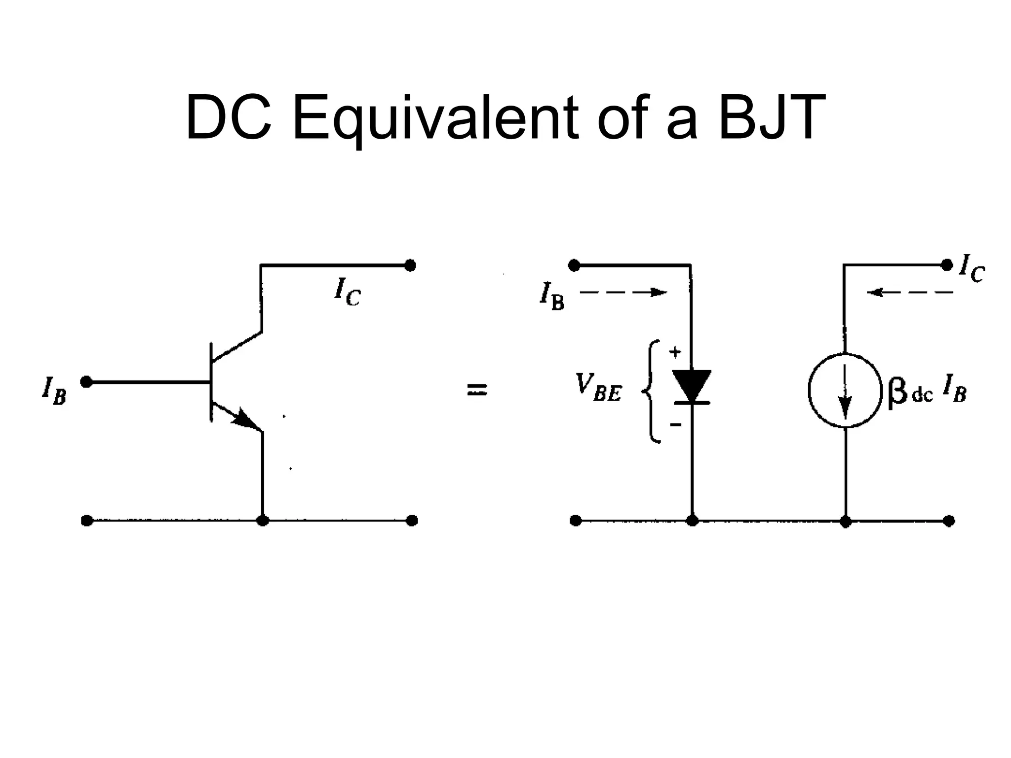
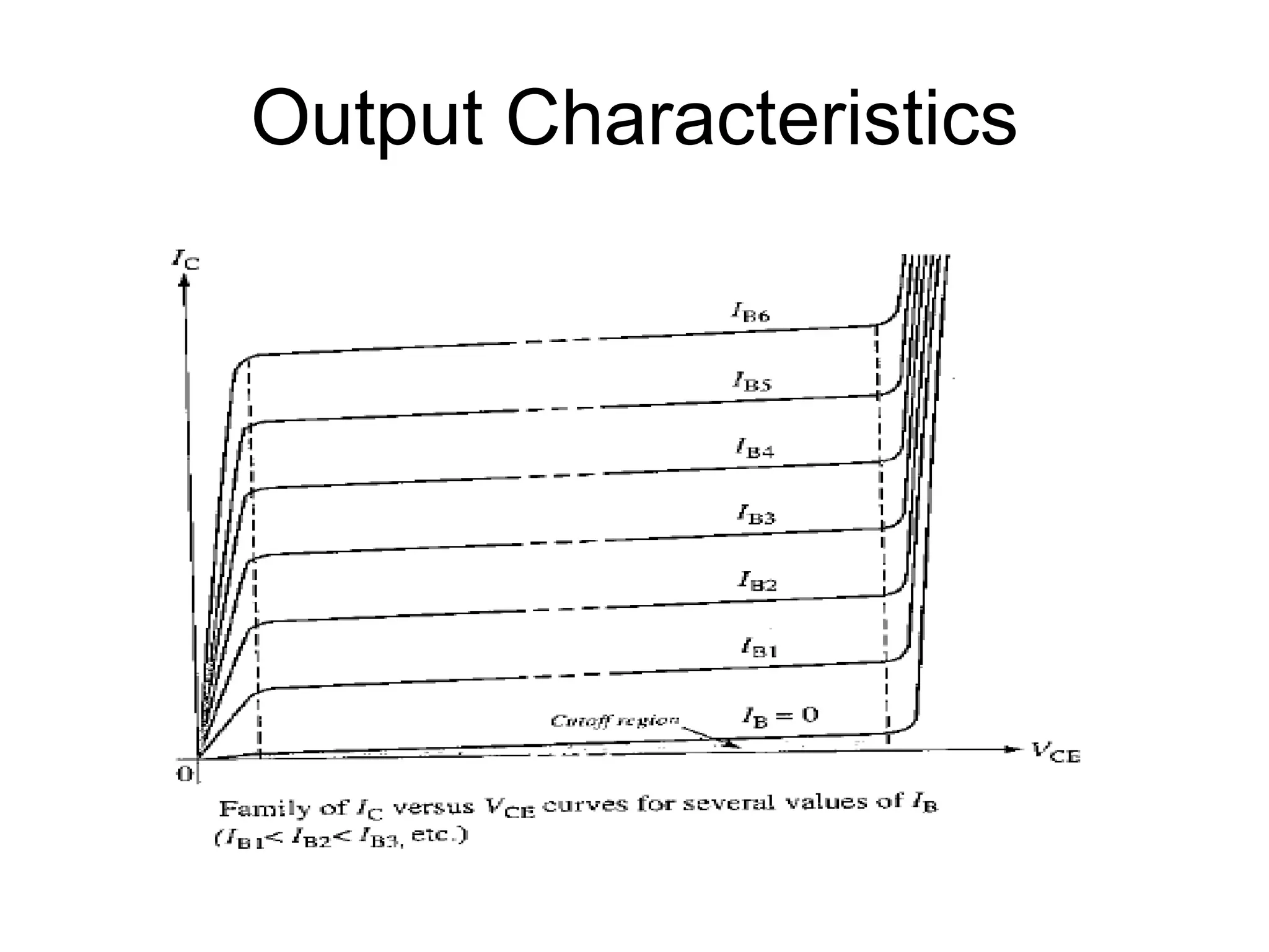
- Transistor parameters like current gain and their effects on circuit operation.
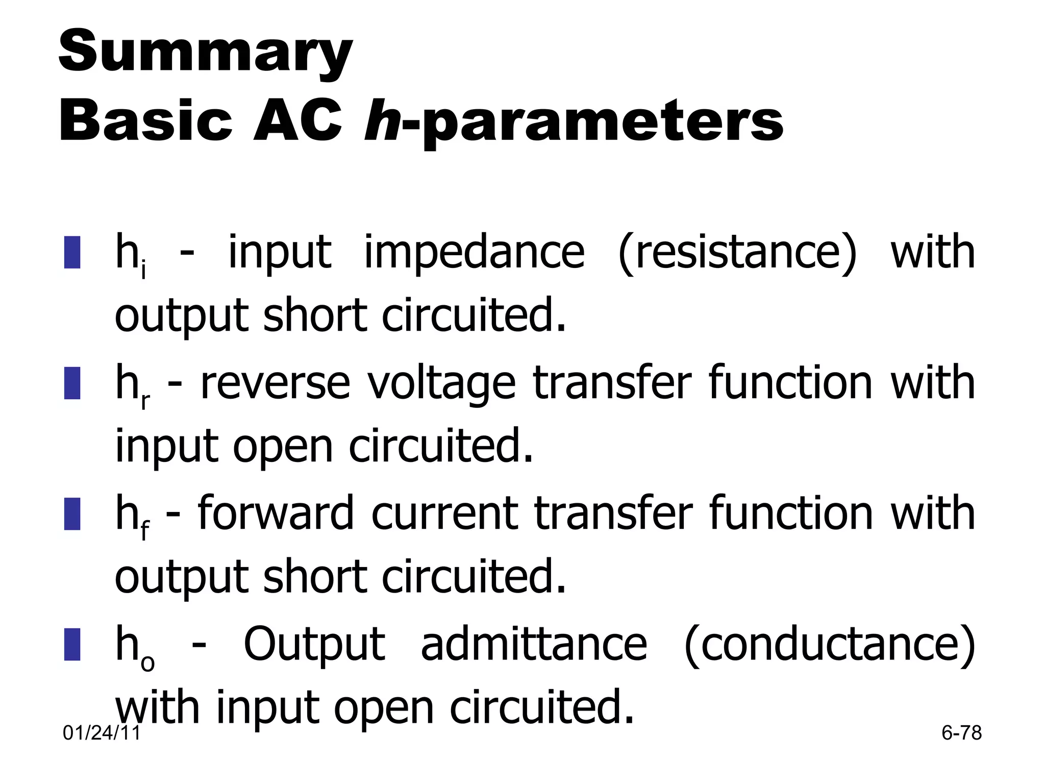
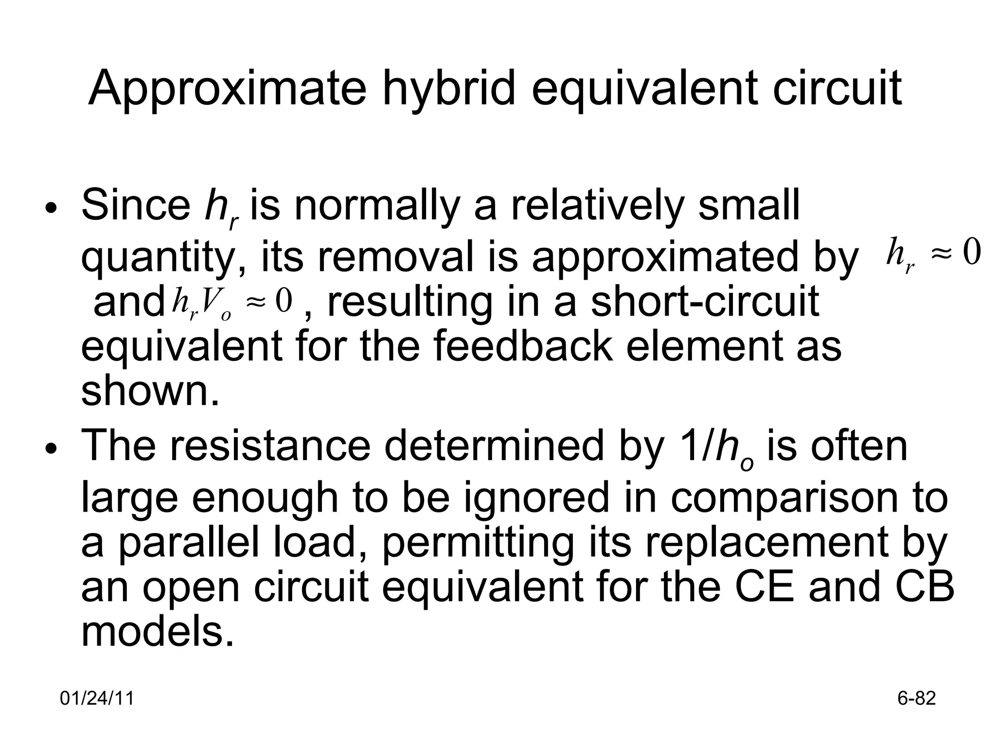
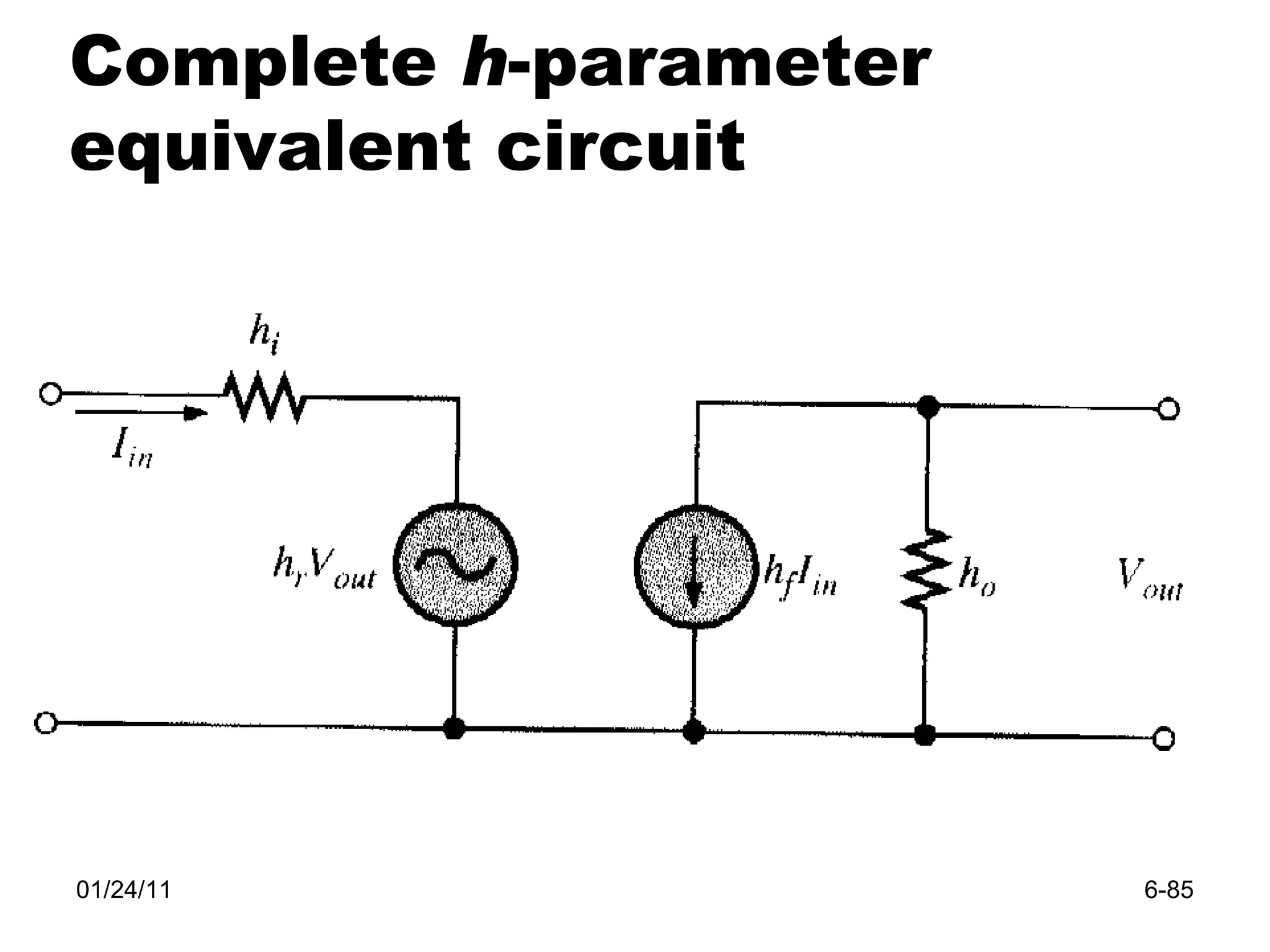
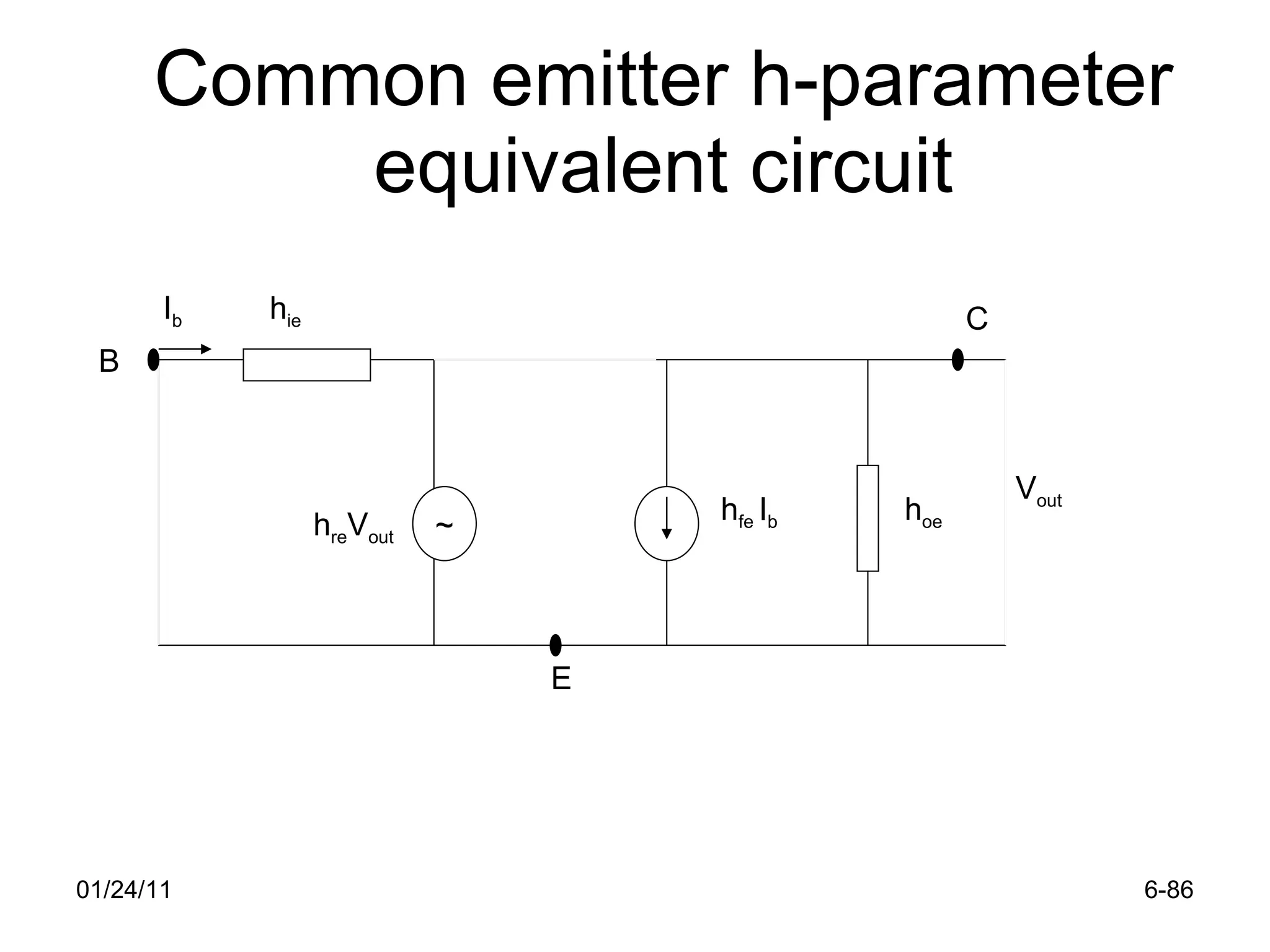
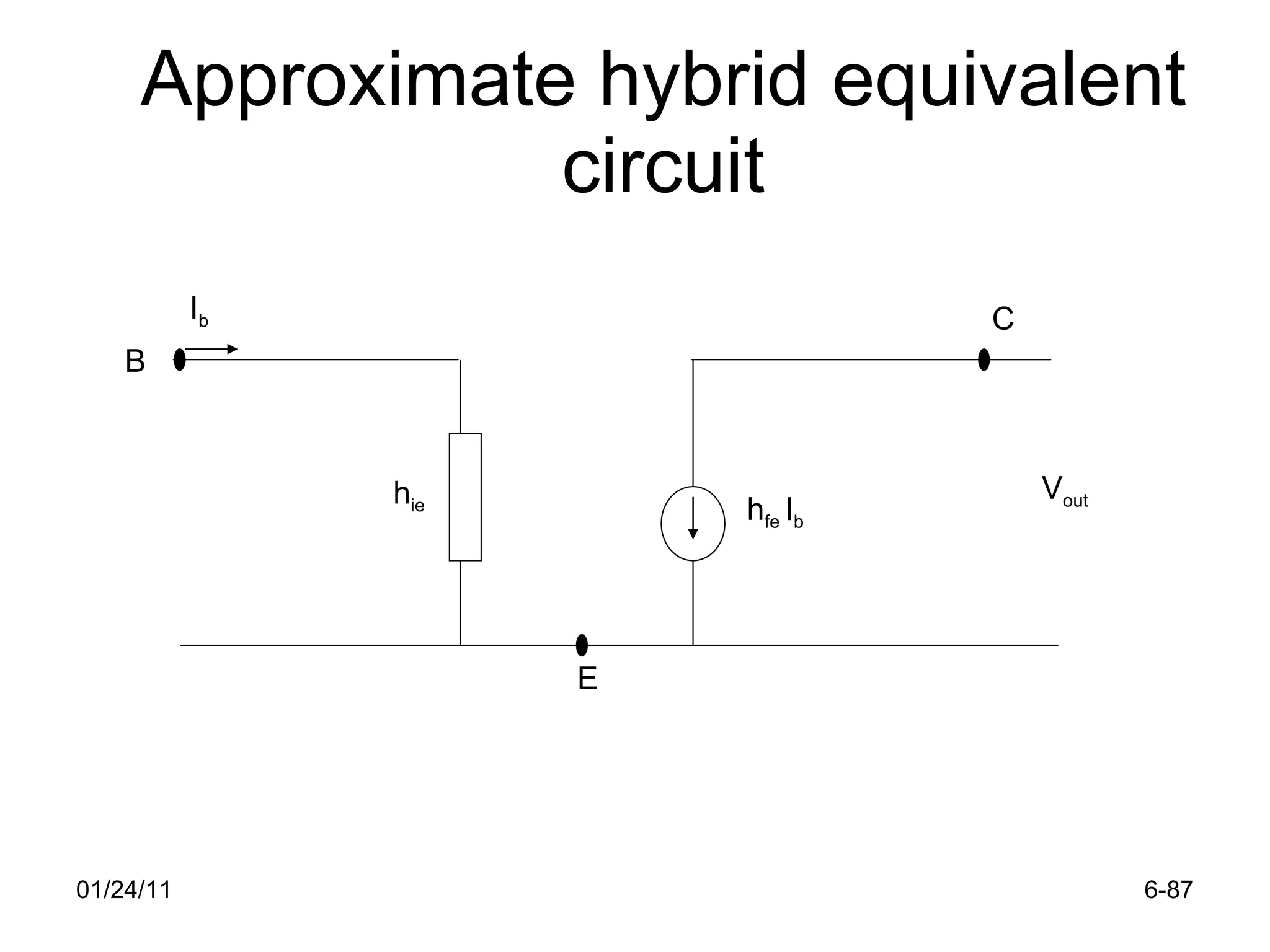
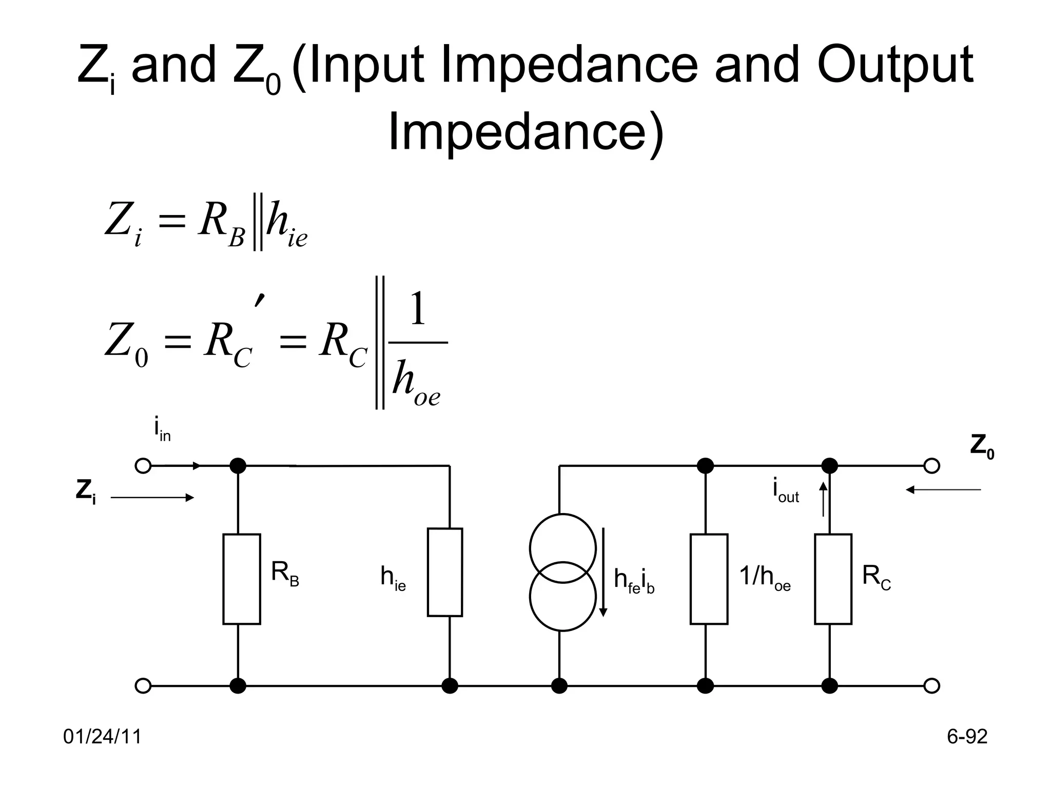
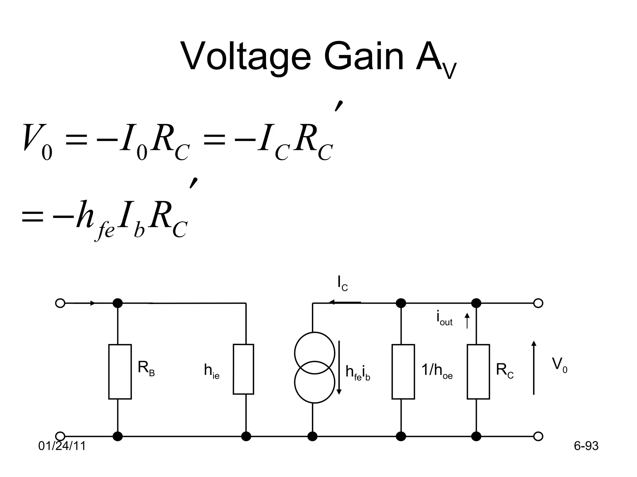
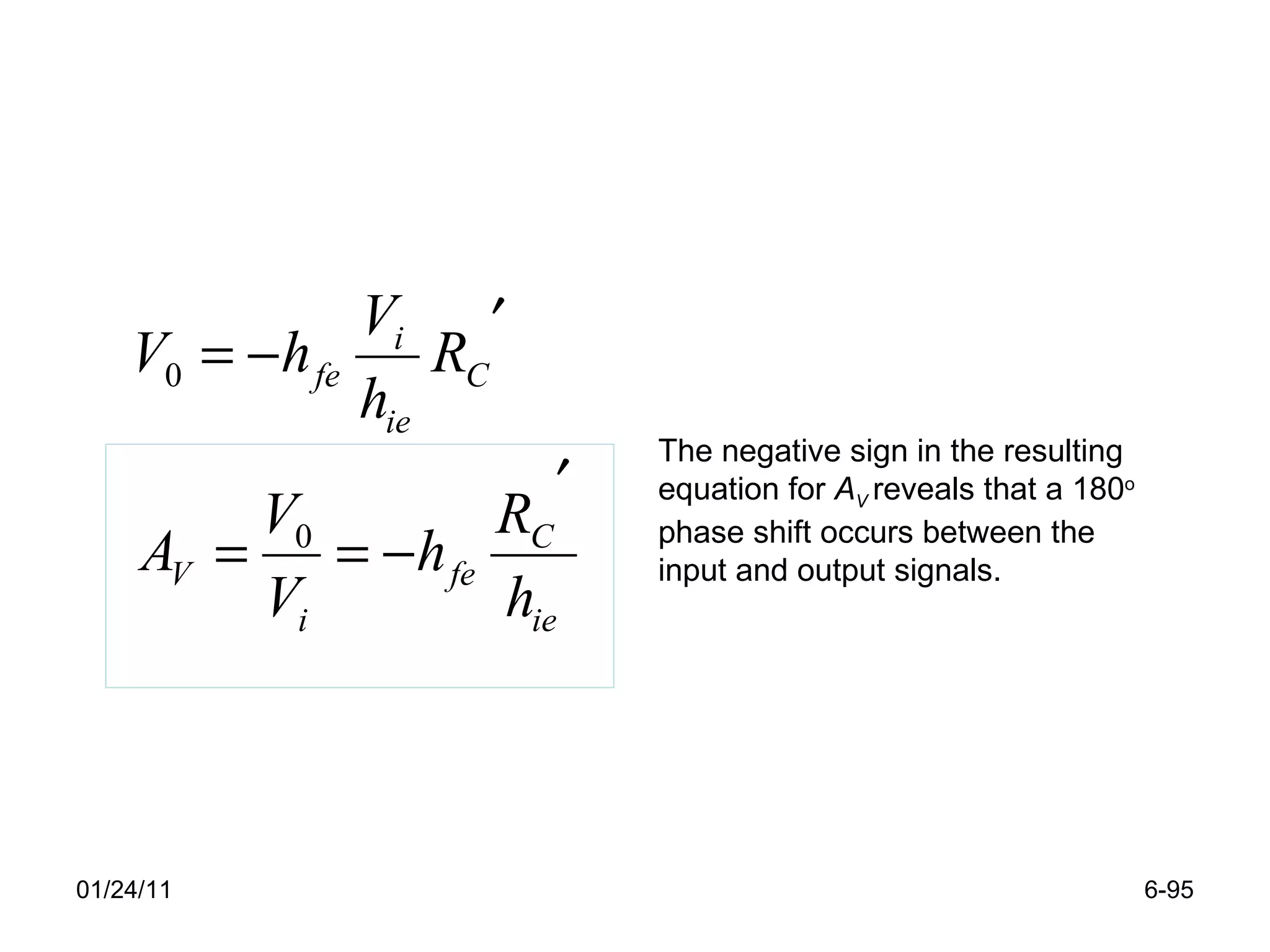
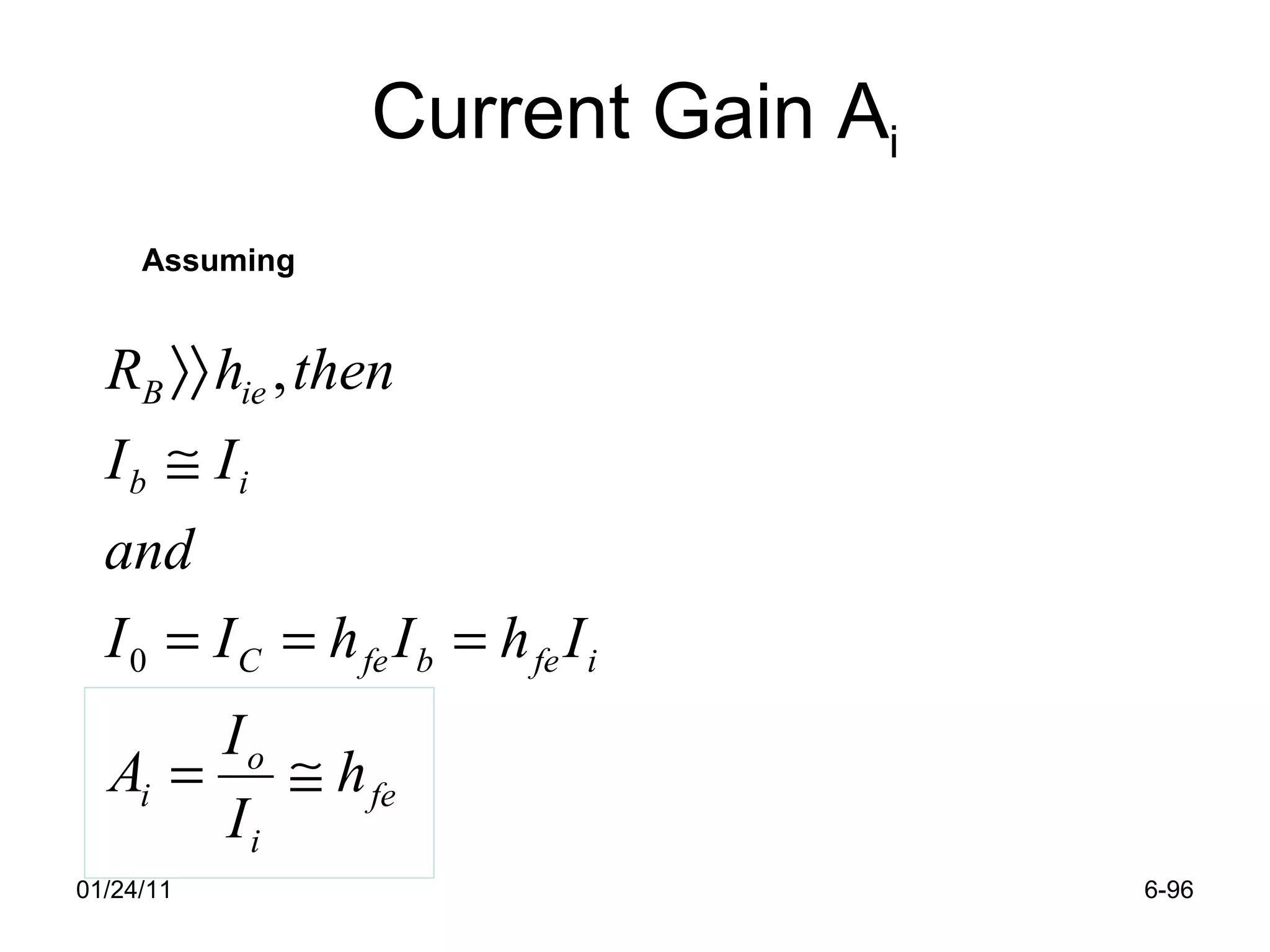
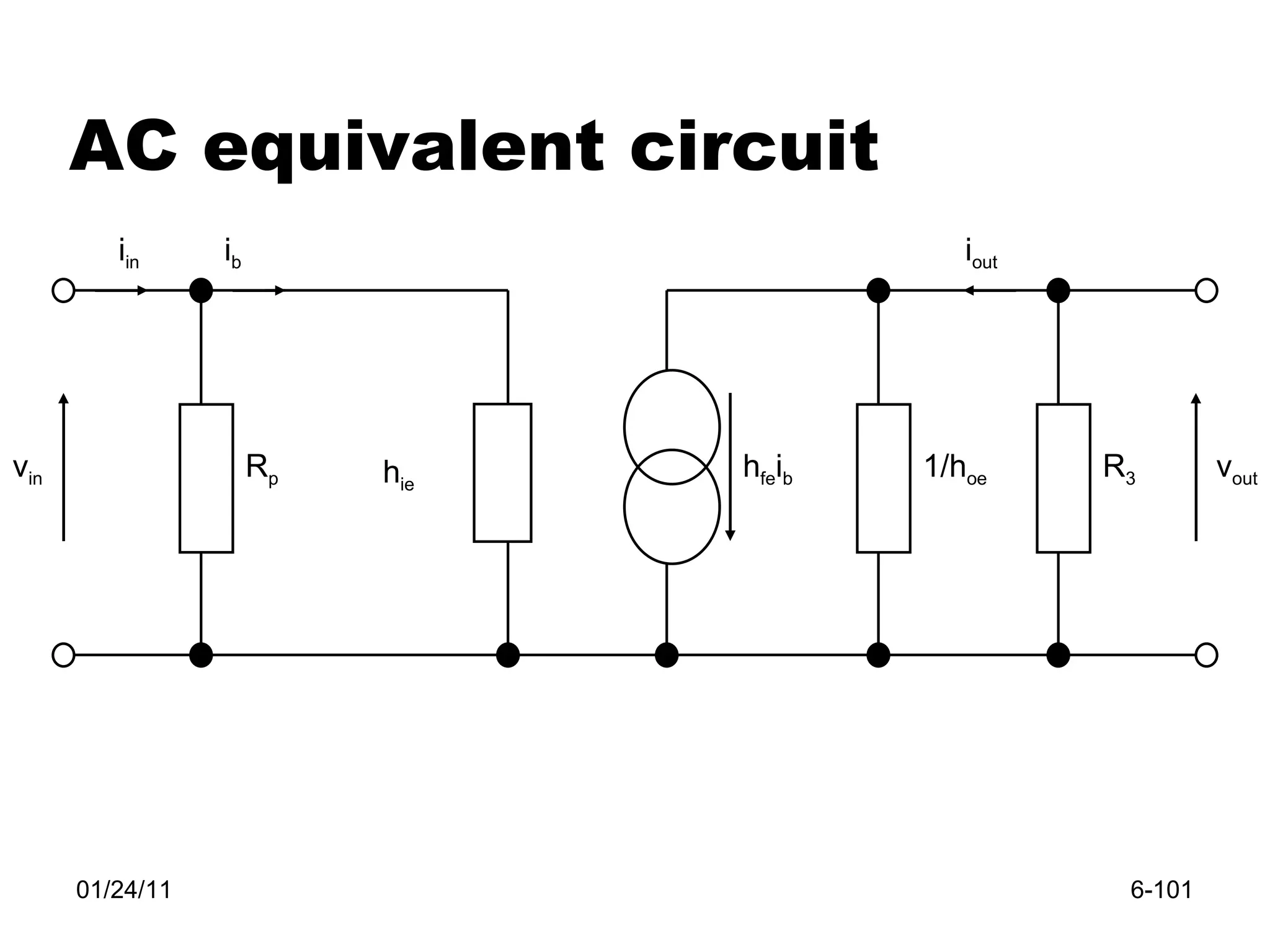
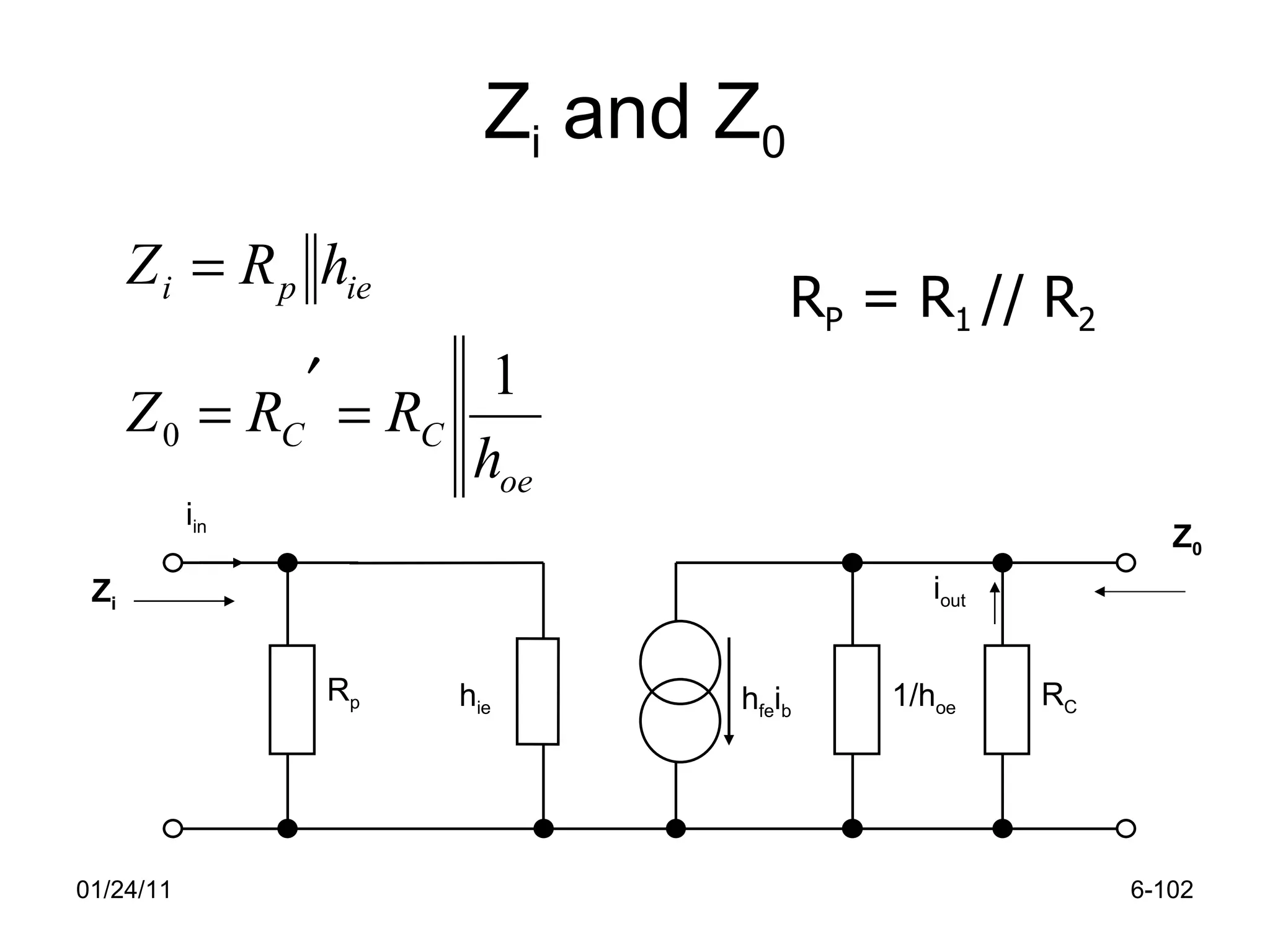
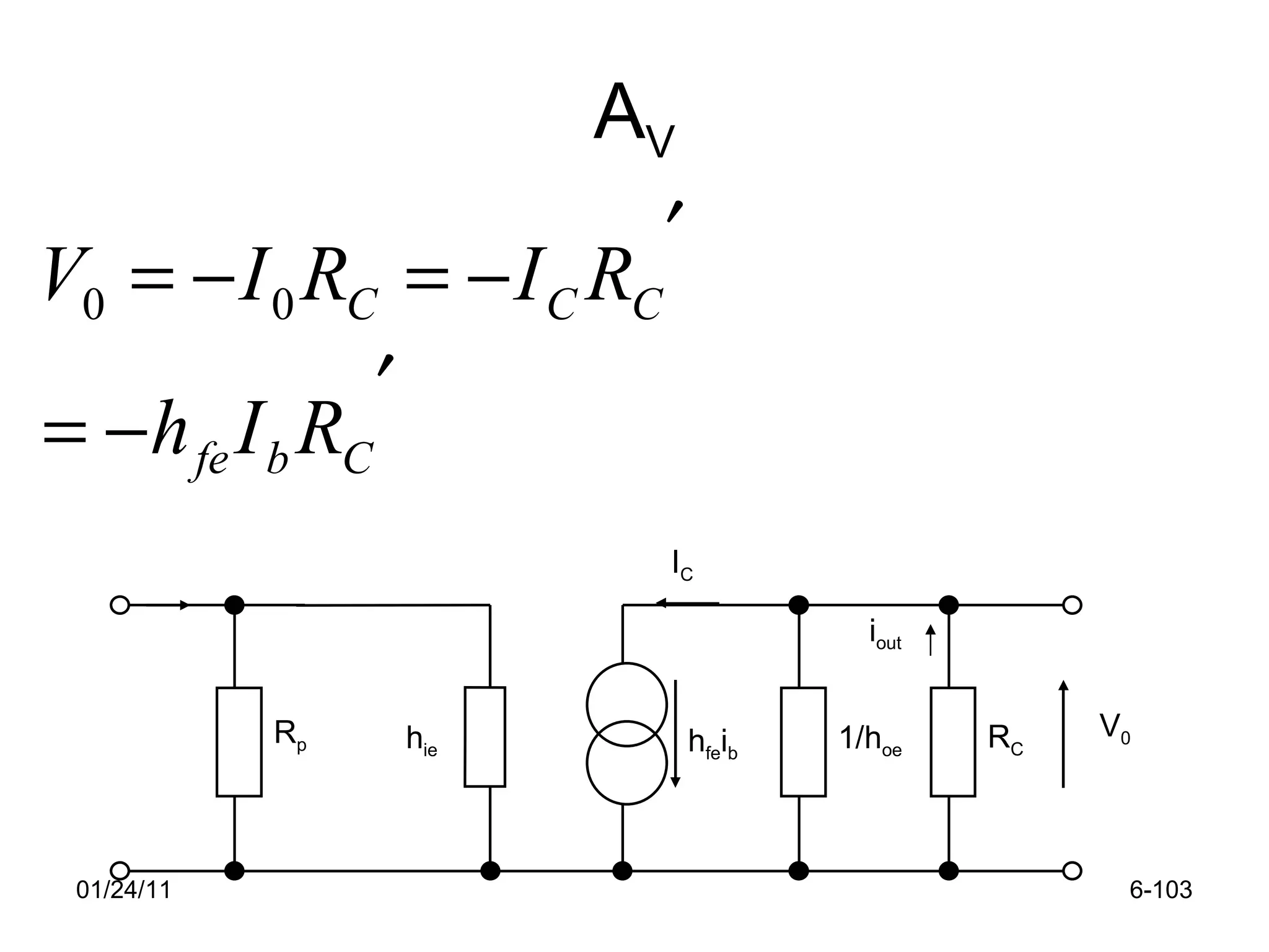
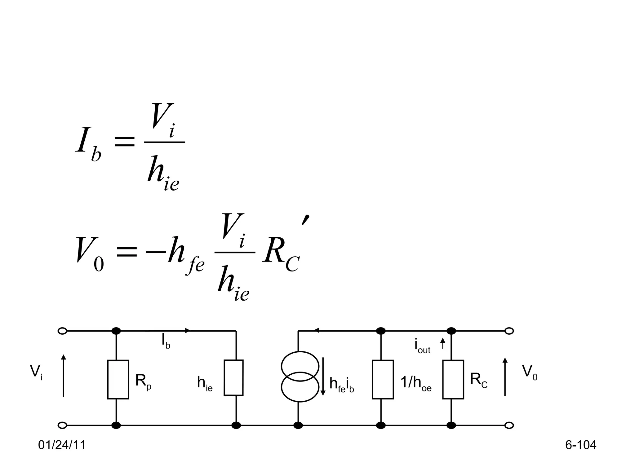
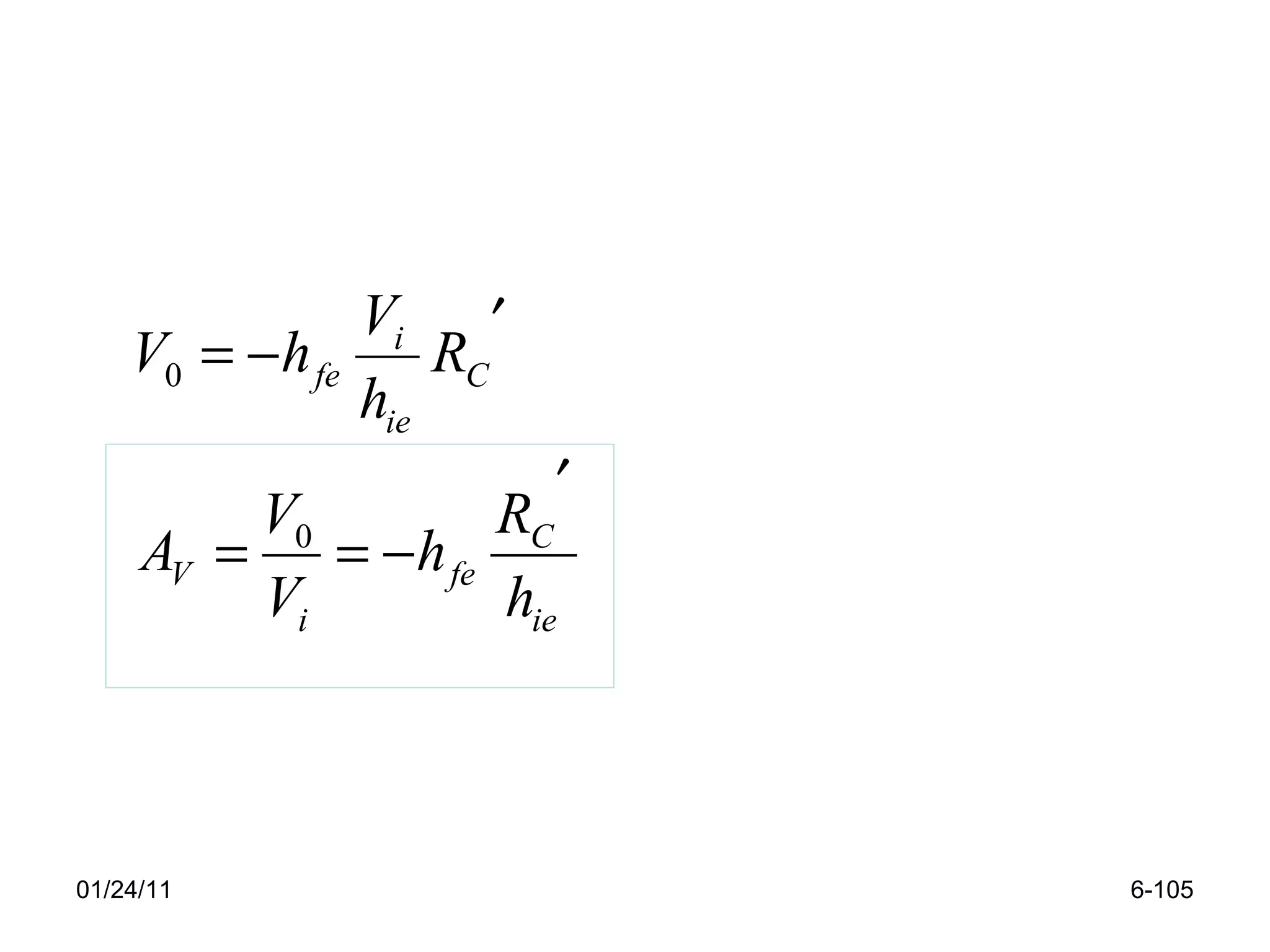
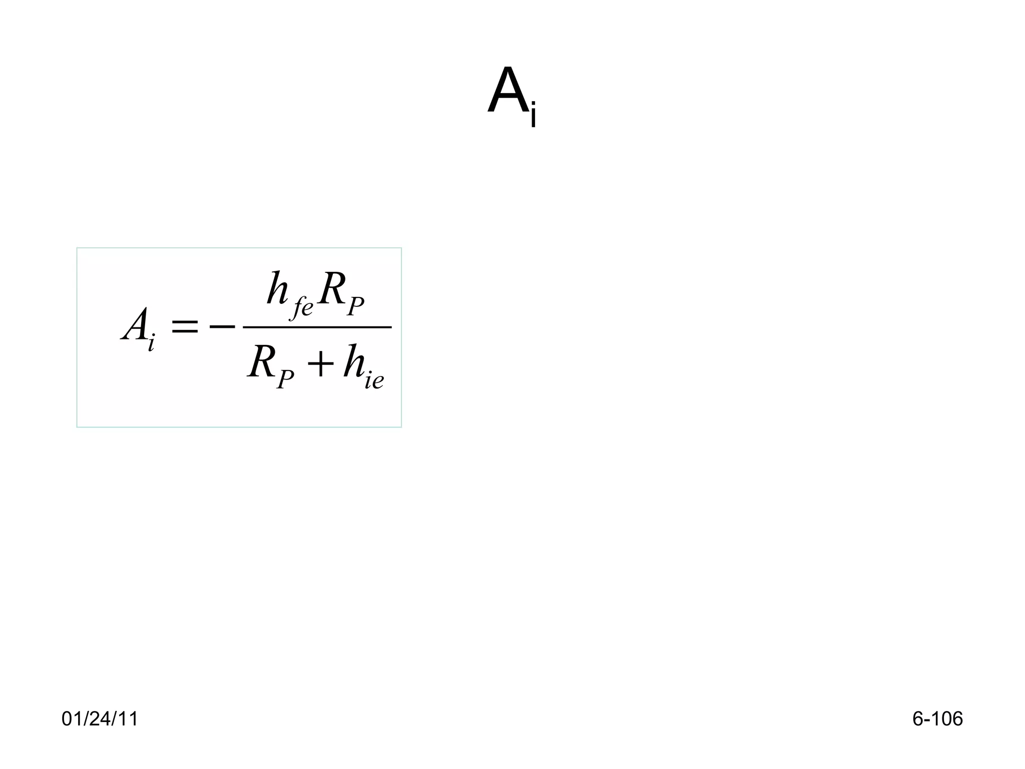
- Hybrid-pi and h-parameter transistor models for AC analysis.
So in summary, it discusses rectifier circuits, transistor biasing methods, amplifier configurations, key transistor parameters, and transistor modeling for analysis of small-